EP1093017A2 - Méthode et dispositif d'inspection de réticules utilisant l'imagerie aérienne - Google Patents
Méthode et dispositif d'inspection de réticules utilisant l'imagerie aérienne Download PDFInfo
- Publication number
- EP1093017A2 EP1093017A2 EP00122146A EP00122146A EP1093017A2 EP 1093017 A2 EP1093017 A2 EP 1093017A2 EP 00122146 A EP00122146 A EP 00122146A EP 00122146 A EP00122146 A EP 00122146A EP 1093017 A2 EP1093017 A2 EP 1093017A2
- Authority
- EP
- European Patent Office
- Prior art keywords
- reticle
- aerial images
- die
- image
- images
- Prior art date
- Legal status (The legal status is an assumption and is not a legal conclusion. Google has not performed a legal analysis and makes no representation as to the accuracy of the status listed.)
- Granted
Links
Images


Classifications
-
- G—PHYSICS
- G03—PHOTOGRAPHY; CINEMATOGRAPHY; ANALOGOUS TECHNIQUES USING WAVES OTHER THAN OPTICAL WAVES; ELECTROGRAPHY; HOLOGRAPHY
- G03F—PHOTOMECHANICAL PRODUCTION OF TEXTURED OR PATTERNED SURFACES, e.g. FOR PRINTING, FOR PROCESSING OF SEMICONDUCTOR DEVICES; MATERIALS THEREFOR; ORIGINALS THEREFOR; APPARATUS SPECIALLY ADAPTED THEREFOR
- G03F7/00—Photomechanical, e.g. photolithographic, production of textured or patterned surfaces, e.g. printing surfaces; Materials therefor, e.g. comprising photoresists; Apparatus specially adapted therefor
- G03F7/70—Microphotolithographic exposure; Apparatus therefor
- G03F7/70058—Mask illumination systems
- G03F7/70091—Illumination settings, i.e. intensity distribution in the pupil plane or angular distribution in the field plane; On-axis or off-axis settings, e.g. annular, dipole or quadrupole settings; Partial coherence control, i.e. sigma or numerical aperture [NA]
- G03F7/701—Off-axis setting using an aperture
-
- G—PHYSICS
- G03—PHOTOGRAPHY; CINEMATOGRAPHY; ANALOGOUS TECHNIQUES USING WAVES OTHER THAN OPTICAL WAVES; ELECTROGRAPHY; HOLOGRAPHY
- G03F—PHOTOMECHANICAL PRODUCTION OF TEXTURED OR PATTERNED SURFACES, e.g. FOR PRINTING, FOR PROCESSING OF SEMICONDUCTOR DEVICES; MATERIALS THEREFOR; ORIGINALS THEREFOR; APPARATUS SPECIALLY ADAPTED THEREFOR
- G03F1/00—Originals for photomechanical production of textured or patterned surfaces, e.g., masks, photo-masks, reticles; Mask blanks or pellicles therefor; Containers specially adapted therefor; Preparation thereof
- G03F1/68—Preparation processes not covered by groups G03F1/20 - G03F1/50
- G03F1/82—Auxiliary processes, e.g. cleaning or inspecting
- G03F1/84—Inspecting
-
- G—PHYSICS
- G03—PHOTOGRAPHY; CINEMATOGRAPHY; ANALOGOUS TECHNIQUES USING WAVES OTHER THAN OPTICAL WAVES; ELECTROGRAPHY; HOLOGRAPHY
- G03F—PHOTOMECHANICAL PRODUCTION OF TEXTURED OR PATTERNED SURFACES, e.g. FOR PRINTING, FOR PROCESSING OF SEMICONDUCTOR DEVICES; MATERIALS THEREFOR; ORIGINALS THEREFOR; APPARATUS SPECIALLY ADAPTED THEREFOR
- G03F7/00—Photomechanical, e.g. photolithographic, production of textured or patterned surfaces, e.g. printing surfaces; Materials therefor, e.g. comprising photoresists; Apparatus specially adapted therefor
- G03F7/70—Microphotolithographic exposure; Apparatus therefor
- G03F7/70058—Mask illumination systems
- G03F7/70125—Use of illumination settings tailored to particular mask patterns
-
- G—PHYSICS
- G03—PHOTOGRAPHY; CINEMATOGRAPHY; ANALOGOUS TECHNIQUES USING WAVES OTHER THAN OPTICAL WAVES; ELECTROGRAPHY; HOLOGRAPHY
- G03F—PHOTOMECHANICAL PRODUCTION OF TEXTURED OR PATTERNED SURFACES, e.g. FOR PRINTING, FOR PROCESSING OF SEMICONDUCTOR DEVICES; MATERIALS THEREFOR; ORIGINALS THEREFOR; APPARATUS SPECIALLY ADAPTED THEREFOR
- G03F7/00—Photomechanical, e.g. photolithographic, production of textured or patterned surfaces, e.g. printing surfaces; Materials therefor, e.g. comprising photoresists; Apparatus specially adapted therefor
- G03F7/70—Microphotolithographic exposure; Apparatus therefor
- G03F7/70483—Information management; Active and passive control; Testing; Wafer monitoring, e.g. pattern monitoring
- G03F7/70605—Workpiece metrology
- G03F7/70616—Monitoring the printed patterns
-
- G—PHYSICS
- G03—PHOTOGRAPHY; CINEMATOGRAPHY; ANALOGOUS TECHNIQUES USING WAVES OTHER THAN OPTICAL WAVES; ELECTROGRAPHY; HOLOGRAPHY
- G03F—PHOTOMECHANICAL PRODUCTION OF TEXTURED OR PATTERNED SURFACES, e.g. FOR PRINTING, FOR PROCESSING OF SEMICONDUCTOR DEVICES; MATERIALS THEREFOR; ORIGINALS THEREFOR; APPARATUS SPECIALLY ADAPTED THEREFOR
- G03F7/00—Photomechanical, e.g. photolithographic, production of textured or patterned surfaces, e.g. printing surfaces; Materials therefor, e.g. comprising photoresists; Apparatus specially adapted therefor
- G03F7/70—Microphotolithographic exposure; Apparatus therefor
- G03F7/70483—Information management; Active and passive control; Testing; Wafer monitoring, e.g. pattern monitoring
- G03F7/70605—Workpiece metrology
- G03F7/70616—Monitoring the printed patterns
- G03F7/70633—Overlay, i.e. relative alignment between patterns printed by separate exposures in different layers, or in the same layer in multiple exposures or stitching
Definitions
- This invention relates to techniques for inspecting reticles that are used in fabricating microelectronic devices through a microphotolithographic process.
- the present invention relates to a method and an apparatus for detecting variations in line width and other defects that would be printed on the wafer using such reticles by emulating the operation of a specific photolithography tool in which this reticle is to be used.
- the invention is embodied in a method and an apparatus that can readily be used for inspecting reticles in the industrial environment.
- Modern microelectronic devices are commonly produced using a photolithographic process.
- a semiconductor wafer is first coated with a layer of photoresist.
- This photoresist layer is then exposed to illuminating light using a photomask (for simplicity, the terms photomask, mask, and reticle will be used here interchangeably) and subsequently developed.
- a photomask for simplicity, the terms photomask, mask, and reticle will be used here interchangeably
- the exposed photoresist produces the image of the mask on the wafer.
- the uppermost layer of the wafer is etched.
- the remaining photoresist is stripped.
- the above procedure is then repeated to produce subsequent patterned layers.
- RET Resolution Enhancement Techniques
- OPC Optical Proximity Correction
- PSM Phase Shift Mask
- the layout of the design of the mask is altered in such a way that the mask produces a higher resolution image on the photoresist.
- the optical proximity corrections introduced into the mask design compensate for the optical proximity effects caused by the limited resolution of the optical exposure system used in the photolithographic process.
- An optical stepper is one example of the optical exposure system.
- Other types of optical exposure systems include optical scanners and step-and-scan exposure systems.
- Most common optical proximity effects include corner rounding, line end shortening, and line width non-linearity.
- Processing of the mask including mask etching also contributes to the proximity effects.
- To correct for the proximity effects such as corner rounding, reentrant and outside serifs are added to the mask design, and to correct for the line width variations, so called sub-resolution features are used.
- a mask must be as defect-free as possible, preferably completely defect-free. Therefore, mask inspection tools are needed to detect various defects in the masks that can potentially reduce the microelectronic circuit fabrication yields.
- Certain kinds of mask defects can be detected by inspecting the mask using the image of the mask produced by the light transmitted through the mask and the light reflected by one face of the mask.
- the mask inspection tool that uses this method acquires both images and analyzes them. The results of the analysis of the two images yield the information on the condition of the mask.
- the image analysis may use die-to-die comparison, die-to-database comparison, or reflected image to transmitted image comparison.
- the die-to-die comparison method the acquired images of a die of the mask are compared to the images of another die from the same mask.
- the die-to-database method the acquired images are compared to images that are simulated using the design specifications.
- Such an inspection system can detect defects that may or may not print on the photoresist during the actual photolithographic process.
- the major drawback of this method is that it studies the physical structure of the mask independently of the optical image actually produced by the mask on the wafer. For instance, variations in the line width of the image that the mask produces frequently are higher than the corresponding variation in the line width of the mask itself . This phenomenon is called MEEF (Mask Error Enhancement Factor).
- MEEF Mesk Error Enhancement Factor
- PSM in which there is no visible relation between phase error and the printed image. It is desirable, therefore, to relate the physical structure of the mask to the actual image that the mask creates on the photoresist, and to study directly the image that the mask actually produces.
- AIMSTM Aerial Image Measurement System
- the Zeiss MSM100 a mask development tool, implementing AIMSTM technology, is available commercially from Carl Zeiss, GmbH of Germany.
- the MSM100 system can be used to evaluate the printability properties of newly developed masks.
- the inspection system simulates an optical exposure system that is used to expose the photoresist during semiconductor device fabrication.
- the optical system of the mask inspection device uses a set of the exposure conditions, that are used in the actual microphotolithographic process to create an image that would be produced on the photoresist during actual device fabrication.
- the system matches the wavelength, the partial coherence of the exposure light, illumination aperture and the imaging numerical aperture NA of the optical exposure system.
- the created aerial image is magnified and detected using a CCD camera that is sensitive to ultraviolet radiation.
- the use of the aerial imaging method permits the detection of the mask defects that would print during the actual microphotolithographic process.
- Almost any kind of defect on the reticle including a particle on the transparent region, a pin-hole, a pin-dot, an edge truncation, etc. causes line width variation in the printed image.
- the term "line width” used herein describes a set of parameters of the image produced by the reticle on the photoresist, such as wire-to-wire distances, that determine whether the reticle is to be rejected as defective.
- the acquired aerial images are analyzed using the AIMSTM software also developed by IBM.
- U.S. Patent No. 5,481,624 describes a system that uses aerial imaging for die-to-database inspection of phase shift masks. According to the described inspection method, an aerial image produced by a phase-shift mask is verified against the original circuit pattern that was used in manufacturing of the mask.
- U.S. Patent No. 5,795,688 discloses a system that uses an aerial imaging method for inspection of microphotolithographic masks having optical proximity corrections using a die-to-database comparison.
- an aerial image of a mask manufactured using the aforementioned optical proximity corrections is compared to an aerial image of the same mask obtained by simulation.
- Various defects in the mask such as missing chrome, contamination, glass damage, phase defects, and transmission errors are identified as discrepancies between the two images.
- the simulation process takes into account optical proximity effects due to the limited resolution of the optical exposure system and the proximity effects due to the photoresist etching during the mask manufacturing process.
- the simulated aerial image can be obtained using the original mask design or, alternatively, using the mask design corrected for optical proximity effects.
- the IBM system is designed for mask development labs, and not for production stage mask inspection, and therefore does not possess adequate automation.
- the inspection methods based on die-to-database comparison that are used by the existing aerial imaging systems are not always effective, especially for highly complicated mask designs.
- the die-to-database comparison method uses models describing the behavior of an optical exposure system, as well as the effects of the etching used in the mask manufacturing process to produce the simulated image used in the mask inspection.
- the actual mask is different from the mask design due to limitations of the mask writing tool.
- the limitations on the quality of the simulated images limit the performance of the aerial imaging inspection techniques that use the die-to-database comparison.
- the system also must be capable of detecting the presence of surface defects such as particles, contaminations, coating defects, and the like.
- the mask inspection system It also isdesirable for the mask inspection system to provide speedy and reliable identification of the above mask defects. Such a system would be able to work efficiently in a clean manufacturing environment such as fabs and mask shops and increase the productivity thereof.
- the present invention intends to overcome the above problems.
- the object is solved by the method and apparatus for inspecting according to independent claim 1.
- a method for inspecting a multiple die reticle that is used with an optical exposure system under a set of exposure conditions, the multiple die reticle including at least a first and a second die.
- a plurality of images of the reticle are acquired using transmitted light under the indicated exposure conditions.
- the plurality of images of the reticle includes images of the first die and images of the second die.
- Each of the plurality of images of the reticle corresponds to a different focal condition.
- the images of the first die and the second die are used to detect variations in line width in the first die.
- an apparatus which can be used to practice the inventive method.
- the apparatus includes a scanner for acquiring a plurality of images of the multiple die reticle under the set of exposure conditions.
- the plurality of images includes images of the first die and images of the second die.
- the apparatus also includes an image processing module for detecting variations in line width of the first die by comparing the images of the first die and the images of the second die.
- an apparatus including: a laser light source; a homogenizer and a transmission light illumination means for illuminating the reticle; and an optical system for producing a plurality of magnified images of the reticle under the set of exposure conditions, the optical system having variable illuminating and imaging apertures for reproducing the indicated set of exposure conditions.
- the plurality of acquired images of the reticle includes images of the first die and images of the second die.
- the inventive apparatus also includes an image acquisition module for acquiring the plurality of magnified images of the reticle; and an image processing module for analyzing a condition of the reticle by comparing the images of the first die and the images of the second die.
- the apparatus also includes an optical system for acquiring dark field reflection images.
- a reticle inspection system for inspecting reticles which can be used as an incoming inspection tool, and as a periodic and pre-exposure inspection tool.
- Mask shops can use it as an inspection tool compatible to their customers, and as a printable error detection tool.
- the inventive system detects two kinds of defects: (1) line width errors in the printed image; (2) surface defects.
- the line width errors are detected on the die area.
- the detection is performed by acquiring the image of the reticle under the same optical conditions as the exposure conditions, (i.e. wavelength, numerical aperture, sigma, and illumination aperture type) and by comparing multiple dies to find errors in the line width.
- Surface defects are detected all over the reticle.
- the detection of surface defects is performed by acquiring transmission and dark-field reflection images of the reticle and using the combined information to detect particles, and other surface defects.
- the system for defect detection is composed of three main modules: (1) a scanner module; (2) a defect detection image processing hardware module; and (3) a post process and review station.
- the scanner module scans the reticle and acquires aerial images of the reticle in transmitted light at a plurality of focal planes, preferably three, and dark field images of the reticle in reflected light at one focal plane.
- the NA and the coherence factor are adjusted.
- the optical system of the scanner module simulates the behavior of an optical exposure system and, as a result, the acquired transmission light aerial images are optically equivalent to those produced on the photoresist under a given set of exposure conditions.
- the image processing module then uses the acquired images to detect the defects in the reticle.
- the system detects reticle defects, such as line width errors, by using die-to-die comparison of the aerial images of multiple dies.
- "surface" defects in the reticle are detected by comparing the transmission images of the reticle to the dark field reflection images of the reticle.
- the reflection to transmission image comparison procedure operates on the entire scanned area of the reticle regardless of the dies.
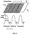
- the scanning of the reflection images is separated in time from scanning of the transmission images. Such separation can be accomplished by using a separate scan for each particular type of image. For instance, during the first scan the system acquires the reflection image, and during the second scan the system acquires the transmission image.
- the time separation may also be achieved by acquiring both types of images in an interlace mode, as shown in Fig. 4. In Fig.
- a table holding the reticle is moved in such a way, that the camera frame 201 moves continuously relative to the surface of the reticle.
- Light pulses 202 and 203 are generated alternatingly using the transmission and the reflection light illumination systems, respectively. Therefore, the camera acquires images of the reticle alternatingly in transmitted and reflected light.
- the camera window is arranged is such a way, that the camera simultaneously acquires images of two rectangular spots of the reticle, which provides for continuity of image acquisition.
- the imaging resolution need not be the same for the two detection modes.
- a software-based post process and review station reviews and analyzes the images of the detected defects through the focus range of the exposure system.
- the scanner unit scans the entire active area of the reticle and acquires sequentially three or four digital images: two or three transmission aerial images at different focal planes, and a dark field reflection image.
- the scanner unit supplies the scanned images of the detected defects acquired during scanning for off-line review.
- the scanner unit is also capable of acquiring additional aerial images of the detected defects at additional focal planes during the review stage.
- Fig. 1 illustrates the internal organization of the scanner unit.
- the scanner unit includes many of the components of an optical microscope column. With reference to Fig. 1, the scanner scans a reticle 1 fixed on a moving stage 2. Laser light from a light source 3 is used to illuminate the reticle 1.
- the light source 3 preferably is a pulsed laser source, but the light source 3 could also operate continuously.
- the radiation provided by the light source 3 preferably has the exact wavelength of the exposure system, with which the reticle is designed to be exposed, for example deep UV (248nm) or 193nm.
- the scanner module When the scanner module acquires the aerial images of the reticle in the transmitted light, the bottom surface of the reticle is illuminated using a transmission light illumination system which includes a homogenizer and illumination optics 5, an illumination aperture 7, and a condenser 6,
- the homogenizer has a function, among others, of reducing speckle resulting from the use of a coherent illumination source.
- the structure of the homogenizer is not critical, so long as the homogenizer reduces speckle appropriately.
- the aerial images of the reticle 1 acquired by the scanner module simulate the images that would be produced by the reticle 1 on the photoresist, when the reticle 1 is placed on an optical exposure system.
- the radiation from the illuminating light source 3 passes through the homogenizer and illumination optics 5 and the condenser 6.
- the condenser 6 reduces the diameter of the illuminating beam of light in the reticle plane to just a little more than the size of the field of view of the imaging system.
- an illumination numerical aperture 7 NA ill
- Adjusting the size and the shape of the illumination aperture 7 permits reproduction of the illumination and the coherence conditions of the photoresist exposure tool.
- the aperture 7 is selected to set the proper coherence ratio sigma and to choose between on axis and off axis illumination such as a quadrupole or an annular mode of illumination, as described below.
- the objective 10 collects the light transmitted by the reticle 1 in the transmission light illumination operating mode and the light reflected by the reticle in the dark field illumination operating mode. After passing through the objective 10, the light passes through the collecting adjustable numerical aperture diaphragm 12, which is situated in the optically designed aperture stop surface or a conjugate surface.
- the size of the collecting numerical aperture diaphragm 12 is selected to reproduce the operating conditions of the exposure system used in the microphotolithographic process. Therefore, the aerial image of the reticle 1 created by the optical system of the reticle inspection apparatus according to the invention is equivalent to the image produced on the photoresist by the optical exposure system during the microphotolithographic process.
- the light emerging from the numerical aperture 12 is then focused by a lens, such as tube lens 13 to produce an image of the reticle 1, This image is then magnified by a zoom magnification lens 14.
- the light beam is being split by a beam splitter 15 to produce three images of the reticle in the three CCD cameras of the reticle inspection apparatus: a first focus/dark field reflection camera 16, a second focus camera 17, and a third focus camera 18.
- a first focus/dark field reflection camera 16 a second focus camera 17, and a third focus camera 18.
- the dark field illumination system 4 directs a beam of illuminating light from the laser source 3 at the top face of the reticle 1.
- the light from laser source 3 directed at the top face of the reticle 1 by the dark field illumination system passes through a annular numerical aperture (NA ann ) diaphragm 12'.
- NA ann numerical aperture
- the aperture 12' is ring-shaped so that the light, after passing through the aperture 12', goes around objective 10 and illuminates reticle 1.
- the illuminating light emerging from the dark field illumination system 4 passes through the objective 10 and again illuminates reticle 1.
- this illuminating light is reflected by the reticle 1 and travels in the opposite direction, passing through the objective 10 and then through the collecting numerical aperture (NA coll ) diaphragm 12, before being detected as described above.
- the dark field illumination system 4 is placed to the side of the objective 10 so as to illuminate the top face of the reticle 1 from the side. In this configuration, the illuminating light from the dark field illumination system 4 need not pass through the NA diaphragm 12 and objective 10.
- the system is equipped with a suitable auto-focusing system (not specifically shown) aimed at maintaining the inspection plane of the reticle in the focal plane of the objective 10. This is generally done by providing motion of the stage 2 or the objective 10 in the Z direction.
- the reticle inspection apparatus When the reticle inspection apparatus according to the invention operates in the dark field illumination mode, the top face of the reticle 1 is illuminated by the dark field illumination system 4 and the first focus/dark field reflection camera 16 acquires the image of the reticle 1 in the reflected light.
- the reticle inspection apparatus when the reticle inspection apparatus operates in the transmission light illumination mode, the reticle 1 is illuminated by the transmission light illumination system 5 and the three images of the reticle in the transmitted light are simultaneously acquired by the first focus/dark field reflection camera 16, the second focus camera 17, and the third focus camera 18.
- the first focus camera 16 is in focus
- the second and the third focus cameras 17 and 18 are at the edges of the simulated process window of the exposure system.
- process window refers to the acceptable range of the focus and the exposure dose that can be used in the exposure of the reticle by the exposure system to achieve the image on the photoresist, which satisfies the requirements of the wafer specification.
- the second focus camera 17 is at one edge of the process window, while the third focus camera 18 is at the other edge.
- the aerial images of the reticle created in the cameras 16-18 are significantly magnified (typically x50-x200).
- the image of the reticle is demagnified (typically x1/4-x1/5).
- the process window for creating the aerial image is so magnified, as to allow a large variation in the positions of the focal planes of the cameras.
- the positions of these focal planes can be adjusted by conventional mechanical means.
- the images of the reticle acquired by cameras 16-18 can be used to determine the process window of the reticle exposure system. This can be done through comparison of the aerial images of the reticle, acquired under different exposure and focal conditions, with the corresponding design specifications of the wafer.
- the focal position of the system can be further finely adjusted by displacing the reticle in z-direction, as shown in figure 1.
- the method of operation of the inventive reticle inspection apparatus is described below.
- the stage 2 moves the reticle 1, in such a way that the scanner unit scans the reticle, slice-by-slice in a serpentine manner.
- the width of a slice is preferably the width of the optical field of view of the system.
- the CCD cameras 16, 17, and 18 can be line CCD devices capable of simultaneously acquiring an image of the entire slice of the reticle 1.
- CCD cameras 16, 17, and 18 can be of a shift-delay type.
- the cameras 16-18 are sensitive in the ultraviolet range, particularly in the deep UV range.
- the moving stage 2 and the reticle 1 move in a continuous manner.
- the CCD cameras 16, 17, and 18 are triggered by the stage 2 to acquire the image of the slice of the reticle 1 every time the stage has passed one field of view.
- the image of the reticle is acquired by shooting a laser pulse from laser source 3 through the illumination optics 4 or 5 of the system and acquiring the images with digital area cameras 16-18 through the imaging optics. It will be appreciated that if the pulsed laser source is used to illuminate the reticle, the reticle need not be stationary at the time of the image capture and, for this reason, the reticle can be moved continuously. The same result can be achieved through using a short exposure time for the cameras 16-18.
- the stage 2 and the reticle 1 move in a stepwise manner.
- the optics of the scanner unit emulates the optics of an exposure tool.
- the illumination aperture 7 selectively alters the effective illuminating NA ill of the condenser 6, while the aperture 12 changes the collection numerical aperture NA coll of the objective 10.
- a ratio of the NA ill to the NA coll is called a pupil filling ratio of the objective and is responsible for the coherence of the reticle illumination. The smaller the value of the pupil filling ratio, the higher the coherence of the reticle illumination.
- the numerical aperture 7 can have more complex configuration, for example four small apertures displaced with respect to the axis of the beam. Other illumination aperture configurations can be used to emulate different exposure systems and their interaction with the reticle.
- the illumination numerical aperture 7 can be used to shape the light beam to more closely resemble the exposure tool.
- the illumination aperture 7 may be a diffractive optical element or a proper apodization aperture affecting also the shape of the incident beam.
- the aperture 7 can provide a flat-top beam, i.e. a beam with uniform intensity distribution over the cross-section of the beam. Accordingly, by adjusting the shape and the size of the numerical apertures 7 and 12, the inspection tool emulates the illuminating conditions of the exposure tool, including its effective NA, the coherence of the illumination, and the shape of the illuminating beam.
- the different focus images of the reticle 1 are acquired with three CCD cameras 16-18 at different focal conditions.
- Camera 16 is also used to acquire the image of the reticle in the reflected light in the reflected light illumination mode.
- a separate camera is used to acquire the dark field reflection image in the dark field illumination mode.
- the acquisition of the transmission and the dark field reflection images is sequential. In one embodiment of the invention it is accomplished by interlacing the fields of views. This can be done if the same pixel size is used in both imaging modes.
- two separate scans are used.
- the digital data from each camera is compensated for distortion, registration error, illumination non-uniformity, and the camera's pixel non-uniformity.
- the corrected data is sent with the synchronization signal to the image processing module.
- the scanner is controlled by a main controller computer (not shown).
- the scanner unit also includes a hardware synchronization module (not shown) which synchronizes the system, and creates dummy signals for diagnostics purposes.
- the movement of the stage 2 is monitored by a laser interferometer (not shown) that generates a clock for the system.
- the synchronization module uses this clock to synchronize the laser pulses from the illuminating laser source 3 and the exposures of the cameras 16-18.
- the compensation cards (not shown) compensate for optical image distortions, registration errors, variations of the camera pixels' sensitivity, and variations of the laser pulses' intensity.
- the conditions of the scan are set by the operator through the main control computer (not shown) to match the exposure conditions (NA, sigma, aperture type) and the detection sensitivity (magnification).
- the scanner transmits digital images, synchronization and clock signals to the image processing module.
- the image data transmission lines can be made sufficiently long to permit the scanner unit and the image processing module to be in different locations.
- the scanner can be used by the post process and review station through the main computer to grab images of the defects at various focus positions.
- the image-processing module is a real-time image-processor that finds defects in the imaged pattern generated using the scanner unit.
- defects There are two kinds of defects that need to be detected: (1) surface defects, such as particles, damaged antireflection coating, photoresist residuals, etc.; and (2 errors in the printed pattern. In some cases, surface defects can cause errors in the printed image.
- the image processing module can process in parallel three to four digital images of the reticle, received from the scanner: two to three aerial images from different focal points, and a dark field reflection image. Errors in line width are detected by comparing die to die images from the same focal plane. Surface defects are detected by comparing the dark field reflection image of the reticle to the transmission image of the same reticle.
- the image processing module grabs and saves images of the detected defects and the corresponding good dies for review in the post process and review station.
- the three streams of the image data from the three focal cameras 16, 17, and 18, are transferred to three different image processing modules for processing.
- Camera 16 is also used as the dark field camera in the dark field imaging mode.
- the dark field image is transferred to an additional image processing module.
- D2D die-to-die
- T&R transmitted & reflected
- the image processing module spools the data from the entire slice before starting processing. Since the D2D and the T&R image processing operations do not occur at the same time, they can be run on the same image processing hardware, but it should be noted that each mode may require different image processing components such as image detectors.
- the D2D comparison procedure operates in the following way. Initially, the image processing unit spools the entire slice of the reticle 1 into its buffers. After the image data of the full slice of the reticle 1 is spooled, each image processing channel of this image processing unit retrieves two streams of image data, each stream corresponding to a separate die, registers one stream to the other and then compares the image data contained in the two streams. One of the two streams of image data is delayed by L lines (L being the die's repeat frequency), so that the two image streams correspond to two different dies. During this processing stage, the processing is limited only to the die area of the reticle. In another embodiment, any one die can be compared to the average of all the other dies in the buffer.
- each image processing channel retrieves two streams of image data, registers one to the other and then runs the detection algorithm on their combined image.
- the processing is not limited to the die area, and can be done on the entire mask.
- the post process and review station is used to automatically analyze the image data. It also enables the user to review the suspected defects detected with the image processing module.
- the post process and review station is software-based and operates on a computer workstation.
- the defects in the reticle detected using die-to-die comparison of aerial images, or using the comparison of the aerial images to the acquired dark field reflection image can be further studied and classified by comparing the acquired aerial images to the simulated aerial images, which can be obtained using simulation software.
- simulation software packages AIMSTM, VSSTM, Sigma C, FinleyTM
- the AIMSTM software was designed by IBM Corporation to be used on the MSM100 tool and can simulate the aerial images of the phase shift masks, as well as the masks having optical proximity corrections.
- the VSSTM and FinleyTM software packages can run on a general purpose computer. These packages input the exposure conditions, such as the exposure system's NA, and produce the simulated image by emulating the behavior of the reticles as well as that of the photoresist. This simulated image is used to conduct additional, more accurate study and classification of the detected defects.
- the post process and review station is operated using a user-friendly graphical user interface.
- the post process and review station has several modes of operation.
- the post process and review station reviews and classifies the detected defects at the user control.
- the user can select a defect from the defect list created by the image processing module.
- the system displays the detected defects and the corresponding good die aerial images at the focal points of the scan on the monitor screen.
- the line width measurements of the defective and good features can be calculated according to the user's request.
- the system is also capable of performing a calculation on the probability of the defect printability.
- the processor of the post process and review station tries to build an overlapping process window for all the defective and the corresponding good dies.
- the window's graph is presented to the user. Defects that cannot be included in a reasonable process window are excluded from the common process window during the automatic calculation. The calculation of the process window makes it possible to offset the exposure system's working point accordingly.
- more accurate analysis of the process window is accomplished using on-line review of the defects.
- images at a larger number of focal points are grabbed at the user's request and processed immediately by a more accurate overlapping process window.
- high NA, high-resolution images of the defects, especially the out of window defects are acquired. This enables one to visualize the actual defects on the reticle, especially those defects that cause the line width variations on the wafer. If the defect is a particle on the chrome of the reticle, a reflection image thereof is also acquired and used in the defect analysis.
- the system uses the results of the line width measurements for individual dies of the reticle 1 to generate a map of the line width variations for the entire reticle.
- the generated map is then displayed to the user in a graphical format. For instance, different areas of the reticle having different values of the line width variations may be drawn in different colors.
- Such a map provides a very useful method for visualizing how the amount of variation in line width changes from die-to-die on the reticle. For example, it is important to see how the amount of variation in line width is different for the peripheral dies, as compared to the central dies.
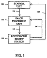
- Fig. 3 shows a block diagram illustrating the operation of the reticle inspection system according to an embodiment of the invention.
- the scanner unit 101 acquires images of the reticle and transmits the image data 104 to the image processing unit 102 for processing.
- the image processing unit 102 performs processing of the image data and detects defects in the reticle. After that, the image processing unit 102 transmits the processed image data 105 of the defective and good dies to the post process and review station 103 for subsequent analysis and display.
- the post process and review station can send control signals 106 and 107 to the image processing unit and the scanner unit. If in the process of image analysis in the post process and review station additional images are needed, such as images from additional focus surfaces, the post process and review sends request 107 to the scanner unit 101 to grab additional images and request 106 to the image processing unit to process those additional images.
Landscapes
- Physics & Mathematics (AREA)
- General Physics & Mathematics (AREA)
- Investigating Materials By The Use Of Optical Means Adapted For Particular Applications (AREA)
- Preparing Plates And Mask In Photomechanical Process (AREA)
- Length Measuring Devices By Optical Means (AREA)
Applications Claiming Priority (2)
| Application Number | Priority Date | Filing Date | Title |
|---|---|---|---|
| US417518 | 1999-10-13 | ||
| US09/417,518 US6268093B1 (en) | 1999-10-13 | 1999-10-13 | Method for reticle inspection using aerial imaging |
Publications (3)
| Publication Number | Publication Date |
|---|---|
| EP1093017A2 true EP1093017A2 (fr) | 2001-04-18 |
| EP1093017A3 EP1093017A3 (fr) | 2004-08-04 |
| EP1093017B1 EP1093017B1 (fr) | 2007-09-19 |
Family
ID=23654328
Family Applications (1)
| Application Number | Title | Priority Date | Filing Date |
|---|---|---|---|
| EP00122146A Expired - Lifetime EP1093017B1 (fr) | 1999-10-13 | 2000-10-12 | Méthode et dispositif d'inspection de réticules utilisant l'imagerie aérienne |
Country Status (4)
| Country | Link |
|---|---|
| US (2) | US6268093B1 (fr) |
| EP (1) | EP1093017B1 (fr) |
| JP (1) | JP4841721B2 (fr) |
| DE (1) | DE60036443T2 (fr) |
Cited By (15)
| Publication number | Priority date | Publication date | Assignee | Title |
|---|---|---|---|---|
| US6633831B2 (en) | 2000-09-20 | 2003-10-14 | Kla Tencor Technologies | Methods and systems for determining a critical dimension and a thin film characteristic of a specimen |
| US6673637B2 (en) | 2000-09-20 | 2004-01-06 | Kla-Tencor Technologies | Methods and systems for determining a presence of macro defects and overlay of a specimen |
| WO2004008244A2 (fr) | 2002-07-15 | 2004-01-22 | Kla-Tencor Technologies Corp. | Qualification de mires, processus de formation de mires ou appareil de formation de mires pour la fabrication de mires microlithographiques |
| US6694284B1 (en) | 2000-09-20 | 2004-02-17 | Kla-Tencor Technologies Corp. | Methods and systems for determining at least four properties of a specimen |
| US6866559B2 (en) | 2002-02-04 | 2005-03-15 | Kla-Tencor Technologies | Windows configurable to be coupled to a process tool or to be disposed within an opening in a polishing pad |
| DE10345783A1 (de) * | 2003-10-01 | 2005-04-21 | Zeiss Carl Sms Gmbh | Optisches Abbildungssystem |
| WO2005076077A3 (fr) * | 2004-02-05 | 2006-04-13 | Koninkl Philips Electronics Nv | Appareil et procede d'inspection de masques |
| WO2006089630A1 (fr) * | 2005-02-25 | 2006-08-31 | Carl Zeiss Sms Gmbh | Procede d'inspection de masques dans le cadre de la conception et de la production de masques |
| US7180658B2 (en) | 2003-02-21 | 2007-02-20 | Kla-Tencor Technologies Corporation | High performance catadioptric imaging system |
| US7236847B2 (en) | 2002-01-16 | 2007-06-26 | Kla-Tencor Technologies Corp. | Systems and methods for closed loop defect reduction |
| EP1269264B1 (fr) * | 2000-02-29 | 2011-03-23 | GlobalFoundries, Inc. | Procédé pour l'analyse d'une méthode de fabrication d'une tranche semi-conductrice |
| US8694929B2 (en) | 2011-07-12 | 2014-04-08 | Carl Zeiss Smt Gmbh | Method and apparatus for the position determination of structures on a mask for microlithography |
| US9659670B2 (en) | 2008-07-28 | 2017-05-23 | Kla-Tencor Corp. | Computer-implemented methods, computer-readable media, and systems for classifying defects detected in a memory device area on a wafer |
| US9865512B2 (en) | 2013-04-08 | 2018-01-09 | Kla-Tencor Corp. | Dynamic design attributes for wafer inspection |
| TWI614569B (zh) * | 2013-04-01 | 2018-02-11 | Kla-Tencor Corporation | 偵測光罩中之缺陷之方法及系統 |
Families Citing this family (152)
| Publication number | Priority date | Publication date | Assignee | Title |
|---|---|---|---|---|
| US6268093B1 (en) * | 1999-10-13 | 2001-07-31 | Applied Materials, Inc. | Method for reticle inspection using aerial imaging |
| US6369888B1 (en) * | 1999-11-17 | 2002-04-09 | Applied Materials, Inc. | Method and apparatus for article inspection including speckle reduction |
| US7095904B2 (en) * | 2000-04-12 | 2006-08-22 | Ultratech, Inc. | Method and apparatus for determining best focus using dark-field imaging |
| US6829380B1 (en) * | 2000-04-28 | 2004-12-07 | Advanced Micro Devices, Inc. | Optimization of OPC design factors utilizing an advanced algorithm on a low voltage CD-SEM system |
| US6735331B1 (en) * | 2000-09-05 | 2004-05-11 | Talia Technology Ltd. | Method and apparatus for early detection and classification of retinal pathologies |
| US7136159B2 (en) * | 2000-09-12 | 2006-11-14 | Kla-Tencor Technologies Corporation | Excimer laser inspection system |
| US6513151B1 (en) * | 2000-09-14 | 2003-01-28 | Advanced Micro Devices, Inc. | Full flow focus exposure matrix analysis and electrical testing for new product mask evaluation |
| US6919957B2 (en) | 2000-09-20 | 2005-07-19 | Kla-Tencor Technologies Corp. | Methods and systems for determining a critical dimension, a presence of defects, and a thin film characteristic of a specimen |
| US7349090B2 (en) | 2000-09-20 | 2008-03-25 | Kla-Tencor Technologies Corp. | Methods and systems for determining a property of a specimen prior to, during, or subsequent to lithography |
| US6782337B2 (en) | 2000-09-20 | 2004-08-24 | Kla-Tencor Technologies Corp. | Methods and systems for determining a critical dimension an a presence of defects on a specimen |
| US7106425B1 (en) | 2000-09-20 | 2006-09-12 | Kla-Tencor Technologies Corp. | Methods and systems for determining a presence of defects and a thin film characteristic of a specimen |
| US6891627B1 (en) | 2000-09-20 | 2005-05-10 | Kla-Tencor Technologies Corp. | Methods and systems for determining a critical dimension and overlay of a specimen |
| US6812045B1 (en) | 2000-09-20 | 2004-11-02 | Kla-Tencor, Inc. | Methods and systems for determining a characteristic of a specimen prior to, during, or subsequent to ion implantation |
| US7130029B2 (en) | 2000-09-20 | 2006-10-31 | Kla-Tencor Technologies Corp. | Methods and systems for determining an adhesion characteristic and a thickness of a specimen |
| US20020120728A1 (en) * | 2000-12-22 | 2002-08-29 | Jason Braatz | Method and apparatus for network-enablement of devices using device intelligence and network architecture |
| US6553559B2 (en) * | 2001-01-05 | 2003-04-22 | International Business Machines Corporation | Method to determine optical proximity correction and assist feature rules which account for variations in mask dimensions |
| US6674522B2 (en) | 2001-05-04 | 2004-01-06 | Kla-Tencor Technologies Corporation | Efficient phase defect detection system and method |
| US7072502B2 (en) * | 2001-06-07 | 2006-07-04 | Applied Materials, Inc. | Alternating phase-shift mask inspection method and apparatus |
| DE10151406B4 (de) * | 2001-10-18 | 2004-04-22 | Infineon Technologies Ag | Photomaske und Verfahren zu dessen Hertellung |
| JP2003130808A (ja) * | 2001-10-29 | 2003-05-08 | Hitachi Ltd | 欠陥検査方法及びその装置 |
| US6976240B2 (en) * | 2001-11-14 | 2005-12-13 | Synopsys Inc. | Simulation using design geometry information |
| US6646281B1 (en) * | 2001-12-28 | 2003-11-11 | Kla-Tencor Corporation | Differential detector coupled with defocus for improved phase defect sensitivity |
| US6906305B2 (en) * | 2002-01-08 | 2005-06-14 | Brion Technologies, Inc. | System and method for aerial image sensing |
| JP3971937B2 (ja) * | 2002-02-18 | 2007-09-05 | 株式会社日立ハイテクノロジーズ | 露光条件監視方法およびその装置並びに半導体デバイスの製造方法 |
| US6727512B2 (en) | 2002-03-07 | 2004-04-27 | Kla-Tencor Technologies Corporation | Method and system for detecting phase defects in lithographic masks and semiconductor wafers |
| US6828542B2 (en) * | 2002-06-07 | 2004-12-07 | Brion Technologies, Inc. | System and method for lithography process monitoring and control |
| US6902855B2 (en) * | 2002-07-15 | 2005-06-07 | Kla-Tencor Technologies | Qualifying patterns, patterning processes, or patterning apparatus in the fabrication of microlithographic patterns |
| US6952256B2 (en) * | 2002-08-30 | 2005-10-04 | Kla-Tencor Technologies Corporation | Optical compensation in high numerical aperture photomask inspection systems for inspecting photomasks through thick pellicles |
| US7046352B1 (en) * | 2002-10-08 | 2006-05-16 | Kla-Tencor Technologies Corporation | Surface inspection system and method using summed light analysis of an inspection surface |
| US7123356B1 (en) | 2002-10-15 | 2006-10-17 | Kla-Tencor Technologies Corp. | Methods and systems for inspecting reticles using aerial imaging and die-to-database detection |
| US7379175B1 (en) * | 2002-10-15 | 2008-05-27 | Kla-Tencor Technologies Corp. | Methods and systems for reticle inspection and defect review using aerial imaging |
| US7027143B1 (en) * | 2002-10-15 | 2006-04-11 | Kla-Tencor Technologies Corp. | Methods and systems for inspecting reticles using aerial imaging at off-stepper wavelengths |
| US6807503B2 (en) * | 2002-11-04 | 2004-10-19 | Brion Technologies, Inc. | Method and apparatus for monitoring integrated circuit fabrication |
| US7457736B2 (en) * | 2002-11-21 | 2008-11-25 | Synopsys, Inc. | Automated creation of metrology recipes |
| US7152219B2 (en) * | 2002-12-10 | 2006-12-19 | Synopsys Inc. | Reference image generation from subject image for photolithography mask analysis |
| DE10258371B4 (de) * | 2002-12-12 | 2004-12-16 | Infineon Technologies Ag | Verfahren zur Inspektion von periodischen Gitterstrukturen auf Lithographiemasken |
| US7133119B1 (en) | 2002-12-17 | 2006-11-07 | Kla-Tencor Technologies Corp. | Systems for simulating high NA and polarization effects in aerial images |
| US7486861B2 (en) * | 2003-01-15 | 2009-02-03 | Negevtech Ltd. | Fiber optical illumination system |
| US6892013B2 (en) * | 2003-01-15 | 2005-05-10 | Negevtech Ltd. | Fiber optical illumination system |
| US7525659B2 (en) * | 2003-01-15 | 2009-04-28 | Negevtech Ltd. | System for detection of water defects |
| JP3787123B2 (ja) * | 2003-02-13 | 2006-06-21 | 株式会社東芝 | 検査方法、プロセッサ及び半導体装置の製造方法 |
| US6950183B2 (en) * | 2003-02-20 | 2005-09-27 | International Business Machines Corporation | Apparatus and method for inspection of photolithographic mask |
| US7053355B2 (en) | 2003-03-18 | 2006-05-30 | Brion Technologies, Inc. | System and method for lithography process monitoring and control |
| JP3960601B2 (ja) * | 2003-03-19 | 2007-08-15 | 株式会社東芝 | エッジ位置ずれ量の算出方法、検証方法、検証プログラム、及び検証システム。 |
| DE10316821A1 (de) * | 2003-04-03 | 2004-10-21 | Infineon Technologies Ag | Verfahren und Vorrichtung zur Korrektur von Abbildungsfehlern eines optischen Systems sowie eine Verwendung der Vorrichtung |
| JP4288415B2 (ja) * | 2003-05-12 | 2009-07-01 | 日本電気株式会社 | レチクル検査装置評価用欠陥データ作り込み方法、システム、装置、及びプログラム |
| US9002497B2 (en) * | 2003-07-03 | 2015-04-07 | Kla-Tencor Technologies Corp. | Methods and systems for inspection of wafers and reticles using designer intent data |
| WO2005017997A1 (fr) * | 2003-08-01 | 2005-02-24 | Applied Materials Israel, Ltd. | Inspection a l'aide d'un faisceau de particules chargees |
| DE10337037B4 (de) * | 2003-08-12 | 2006-02-23 | Infineon Technologies Ag | Verfahren zur Vermessung einer Belichtungsintensität auf einem Wafer |
| US7243331B2 (en) * | 2004-01-28 | 2007-07-10 | Applied Materials, Israel, Ltd. | Method and system for controlling the quality of a reticle |
| WO2005073807A1 (fr) * | 2004-01-29 | 2005-08-11 | Kla-Tencor Technologies Corporation | Procede informatises permettant de detecter les defauts dans les donnees de dessin des reticules |
| US9188974B1 (en) | 2004-02-13 | 2015-11-17 | Kla-Tencor Technologies Corp. | Methods for improved monitor and control of lithography processes |
| WO2006006148A2 (fr) * | 2004-07-12 | 2006-01-19 | Negevtech Ltd. | Procede et appareil d'inspection multimode |
| US20060012781A1 (en) * | 2004-07-14 | 2006-01-19 | Negevtech Ltd. | Programmable spatial filter for wafer inspection |
| JP4904034B2 (ja) | 2004-09-14 | 2012-03-28 | ケーエルエー−テンカー コーポレイション | レチクル・レイアウト・データを評価するための方法、システム及び搬送媒体 |
| JP4645113B2 (ja) * | 2004-09-21 | 2011-03-09 | 日本電気株式会社 | 光検査方法及び光検査装置並びに光検査システム |
| US7095239B2 (en) * | 2004-11-09 | 2006-08-22 | Hitachi Global Storage Technologies Netherlands B.V. | Method for detecting defects that exhibit repetitive patterns |
| US7400390B2 (en) * | 2004-11-29 | 2008-07-15 | Applied Materials, Israel, Ltd. | Inspection system and a method for aerial reticle inspection |
| US7729529B2 (en) * | 2004-12-07 | 2010-06-01 | Kla-Tencor Technologies Corp. | Computer-implemented methods for detecting and/or sorting defects in a design pattern of a reticle |
| US7804993B2 (en) * | 2005-02-28 | 2010-09-28 | Applied Materials South East Asia Pte. Ltd. | Method and apparatus for detecting defects in wafers including alignment of the wafer images so as to induce the same smear in all images |
| US7813541B2 (en) * | 2005-02-28 | 2010-10-12 | Applied Materials South East Asia Pte. Ltd. | Method and apparatus for detecting defects in wafers |
| US20060262295A1 (en) * | 2005-05-20 | 2006-11-23 | Vistec Semiconductor Systems Gmbh | Apparatus and method for inspecting a wafer |
| US7769225B2 (en) * | 2005-08-02 | 2010-08-03 | Kla-Tencor Technologies Corp. | Methods and systems for detecting defects in a reticle design pattern |
| US8041103B2 (en) | 2005-11-18 | 2011-10-18 | Kla-Tencor Technologies Corp. | Methods and systems for determining a position of inspection data in design data space |
| US7676077B2 (en) | 2005-11-18 | 2010-03-09 | Kla-Tencor Technologies Corp. | Methods and systems for utilizing design data in combination with inspection data |
| US7570796B2 (en) | 2005-11-18 | 2009-08-04 | Kla-Tencor Technologies Corp. | Methods and systems for utilizing design data in combination with inspection data |
| EP1984895A4 (fr) * | 2006-02-01 | 2014-09-24 | Applied Materials Israel Ltd | Procede et systeme d'evaluation de variation dans un parametre de motif |
| US8031931B2 (en) | 2006-04-24 | 2011-10-04 | Applied Materials South East Asia Pte. Ltd. | Printed fourier filtering in optical inspection tools |
| DE102007017630B4 (de) * | 2006-05-16 | 2009-08-20 | Vistec Semiconductor Systems Gmbh | Verfahren zum Steigern der Messgenauigkeit beim Bestimmen der Koordinaten von Strukturen auf einem Substrat |
| US7970201B2 (en) * | 2006-07-31 | 2011-06-28 | Applied Materials Israel, Ltd. | Method and system for defect detection |
| US7719674B2 (en) * | 2006-11-28 | 2010-05-18 | Applied Materials South East Asia Pte. Ltd. | Image splitting in optical inspection systems |
| US7714998B2 (en) * | 2006-11-28 | 2010-05-11 | Applied Materials South East Asia Pte. Ltd. | Image splitting in optical inspection systems |
| TWI428686B (zh) * | 2006-12-05 | 2014-03-01 | Hoya Corp | 光罩之檢查裝置、光罩之檢查方法、液晶裝置製造用光罩之製造方法以及圖案轉印方法 |
| WO2008077100A2 (fr) * | 2006-12-19 | 2008-06-26 | Kla-Tencor Corporation | Systèmes et procédés de création de procédures de contrôle |
| WO2008086282A2 (fr) | 2007-01-05 | 2008-07-17 | Kla-Tencor Corporation | Procédés et systèmes pour utiliser des informations électriques dans le cadre de la fabrication d'un dispositif sur une tranche afin d'accomplir une ou plusieurs fonctions liées à des défauts |
| US8335369B2 (en) * | 2007-02-28 | 2012-12-18 | Taiwan Semiconductor Manufacturing Company, Ltd. | Mask defect analysis |
| US7564545B2 (en) * | 2007-03-15 | 2009-07-21 | Kla-Tencor Technologies Corp. | Inspection methods and systems for lithographic masks |
| JP2008249921A (ja) * | 2007-03-30 | 2008-10-16 | Advanced Mask Inspection Technology Kk | レチクル欠陥検査装置およびレチクル欠陥検査方法 |
| US7738093B2 (en) | 2007-05-07 | 2010-06-15 | Kla-Tencor Corp. | Methods for detecting and classifying defects on a reticle |
| US7962863B2 (en) | 2007-05-07 | 2011-06-14 | Kla-Tencor Corp. | Computer-implemented methods, systems, and computer-readable media for determining a model for predicting printability of reticle features on a wafer |
| US8213704B2 (en) | 2007-05-09 | 2012-07-03 | Kla-Tencor Corp. | Methods and systems for detecting defects in a reticle design pattern |
| US7796804B2 (en) | 2007-07-20 | 2010-09-14 | Kla-Tencor Corp. | Methods for generating a standard reference die for use in a die to standard reference die inspection and methods for inspecting a wafer |
| JP5178079B2 (ja) * | 2007-07-23 | 2013-04-10 | 株式会社日立ハイテクノロジーズ | 欠陥検査方法およびその装置 |
| US7711514B2 (en) | 2007-08-10 | 2010-05-04 | Kla-Tencor Technologies Corp. | Computer-implemented methods, carrier media, and systems for generating a metrology sampling plan |
| TWI469235B (zh) | 2007-08-20 | 2015-01-11 | Kla Tencor Corp | 決定實際缺陷是潛在系統性缺陷或潛在隨機缺陷之由電腦實施之方法 |
| JP5039495B2 (ja) * | 2007-10-04 | 2012-10-03 | ルネサスエレクトロニクス株式会社 | マスクブランク検査方法、反射型露光マスクの製造方法、反射型露光方法および半導体集積回路の製造方法 |
| US8139844B2 (en) | 2008-04-14 | 2012-03-20 | Kla-Tencor Corp. | Methods and systems for determining a defect criticality index for defects on wafers |
| US8023102B2 (en) * | 2008-04-18 | 2011-09-20 | International Business Machines Corporation | Test method for determining reticle transmission stability |
| JP6185693B2 (ja) * | 2008-06-11 | 2017-08-23 | ケーエルエー−テンカー・コーポレーションKla−Tencor Corporation | ウェーハー上の設計欠陥および工程欠陥の検出、ウェーハー上の欠陥の精査、設計内の1つ以上の特徴を工程監視特徴として使用するための選択、またはそのいくつかの組み合わせのためのシステムおよび方法 |
| DE102008048660B4 (de) * | 2008-09-22 | 2015-06-18 | Carl Zeiss Sms Gmbh | Verfahren und Vorrichtung zur Vermessung von Strukturen auf Photolithographiemasken |
| NL2003678A (en) * | 2008-12-17 | 2010-06-21 | Asml Holding Nv | Euv mask inspection system. |
| NL2003658A (en) * | 2008-12-31 | 2010-07-01 | Asml Holding Nv | Euv mask inspection. |
| US8605275B2 (en) * | 2009-01-26 | 2013-12-10 | Kla-Tencor Corp. | Detecting defects on a wafer |
| US8223327B2 (en) | 2009-01-26 | 2012-07-17 | Kla-Tencor Corp. | Systems and methods for detecting defects on a wafer |
| US8775101B2 (en) | 2009-02-13 | 2014-07-08 | Kla-Tencor Corp. | Detecting defects on a wafer |
| US8204297B1 (en) | 2009-02-27 | 2012-06-19 | Kla-Tencor Corp. | Methods and systems for classifying defects detected on a reticle |
| US8327298B2 (en) | 2009-02-27 | 2012-12-04 | Applied Materials Israel, Ltd. | System and method for evaluating error sources associated with a mask |
| US8112241B2 (en) | 2009-03-13 | 2012-02-07 | Kla-Tencor Corp. | Methods and systems for generating an inspection process for a wafer |
| JP5872452B2 (ja) * | 2009-04-13 | 2016-03-01 | エーエスエムエル ホールディング エヌ.ブイ. | フーリエフィルタリングおよびイメージ比較を用いるマスク検査システム及び方法、並びにリソグラフィシステム |
| DE102010009022B4 (de) | 2010-02-22 | 2019-10-24 | Carl Zeiss Smt Gmbh | Beleuchtungssystem sowie Projektionsobjektiv einer Maskeninspektionsanlage |
| US8781781B2 (en) | 2010-07-30 | 2014-07-15 | Kla-Tencor Corp. | Dynamic care areas |
| TWI497055B (zh) * | 2010-07-30 | 2015-08-21 | Hoya股份有限公司 | 透過率測定裝置、光罩之透過率檢查裝置、透過率檢查方法、光罩製造方法、圖案轉印方法、光罩製品 |
| EP2434345B1 (fr) * | 2010-09-27 | 2013-07-03 | Imec | Procédé et système d'évaluation de la planéité de masques EUV |
| US8810646B2 (en) * | 2010-10-12 | 2014-08-19 | Kla-Tencor Corporation | Focus offset contamination inspection |
| US9576349B2 (en) * | 2010-12-20 | 2017-02-21 | Microsoft Technology Licensing, Llc | Techniques for atmospheric and solar correction of aerial images |
| US9170211B2 (en) | 2011-03-25 | 2015-10-27 | Kla-Tencor Corp. | Design-based inspection using repeating structures |
| US9494856B1 (en) * | 2011-06-07 | 2016-11-15 | Hermes Microvision, Inc. | Method and system for fast inspecting defects |
| US9087367B2 (en) | 2011-09-13 | 2015-07-21 | Kla-Tencor Corp. | Determining design coordinates for wafer defects |
| US8831334B2 (en) | 2012-01-20 | 2014-09-09 | Kla-Tencor Corp. | Segmentation for wafer inspection |
| US8578309B2 (en) * | 2012-01-31 | 2013-11-05 | Taiwan Semiconductor Manufacturing Co., Ltd. | Format conversion from value change dump (VCD) to universal verification methodology (UVM) |
| US9281748B2 (en) | 2012-03-02 | 2016-03-08 | Lenovo Enterprise Solutions (Singapore) Pte. Ltd. | Operating a DC-DC converter |
| US8901897B2 (en) | 2012-03-02 | 2014-12-02 | International Business Machines Corporation | Operating a DC-DC converter |
| US8826200B2 (en) | 2012-05-25 | 2014-09-02 | Kla-Tencor Corp. | Alteration for wafer inspection |
| US8984453B2 (en) * | 2012-06-28 | 2015-03-17 | Applied Materials Israel, Ltd. | Method and system for creation of binary spatial filters |
| US9189844B2 (en) | 2012-10-15 | 2015-11-17 | Kla-Tencor Corp. | Detecting defects on a wafer using defect-specific information |
| US8965102B2 (en) | 2012-11-09 | 2015-02-24 | Taiwan Semiconductor Manufacturing Company, Ltd. | System and method for defect analysis of a substrate |
| US8754669B2 (en) * | 2012-11-09 | 2014-06-17 | International Business Machines Corporation | Dynamic impedance matching for improved transient performance in a direct current-to-direct current (‘DC/DC’) converter for delivering a load to an electrical component |
| US20140151580A1 (en) * | 2012-11-30 | 2014-06-05 | Kla-Tencor Corporation | Methods of using polished silicon wafer strips for euv homogenizer |
| US9053527B2 (en) | 2013-01-02 | 2015-06-09 | Kla-Tencor Corp. | Detecting defects on a wafer |
| US9134254B2 (en) | 2013-01-07 | 2015-09-15 | Kla-Tencor Corp. | Determining a position of inspection system output in design data space |
| US9311698B2 (en) | 2013-01-09 | 2016-04-12 | Kla-Tencor Corp. | Detecting defects on a wafer using template image matching |
| US9092846B2 (en) | 2013-02-01 | 2015-07-28 | Kla-Tencor Corp. | Detecting defects on a wafer using defect-specific and multi-channel information |
| US9607371B2 (en) | 2013-04-01 | 2017-03-28 | Kla-Tencor Corporation | Mesoscopic defect detection for reticle inspection |
| US9310320B2 (en) | 2013-04-15 | 2016-04-12 | Kla-Tencor Corp. | Based sampling and binning for yield critical defects |
| WO2014186476A2 (fr) * | 2013-05-14 | 2014-11-20 | Kla-Tencor Corporation | Inspection intégrée à passages multiples |
| DE102013212613B4 (de) | 2013-06-28 | 2015-07-23 | Carl Zeiss Sms Gmbh | Beleuchtungsoptik für ein Metrologiesystem sowie Metrologiesystem mit einer derartigen Beleuchtungsoptik |
| US9236347B2 (en) | 2013-10-09 | 2016-01-12 | Lenovo Enterprise Solutions (Singapore) Pte. Ltd. | Operating and manufacturing a DC-DC converter |
| US20150204799A1 (en) * | 2014-01-21 | 2015-07-23 | International Business Machines Corporation | Computer-based defect root cause and yield impact determination in layered device manufacturing for products and services |
| US9218446B1 (en) * | 2014-06-13 | 2015-12-22 | Globalfoundries Inc. | Optimization of integrated circuits for a reticle transmission process window using multiple fill cells |
| US9219422B1 (en) | 2014-08-21 | 2015-12-22 | Lenovo Enterprise Solutions (Singapore) Pte. Ltd. | Operating a DC-DC converter including a coupled inductor formed of a magnetic core and a conductive sheet |
| KR102021450B1 (ko) | 2014-09-22 | 2019-11-04 | 에이에스엠엘 네델란즈 비.브이. | 공정 윈도우 식별자 |
| US9379619B2 (en) | 2014-10-21 | 2016-06-28 | Lenovo Enterprise Solutions (Singapore) Pte. Ltd. | Dividing a single phase pulse-width modulation signal into a plurality of phases |
| US9618539B2 (en) | 2015-05-28 | 2017-04-11 | Lenovo Enterprise Solutions (Singapore) Pte. Ltd. | Sensing current of a DC-DC converter |
| JP6640482B2 (ja) * | 2015-07-31 | 2020-02-05 | 株式会社ニューフレアテクノロジー | パターン検査装置及びパターン検査方法 |
| JP6527808B2 (ja) | 2015-10-27 | 2019-06-05 | 株式会社ニューフレアテクノロジー | 検査方法および検査装置 |
| JP6759053B2 (ja) | 2016-10-26 | 2020-09-23 | 株式会社ニューフレアテクノロジー | 偏光イメージ取得装置、パターン検査装置、偏光イメージ取得方法、及びパターン検査方法 |
| JP6917208B2 (ja) | 2017-06-19 | 2021-08-11 | 株式会社ニューフレアテクノロジー | 偏光イメージ取得装置、パターン検査装置、偏光イメージ取得方法、及びパターン検査方法 |
| US10753729B2 (en) | 2018-10-02 | 2020-08-25 | Saudi Arabian Oil Company | Photonic sensing analytical device |
| JP6815469B2 (ja) * | 2019-11-13 | 2021-01-20 | 株式会社ニューフレアテクノロジー | パターン検査装置及びパターン検査方法 |
| CN113466259B (zh) * | 2020-03-31 | 2023-02-17 | 上海微电子装备(集团)股份有限公司 | 金属掩模检测装置、光源标定方法及装置和维护标定方法 |
| DE102020208045A1 (de) * | 2020-06-29 | 2021-12-30 | Carl Zeiss Smt Gmbh | Verfahren zur Ermittlung eines Bildes eines Objekts |
| JP7554064B2 (ja) * | 2020-06-30 | 2024-09-19 | 株式会社ヴィーネックス | 異物・欠陥検査装置、異物・欠陥検査における画像生成装置、及び異物・欠陥検査方法 |
| US11435298B2 (en) * | 2020-07-24 | 2022-09-06 | Hewlett Packard Enterprise Development Lp | Circuit board anomaly indication |
| KR102869735B1 (ko) * | 2020-11-03 | 2025-10-13 | 세메스 주식회사 | 마스크 보관 장치 |
| WO2022113852A1 (fr) * | 2020-11-27 | 2022-06-02 | 富士フイルム株式会社 | Dispositif d'inspection visuelle, procédé d'inspection visuelle et programme d'inspection visuelle |
| KR20240018489A (ko) * | 2021-06-09 | 2024-02-13 | 에이에스엠엘 네델란즈 비.브이. | 애퍼처 아포디제이션을 갖는 구조적 조명을 이용한 레티클 입자 검출을 위한 검사 시스템 |
| CN113834818A (zh) * | 2021-09-15 | 2021-12-24 | 江苏维普光电科技有限公司 | 基于频闪切换照明的掩膜版缺陷检测方法及系统 |
| CN114264662B (zh) * | 2021-12-10 | 2024-03-08 | 上海市东方海事工程技术有限公司 | 一种钢轨表面视觉检测方法和装置 |
| US12596262B2 (en) * | 2022-06-27 | 2026-04-07 | Applied Materials Israel Ltd. | Light source system and method |
| CN118818881A (zh) * | 2023-04-19 | 2024-10-22 | 联华电子股份有限公司 | 光学邻近效应校正的切分方法与图案化的方法 |
| DE102024118199A1 (de) * | 2024-06-27 | 2025-12-31 | Carl Zeiss Smt Gmbh | Verfahren und System zum Detektieren von druckenden Defekten in einer Fotolithografiemaske |
| DE102024118195A1 (de) * | 2024-06-27 | 2025-07-10 | Carl Zeiss Smt Gmbh | Verfahren und System zum Bewerten der Qualität einer Fotolithografiemaske |
Family Cites Families (38)
| Publication number | Priority date | Publication date | Assignee | Title |
|---|---|---|---|---|
| JPS5233523B1 (fr) | 1971-02-18 | 1977-08-29 | ||
| JPS5371563A (en) * | 1976-12-08 | 1978-06-26 | Hitachi Ltd | Automatic inspection correcting method for mask |
| US4247203A (en) * | 1978-04-03 | 1981-01-27 | Kla Instrument Corporation | Automatic photomask inspection system and apparatus |
| US4926489A (en) | 1983-03-11 | 1990-05-15 | Kla Instruments Corporation | Reticle inspection system |
| US4595289A (en) * | 1984-01-25 | 1986-06-17 | At&T Bell Laboratories | Inspection system utilizing dark-field illumination |
| JPS6235618A (ja) * | 1985-08-09 | 1987-02-16 | Hitachi Ltd | 欠陥検査装置 |
| US4922308A (en) * | 1986-06-27 | 1990-05-01 | Hitachi, Ltd. | Method of and apparatus for detecting foreign substance |
| US5210635A (en) | 1989-04-17 | 1993-05-11 | Dainippon Screen Mfg. Co., Ltd. | Multibeam scanning system |
| US5576829A (en) * | 1990-10-08 | 1996-11-19 | Nikon Corporation | Method and apparatus for inspecting a phase-shifted mask |
| US5563702A (en) | 1991-08-22 | 1996-10-08 | Kla Instruments Corporation | Automated photomask inspection apparatus and method |
| DE69208413T2 (de) * | 1991-08-22 | 1996-11-14 | Kla Instr Corp | Gerät zur automatischen Prüfung von Photomaske |
| JP2655215B2 (ja) * | 1991-11-18 | 1997-09-17 | 三菱電機株式会社 | フォトマスクのパターン欠陥修正方法 |
| JPH05296937A (ja) * | 1992-04-23 | 1993-11-12 | Nikon Corp | 異物検査装置 |
| JP2667940B2 (ja) | 1992-04-27 | 1997-10-27 | 三菱電機株式会社 | マスク検査方法およびマスク検出装置 |
| JP3328323B2 (ja) * | 1992-07-20 | 2002-09-24 | 株式会社日立製作所 | 位相シフトマスクの製造方法および半導体集積回路装置の製造方法 |
| JPH0728226A (ja) * | 1993-04-30 | 1995-01-31 | Internatl Business Mach Corp <Ibm> | 領域的イメージを測定する装置及び方法 |
| KR0184992B1 (ko) * | 1995-01-26 | 1999-05-15 | 가네꼬 히사시 | 음극 선관 블랙 매트릭스층을 위한 구멍 크기 측정 시스템 |
| US6148097A (en) * | 1995-06-07 | 2000-11-14 | Asahi Kogaku Kogyo Kabushiki Kaisha | Optical member inspecting apparatus and method of inspection thereof |
| US5744381A (en) * | 1995-03-13 | 1998-04-28 | Kabushiki Kaisha Toshiba | Method of inspecting a pattern formed on a sample for a defect, and an apparatus thereof |
| US5838433A (en) | 1995-04-19 | 1998-11-17 | Nikon Corporation | Apparatus for detecting defects on a mask |
| IL118872A (en) * | 1996-07-16 | 2000-06-01 | Orbot Instr Ltd | Optical inspection method and apparatus |
| US5795688A (en) | 1996-08-14 | 1998-08-18 | Micron Technology, Inc. | Process for detecting defects in photomasks through aerial image comparisons |
| JPH1078648A (ja) | 1996-09-04 | 1998-03-24 | Toshiba Corp | 位相シフトマスク検査装置 |
| US6075883A (en) * | 1996-11-12 | 2000-06-13 | Robotic Vision Systems, Inc. | Method and system for imaging an object or pattern |
| US6025905A (en) * | 1996-12-31 | 2000-02-15 | Cognex Corporation | System for obtaining a uniform illumination reflectance image during periodic structured illumination |
| US6078738A (en) * | 1997-05-08 | 2000-06-20 | Lsi Logic Corporation | Comparing aerial image to SEM of photoresist or substrate pattern for masking process characterization |
| US6016357A (en) * | 1997-06-16 | 2000-01-18 | International Business Machines Corporation | Feedback method to repair phase shift masks |
| US5965306A (en) * | 1997-10-15 | 1999-10-12 | International Business Machines Corporation | Method of determining the printability of photomask defects |
| US6072898A (en) * | 1998-01-16 | 2000-06-06 | Beaty; Elwin M. | Method and apparatus for three dimensional inspection of electronic components |
| US6091845A (en) * | 1998-02-24 | 2000-07-18 | Micron Technology, Inc. | Inspection technique of photomask |
| US6018392A (en) * | 1998-10-23 | 2000-01-25 | Taiwan Semiconductor Manufacturing Company | Apparatus and method for inspecting phase shifting masks |
| US6124924A (en) * | 1998-12-24 | 2000-09-26 | Applied Materials, Inc. | Focus error correction method and apparatus |
| JP3848006B2 (ja) * | 1999-03-15 | 2006-11-22 | 株式会社東芝 | マスク欠陥修正方法 |
| JP3544892B2 (ja) | 1999-05-12 | 2004-07-21 | 株式会社東京精密 | 外観検査方法及び装置 |
| US6327033B1 (en) | 1999-06-21 | 2001-12-04 | International Business Machines Corporation | Detection of phase defects on photomasks by differential imaging |
| US6466315B1 (en) * | 1999-09-03 | 2002-10-15 | Applied Materials, Inc. | Method and system for reticle inspection by photolithography simulation |
| US6268093B1 (en) * | 1999-10-13 | 2001-07-31 | Applied Materials, Inc. | Method for reticle inspection using aerial imaging |
| US6674522B2 (en) * | 2001-05-04 | 2004-01-06 | Kla-Tencor Technologies Corporation | Efficient phase defect detection system and method |
-
1999
- 1999-10-13 US US09/417,518 patent/US6268093B1/en not_active Expired - Lifetime
-
2000
- 2000-10-12 EP EP00122146A patent/EP1093017B1/fr not_active Expired - Lifetime
- 2000-10-12 DE DE60036443T patent/DE60036443T2/de not_active Expired - Fee Related
- 2000-10-13 JP JP2000351938A patent/JP4841721B2/ja not_active Expired - Lifetime
-
2001
- 2001-05-08 US US09/851,779 patent/US7133548B2/en not_active Expired - Lifetime
Cited By (29)
| Publication number | Priority date | Publication date | Assignee | Title |
|---|---|---|---|---|
| EP1269264B1 (fr) * | 2000-02-29 | 2011-03-23 | GlobalFoundries, Inc. | Procédé pour l'analyse d'une méthode de fabrication d'une tranche semi-conductrice |
| US6633831B2 (en) | 2000-09-20 | 2003-10-14 | Kla Tencor Technologies | Methods and systems for determining a critical dimension and a thin film characteristic of a specimen |
| US6673637B2 (en) | 2000-09-20 | 2004-01-06 | Kla-Tencor Technologies | Methods and systems for determining a presence of macro defects and overlay of a specimen |
| US6694284B1 (en) | 2000-09-20 | 2004-02-17 | Kla-Tencor Technologies Corp. | Methods and systems for determining at least four properties of a specimen |
| US7236847B2 (en) | 2002-01-16 | 2007-06-26 | Kla-Tencor Technologies Corp. | Systems and methods for closed loop defect reduction |
| US6884146B2 (en) | 2002-02-04 | 2005-04-26 | Kla-Tencor Technologies Corp. | Systems and methods for characterizing a polishing process |
| US7332438B2 (en) | 2002-02-04 | 2008-02-19 | Kla-Tencor Technologies Corp. | Methods and systems for monitoring a parameter of a measurement device during polishing, damage to a specimen during polishing, or a characteristic of a polishing pad or tool |
| US6866559B2 (en) | 2002-02-04 | 2005-03-15 | Kla-Tencor Technologies | Windows configurable to be coupled to a process tool or to be disposed within an opening in a polishing pad |
| US6935922B2 (en) | 2002-02-04 | 2005-08-30 | Kla-Tencor Technologies Corp. | Methods and systems for generating a two-dimensional map of a characteristic at relative or absolute locations of measurement spots on a specimen during polishing |
| US8831767B2 (en) | 2002-02-04 | 2014-09-09 | Kla-Tencor Technologies Corp. | Methods and systems for monitoring a parameter of a measurement device during polishing, damage to a specimen during polishing, or a characteristic of a polishing pad or tool |
| US7030018B2 (en) | 2002-02-04 | 2006-04-18 | Kla-Tencor Technologies Corp. | Methods and systems for monitoring a parameter of a measurement device during polishing, damage to a specimen during polishing, or a characteristic of a polishing pad or tool |
| US7052369B2 (en) | 2002-02-04 | 2006-05-30 | Kla-Tencor Technologies Corp. | Methods and systems for detecting a presence of blobs on a specimen during a polishing process |
| US8010222B2 (en) | 2002-02-04 | 2011-08-30 | Kla-Tencor Technologies Corp. | Methods and systems for monitoring a parameter of a measurement device during polishing, damage to a specimen during polishing, or a characteristic of a polishing pad or tool |
| US7175503B2 (en) | 2002-02-04 | 2007-02-13 | Kla-Tencor Technologies Corp. | Methods and systems for determining a characteristic of polishing within a zone on a specimen from combined output signals of an eddy current device |
| KR100979484B1 (ko) * | 2002-07-15 | 2010-09-02 | 케이엘에이-텐코 코포레이션 | 다른 리소그래픽 과정 변수들을 위한 레티클의 가상 이미지를 얻는 것을 포함하는 결점 조사 방법 |
| US7418124B2 (en) | 2002-07-15 | 2008-08-26 | Kla-Tencor Technologies Corp. | Qualifying patterns, patterning processes, or patterning apparatus in the fabrication of microlithographic patterns |
| WO2004008244A3 (fr) * | 2002-07-15 | 2004-07-29 | Kla Tencor Tech Corp | Qualification de mires, processus de formation de mires ou appareil de formation de mires pour la fabrication de mires microlithographiques |
| WO2004008244A2 (fr) | 2002-07-15 | 2004-01-22 | Kla-Tencor Technologies Corp. | Qualification de mires, processus de formation de mires ou appareil de formation de mires pour la fabrication de mires microlithographiques |
| US7180658B2 (en) | 2003-02-21 | 2007-02-20 | Kla-Tencor Technologies Corporation | High performance catadioptric imaging system |
| US7679842B2 (en) | 2003-02-21 | 2010-03-16 | Kla-Tencor Technologies Corporation | High performance catadioptric imaging system |
| DE10345783A1 (de) * | 2003-10-01 | 2005-04-21 | Zeiss Carl Sms Gmbh | Optisches Abbildungssystem |
| WO2005076077A3 (fr) * | 2004-02-05 | 2006-04-13 | Koninkl Philips Electronics Nv | Appareil et procede d'inspection de masques |
| JP2009521708A (ja) * | 2005-02-25 | 2009-06-04 | カール ツアイス エスエムエス ゲゼルシャフト ミット ベシュレンクテル ハフツング | マスク設計及びマスク製造におけるマスク検査のための方法 |
| US8705838B2 (en) | 2005-02-25 | 2014-04-22 | Carl Zeiss Sms Gmbh | Method for mask inspection for mask design and mask production |
| WO2006089630A1 (fr) * | 2005-02-25 | 2006-08-31 | Carl Zeiss Sms Gmbh | Procede d'inspection de masques dans le cadre de la conception et de la production de masques |
| US9659670B2 (en) | 2008-07-28 | 2017-05-23 | Kla-Tencor Corp. | Computer-implemented methods, computer-readable media, and systems for classifying defects detected in a memory device area on a wafer |
| US8694929B2 (en) | 2011-07-12 | 2014-04-08 | Carl Zeiss Smt Gmbh | Method and apparatus for the position determination of structures on a mask for microlithography |
| TWI614569B (zh) * | 2013-04-01 | 2018-02-11 | Kla-Tencor Corporation | 偵測光罩中之缺陷之方法及系統 |
| US9865512B2 (en) | 2013-04-08 | 2018-01-09 | Kla-Tencor Corp. | Dynamic design attributes for wafer inspection |
Also Published As
| Publication number | Publication date |
|---|---|
| EP1093017B1 (fr) | 2007-09-19 |
| DE60036443T2 (de) | 2008-06-26 |
| JP2001235853A (ja) | 2001-08-31 |
| DE60036443D1 (de) | 2007-10-31 |
| US20010019625A1 (en) | 2001-09-06 |
| US7133548B2 (en) | 2006-11-07 |
| JP4841721B2 (ja) | 2011-12-21 |
| EP1093017A3 (fr) | 2004-08-04 |
| US6268093B1 (en) | 2001-07-31 |
Similar Documents
| Publication | Publication Date | Title |
|---|---|---|
| EP1093017B1 (fr) | Méthode et dispositif d'inspection de réticules utilisant l'imagerie aérienne | |
| US7072502B2 (en) | Alternating phase-shift mask inspection method and apparatus | |
| US7379175B1 (en) | Methods and systems for reticle inspection and defect review using aerial imaging | |
| US7027143B1 (en) | Methods and systems for inspecting reticles using aerial imaging at off-stepper wavelengths | |
| US6091845A (en) | Inspection technique of photomask | |
| US7123356B1 (en) | Methods and systems for inspecting reticles using aerial imaging and die-to-database detection | |
| US9417191B2 (en) | Using reflected and transmission maps to detect reticle degradation | |
| CN101315518B (zh) | 光掩模检查及制造方法、电子部件制造方法 | |
| CN109659245B (zh) | 监测光掩模缺陷率的改变 | |
| US7469057B2 (en) | System and method for inspecting errors on a wafer | |
| KR102079420B1 (ko) | 통합된 멀티 패스 검사 | |
| US6023328A (en) | Photomask inspection method and apparatus | |
| KR20170015249A (ko) | 패턴 검사 장치 및 패턴 검사 방법 | |
| US6999611B1 (en) | Reticle defect detection using simulation | |
| US7400390B2 (en) | Inspection system and a method for aerial reticle inspection | |
| JPH04321047A (ja) | フォトマスク検査装置及びフォトマスク検査方法 | |
| CN101446753B (zh) | 光掩模及其检查装置、方法、以及制造方法、图案转写方法 | |
| JP2011169743A (ja) | 検査装置および検査方法 | |
| JPH04328548A (ja) | フォトマスクの検査方法および装置 | |
| JP2000193596A (ja) | 検査方法 | |
| CN116754580B (zh) | 半导体样品制造的掩模检查 | |
| JP2019086481A (ja) | パターン検査装置及びパターン検査方法 | |
| JPH05218159A (ja) | 共通欠陥検査方法 | |
| Rosenbusch et al. | Aerial-image based inspeciton of AAPSM for 193-nm lithography generation |
Legal Events
| Date | Code | Title | Description |
|---|---|---|---|
| PUAI | Public reference made under article 153(3) epc to a published international application that has entered the european phase |
Free format text: ORIGINAL CODE: 0009012 |
|
| AK | Designated contracting states |
Kind code of ref document: A2 Designated state(s): AT BE CH CY DE DK ES FI FR GB GR IE IT LI LU MC NL PT SE |
|
| AX | Request for extension of the european patent |
Free format text: AL;LT;LV;MK;RO;SI |
|
| PUAL | Search report despatched |
Free format text: ORIGINAL CODE: 0009013 |
|
| RIC1 | Information provided on ipc code assigned before grant |
Ipc: 7G 03F 1/00 B Ipc: 7G 03F 7/20 A |
|
| AK | Designated contracting states |
Kind code of ref document: A3 Designated state(s): AT BE CH CY DE DK ES FI FR GB GR IE IT LI LU MC NL PT SE |
|
| AX | Request for extension of the european patent |
Extension state: AL LT LV MK RO SI |
|
| 17P | Request for examination filed |
Effective date: 20050202 |
|
| AKX | Designation fees paid |
Designated state(s): DE |
|
| 17Q | First examination report despatched |
Effective date: 20050603 |
|
| RBV | Designated contracting states (corrected) |
Designated state(s): DE |
|
| GRAC | Information related to communication of intention to grant a patent modified |
Free format text: ORIGINAL CODE: EPIDOSCIGR1 |
|
| GRAP | Despatch of communication of intention to grant a patent |
Free format text: ORIGINAL CODE: EPIDOSNIGR1 |
|
| GRAS | Grant fee paid |
Free format text: ORIGINAL CODE: EPIDOSNIGR3 |
|
| 17Q | First examination report despatched |
Effective date: 20050603 |
|
| GRAA | (expected) grant |
Free format text: ORIGINAL CODE: 0009210 |
|
| AK | Designated contracting states |
Kind code of ref document: B1 Designated state(s): DE |
|
| REF | Corresponds to: |
Ref document number: 60036443 Country of ref document: DE Date of ref document: 20071031 Kind code of ref document: P |
|
| PLBE | No opposition filed within time limit |
Free format text: ORIGINAL CODE: 0009261 |
|
| STAA | Information on the status of an ep patent application or granted ep patent |
Free format text: STATUS: NO OPPOSITION FILED WITHIN TIME LIMIT |
|
| 26N | No opposition filed |
Effective date: 20080620 |
|
| PGFP | Annual fee paid to national office [announced via postgrant information from national office to epo] |
Ref country code: DE Payment date: 20081031 Year of fee payment: 9 |
|
| PG25 | Lapsed in a contracting state [announced via postgrant information from national office to epo] |
Ref country code: DE Free format text: LAPSE BECAUSE OF NON-PAYMENT OF DUE FEES Effective date: 20100501 |