EP1094437A2 - Dispositif d'affichage à cristaux liquides doté de caractéristiques améliorées de réponse - Google Patents
Dispositif d'affichage à cristaux liquides doté de caractéristiques améliorées de réponse Download PDFInfo
- Publication number
- EP1094437A2 EP1094437A2 EP00119134A EP00119134A EP1094437A2 EP 1094437 A2 EP1094437 A2 EP 1094437A2 EP 00119134 A EP00119134 A EP 00119134A EP 00119134 A EP00119134 A EP 00119134A EP 1094437 A2 EP1094437 A2 EP 1094437A2
- Authority
- EP
- European Patent Office
- Prior art keywords
- gray
- display data
- display
- liquid crystal
- scale voltage
- Prior art date
- Legal status (The legal status is an assumption and is not a legal conclusion. Google has not performed a legal analysis and makes no representation as to the accuracy of the status listed.)
- Granted
Links
Images



Classifications
-
- G—PHYSICS
- G09—EDUCATION; CRYPTOGRAPHY; DISPLAY; ADVERTISING; SEALS
- G09G—ARRANGEMENTS OR CIRCUITS FOR CONTROL OF INDICATING DEVICES USING STATIC MEANS TO PRESENT VARIABLE INFORMATION
- G09G3/00—Control arrangements or circuits, of interest only in connection with visual indicators other than cathode-ray tubes
- G09G3/20—Control arrangements or circuits, of interest only in connection with visual indicators other than cathode-ray tubes for presentation of an assembly of a number of characters, e.g. a page, by composing the assembly by combination of individual elements arranged in a matrix no fixed position being assigned to or needed to be assigned to the individual characters or partial characters
- G09G3/34—Control arrangements or circuits, of interest only in connection with visual indicators other than cathode-ray tubes for presentation of an assembly of a number of characters, e.g. a page, by composing the assembly by combination of individual elements arranged in a matrix no fixed position being assigned to or needed to be assigned to the individual characters or partial characters by control of light from an independent source
- G09G3/36—Control arrangements or circuits, of interest only in connection with visual indicators other than cathode-ray tubes for presentation of an assembly of a number of characters, e.g. a page, by composing the assembly by combination of individual elements arranged in a matrix no fixed position being assigned to or needed to be assigned to the individual characters or partial characters by control of light from an independent source using liquid crystals
-
- G—PHYSICS
- G09—EDUCATION; CRYPTOGRAPHY; DISPLAY; ADVERTISING; SEALS
- G09G—ARRANGEMENTS OR CIRCUITS FOR CONTROL OF INDICATING DEVICES USING STATIC MEANS TO PRESENT VARIABLE INFORMATION
- G09G3/00—Control arrangements or circuits, of interest only in connection with visual indicators other than cathode-ray tubes
- G09G3/20—Control arrangements or circuits, of interest only in connection with visual indicators other than cathode-ray tubes for presentation of an assembly of a number of characters, e.g. a page, by composing the assembly by combination of individual elements arranged in a matrix no fixed position being assigned to or needed to be assigned to the individual characters or partial characters
- G09G3/34—Control arrangements or circuits, of interest only in connection with visual indicators other than cathode-ray tubes for presentation of an assembly of a number of characters, e.g. a page, by composing the assembly by combination of individual elements arranged in a matrix no fixed position being assigned to or needed to be assigned to the individual characters or partial characters by control of light from an independent source
- G09G3/36—Control arrangements or circuits, of interest only in connection with visual indicators other than cathode-ray tubes for presentation of an assembly of a number of characters, e.g. a page, by composing the assembly by combination of individual elements arranged in a matrix no fixed position being assigned to or needed to be assigned to the individual characters or partial characters by control of light from an independent source using liquid crystals
- G09G3/3611—Control of matrices with row and column drivers
-
- G—PHYSICS
- G09—EDUCATION; CRYPTOGRAPHY; DISPLAY; ADVERTISING; SEALS
- G09G—ARRANGEMENTS OR CIRCUITS FOR CONTROL OF INDICATING DEVICES USING STATIC MEANS TO PRESENT VARIABLE INFORMATION
- G09G2320/00—Control of display operating conditions
- G09G2320/02—Improving the quality of display appearance
-
- G—PHYSICS
- G09—EDUCATION; CRYPTOGRAPHY; DISPLAY; ADVERTISING; SEALS
- G09G—ARRANGEMENTS OR CIRCUITS FOR CONTROL OF INDICATING DEVICES USING STATIC MEANS TO PRESENT VARIABLE INFORMATION
- G09G2320/00—Control of display operating conditions
- G09G2320/02—Improving the quality of display appearance
- G09G2320/0252—Improving the response speed
-
- G—PHYSICS
- G09—EDUCATION; CRYPTOGRAPHY; DISPLAY; ADVERTISING; SEALS
- G09G—ARRANGEMENTS OR CIRCUITS FOR CONTROL OF INDICATING DEVICES USING STATIC MEANS TO PRESENT VARIABLE INFORMATION
- G09G2320/00—Control of display operating conditions
- G09G2320/02—Improving the quality of display appearance
- G09G2320/0261—Improving the quality of display appearance in the context of movement of objects on the screen or movement of the observer relative to the screen
-
- G—PHYSICS
- G09—EDUCATION; CRYPTOGRAPHY; DISPLAY; ADVERTISING; SEALS
- G09G—ARRANGEMENTS OR CIRCUITS FOR CONTROL OF INDICATING DEVICES USING STATIC MEANS TO PRESENT VARIABLE INFORMATION
- G09G2340/00—Aspects of display data processing
- G09G2340/16—Determination of a pixel data signal depending on the signal applied in the previous frame
-
- G—PHYSICS
- G09—EDUCATION; CRYPTOGRAPHY; DISPLAY; ADVERTISING; SEALS
- G09G—ARRANGEMENTS OR CIRCUITS FOR CONTROL OF INDICATING DEVICES USING STATIC MEANS TO PRESENT VARIABLE INFORMATION
- G09G5/00—Control arrangements or circuits for visual indicators common to cathode-ray tube indicators and other visual indicators
- G09G5/36—Control arrangements or circuits for visual indicators common to cathode-ray tube indicators and other visual indicators characterised by the display of a graphic pattern, e.g. using an all-points-addressable [APA] memory
- G09G5/39—Control of the bit-mapped memory
Definitions
- This invention relates to a liquid crystal display device. More particularly, this invention relates to a driving circuit that improves response as a luminance change time of a liquid crystal.
- This response formula of the liquid crystal suggests that in order to improve the response by contriving the liquid crystal material, the viscosity parameter ⁇ i of the liquid crystal material needs to be made small.
- the liquid crystal cell gap d needs to be reduced.
- a driving voltage (a liquid crystal applied voltage) needs to be increased.
- a liquid crystal driving circuit for generating the driving voltage must be improved. Since the liquid crystal driving circuit generally comprises an integrated circuit, this integrated circuit must be accomplished by means of a high voltage process, and results in the high cost of production. Further, to improve the viscosity parameter of the liquid crystal and the cell gap, the production process of the liquid crystal must be changed drastically, and such a modification also results in a high cost of production.
- the response of the liquid crystal cannot be improved. Even when any change occurs in the display content, the content displayed in a preceding frame is displayed as an after-image rasidual image (residual image). As a result, when a figure such as a rectangle, displayed on the liquid crystal panel moves, the rectangle moves with a blurred edge, deteriorating image quality.
- the object of the present invention is to provide a liquid crystal display device that improves the response from the point of time at which a signal driving circuit applies a gray-scale voltage corresponding to display data to a liquid crystal panel to the point of time at which the liquid crystal panel displays the gray-scale corresponding to the gray-scale voltage so applied.
- a liquid crystal display device comprising a frame memory for storing display data inputted from an external device and arithmetic operation means for comparing first display data inputted from the external device with second display data obtained by delaying by one frame the first display data stored in the frame memory, wherein correction for shortening of the response of a liquid crystal panel is applied to the display data inputted from the external in accordance with the computation result of the arithmetic operation means, and a gray-scale voltage corresponding to the data so corrected is applied to a liquid crystal panel.
- the liquid crystal display device adds the correction data to the display data at a pixel portion at which the display content changes in correspondence with each frame, and changes the gray-scale voltage applied to the pixel portion at which the display content changes, to thereby enhance response capability of the liquid crystal display.
- reference numeral 101 denotes a data bus for transferring display data and a synchronization (sync) signal inputted from an external device.
- Reference numeral 110 denotes a timing control circuit for generating various timing signals for a liquid crystal driving circuit.
- Reference numeral 111 denotes a data bus for transferring the display data and the sync signal generated by the timing control circuit 110.
- Reference numeral 112 denotes a signal bus for transferring the sync signal generated by the timing control circuit 110.
- Reference numeral 113 denotes a signal driving circuit for generating a gray-scale voltage corresponding to the display data transferred through the data bus 111.
- Reference numeral 114 denotes a scan driving circuit for sequentially selecting the lines to which the gray-scale voltage generated by the signal driving circuit 113 is applied.
- Reference numeral 115 denotes a power supply circuit and reference numeral 116 denotes a liquid crystal panel.
- Reference numeral 117 denotes a drain line bus for transferring the gray-scale voltage generated by the signal driving circuit 113 to the liquid crystal panel 116.
- Reference numeral 118 denotes a gate line bus for transferring a scanning voltage generated by the scan driving circuit 114 to the liquid crystal panel 116.
- Reference numeral 119 denotes a power supply bus for transferring the power supply voltage to the scan driving circuit 114.
- Reference numeral 120 denotes a power supply bus for transferring the power supply voltage to the signal driving circuit 113.
- the abscissa represents the gray-scale voltage level applied to the liquid crystal and the ordinate represents luminance.
- the abscissa represents the display data and the ordinate represents the gray-scale voltage, and they are accomplished by the signal driving circuit 113 shown in Fig. 2.
- the display data is assumed to express 256 gray-scales from hex.00 to hex.FF.
- Fig. 5 shows that the square displayed in the region inclusive of an 'A' point at the time of an N frame moves to the region inclusive of a 'B' point and 'C' point at the time of an (N+1) frame. Therefore, the display content changes between the 'A' point and the 'C' point but remains unaltered at the 'B' point.
- Fig. 6 shows the gray-scale voltage levels applied to each liquid crystal at the 'A' point, the 'B' point and the 'C' point for each frame time with respect to the change of the display content shown in Fig. 5.
- Fig. 7 corresponds to the change of the display content shown in Fig. 5.
- the abscissa represents the frame time and the ordinate represents the luminance change at each of the "A', 'B' and 'C' points.
- the display data, the control signal (not shown) and the sync signal inputted from the external device through the bus 101 are converted to the display data and the sync signal for operating the signal driving circuit 113 and the scan driving circuit 114 through the timing control circuit 110, and are then transferred to the data bus 111 and the signal bus 112.
- the signal driving circuit 113 converts the display data transferred through the data bus 111 to the corresponding gray-scale voltage and outputs it to the drain line bus 117.
- the gray-line voltage transferred through the drain line bus 117 is applied to the liquid crystal panel 116, where display is executed with display luminance corresponding to the display data and is visible to human eyes. This operation will be explained about the relation between the gray-scale voltage and display luminance and the relation between the display data and the gray-scale voltage in Figs. 3 and 4, respectively.
- the scan driving circuit 114 brings the line, to which the gray-scale voltage is to be applied, into the selected state in synchronism with the timing at which the signal driving circuit 113 outputs the gray-scale voltage to the drain line bus 117. This operation is conducted sequentially for each line, and the gray-scale voltages corresponding to the display data of one screen can be applied to the pixel portions. Furthermore, display luminance corresponding to the display data can be acquired. Next, the explanation will be given on the response as the luminance change of the liquid crystal when the display content changes.
- a square picture is displayed at the time of the N frame in the region inclusive of the 'A' point and the 'B' point as shown in Fig. 5.
- the background is displayed at the 'C' point.
- This square picture moves to the region inclusive of the 'B' point and the 'C' point in the (N+1) frame.
- the display content changes from the square display to the background display at the 'A' point but remains unchanged at the 'B' point, and changes from the background display to the square display at the 'C' point.
- the gray-scalle voltage applied to the liquid crystal of each pixel portion is changed.
- the voltage X is applied in the N frame at the 'A' point but the voltage Y is applied in the (N+1) frame and so on as shown in Fig. 6.
- the voltage X is applied consecutively at the 'B' point in the N frame, the (N+1) frame and so on.
- the voltage Y is applied in the N frame and the voltage X is applied in the (N+1) frame and so on.
- the luminance change state at this time no change occurs in the gray-scale voltage to be applied to the liquid crystal and display luminance remains stable because no change exists at the 'B' point in the display content as shown in Fig. 7.
- the display content changes during the shift from the N frame to the (N+1) frame. Therefore, the change occurs in the gray-scale voltage to be applied to the liquid crystal, too. Since different gray-scale voltages are applied to the liquid crystals at this time, the time in which luminance changes sometimes needs the time exceeding one frame period. In this case, the luminance change becomes smooth as shown in Fig. 7 and reaches the target luminance level after the (N+2) level and so on. This also holds true of the luminance change of the 'C' point. In other words, there is the case where the change of the luminance display characteristics of the liquid crystal is slow even when the gray-scale voltage to be applied to the liquid crystal changes.
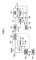
- Fig. 1 is a block diagram of the liquid crystal display device according to the present invention.
- Figs. 8 and 9 show the correction data quantities (addition data quantity and subtraction data quantity) of the liquid crystal of display portions at which the display content changes.
- Fig. 10 is a detailed block diagram of the addition/subtraction data generation circuit shown in Fig. 1.
- Fig. 11 shows the gray-scale voltage level to be applied to the liquid crystals of dispaly portions at which the display content changes.
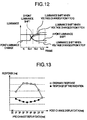
- Fig. 12 shows the change of display luminance relative to the application of the gray-scale voltage shown in Fig. 11.
- Figs. 13 and 14 show the response of the liquid crystal.
- reference numeral 101 denotes a bus for transferring display data and a sync signal inputted from an external device.
- Reference numeral 102 denotes a frame memory control circuit.
- Reference numeral 103 denotes a frame memory control bus.
- Reference numeral 104 denotes a frame memory.
- Reference numeral 105 denotes a data bus for transferring the display data read out from the frame memory 104.
- Reference numeral 106 denotes an addition/subtraction data generation circuit for comparing the display data transferred through the data bus 101 with display data transferred through the data bus 105.
- Reference numeral 107 denotes a data bus for transferring addition/subtraction coefficient data generated by the addition/subtraction coefficient data generation circuit 106.
- Reference numeral 121 denotes a mode signal.
- the mode signal is used for selecting the addition/subtraction coefficient data in accordance with the response characteristics of a liquid crystal material.
- Reference numeral 108 denotes a data addition/subtraction circuit for converting the display data transferred through the data bus 101 on the basis of the addition/subtraction coefficient data 107.
- Reference numeral 109 denotes a bus for transferring a control signal for executing timing control of the display data generated by the addition/subtraction circuit 108, the sync signal, and so forth.
- Reference numeral 110 denotes a timing control circuit for generating various timing signals of the liquid crystal driving circuit.
- Reference numeral 111 denotes a bus for transferring display data and the sync signal generated by the timing control circuit 110.
- Reference numeral 112 denotes a bus for transferring the sync signal generated by the timing control circuit 110 to a scan driving circuit 114.
- Reference numeral 113 denotes a signal driving circuit for generating a gray-scale voltage corresponding to the display data transferred through the bus 111.
- Reference numeral 114 denotes a scan driving circuit for selecting sequentially the lines to which the gray-scale voltages generated by the signal driving circuit 113 are applied.
- Reference numeral 115 denotes a power supply circuit.
- Reference numeral 116 denotes a liquid crystal panel.
- Reference numeral 117 denotes a drain line bus for transferring the gray-scale voltage generated by the signal driving circuit 113 to the liquid crystal panel 116.
- Reference numeral 118 denotes a gate line bus for transferring the scanning voltage generated by the scan driving circuit 114 to the liquid crystal panel 116.
- Reference numeral 119 denotes a power supply bus for transferring a power source voltage to the scanning driving circuit.
- Reference numeral 120 denotes a power supply bus for transferring the power supply voltage to the signal driving circuit 130.
- Reference numeral 121 denotes a mode signal for adjusting an addition data quantity and a subtraction data quantity corresponding to the response of the liquid crystal.
- Reference numeral 122 denotes an integrated circuit block in which the driving circuits for accomplishing high-speed response of the liquid crystal of this embodiment are integrated.
- Fig. 8 shows display data-to-addition data quantity characteristics when the display data changes from dark gray-scale display to bright gray-scale display.
- the abscissa represents post-change display data, and the ordinate represents the addition data quantity for each before-change display data.
- Fig. 9 shows display data-to-subtraction display data quantity characteristics when the display data changes from bright gray-scale display to dark gray-scale display.
- the abscissa represents the post-change display data and the ordinate represents the addition data quantity for each before-change display data.
- the display data is inputed from the external device such as a television tuner or a video recorder (which naturally inputs digital data through the bus 105, when it outputs the analog data, after the analog data is converted to the digital data by a digital data converter), or an information processing unit such as a personal computer.
- the external device such as a television tuner or a video recorder (which naturally inputs digital data through the bus 105, when it outputs the analog data, after the analog data is converted to the digital data by a digital data converter), or an information processing unit such as a personal computer.
- the greater the value of this display data the brighter becomes the pixel. The smaller the value, the darker becomes the pixel.
- Reference numeral 1001 denotes a tilt coefficient generation circuit.
- Reference numeral 1002 denotes an inflection point generation circuit.
- Reference numeral 1003 denotes a data bus for transferring the inflection point data generated by the inflection point generation circuit 1002.
- Reference numeral 1004 denotes an arithmetic operation unit for comparing and computing the display data transferred through the data bus 101 with the display data transferred through the data bus 105.
- Reference numeral 1005 denotes a data bus for transferring the comparison result of the display data transferred through the data bus 105.
- Reference numeral 1006 denotes a data bus for transferring the difference value between the display data transferred through the data bus 101 and the display data transferred through the data bus 105.
- Reference numeral 1007 denotes a data bus for transferring the tilt coefficient data generated by the tilt coefficient generation circuit 1001.
- Reference numeral 1008 denotes an arithmetic operation unit for computing the tilt coefficient data transferred through the data bus 1007 and the difference data transferred through the data bus 1006.
- Fig. 11 shows a gray-scale voltage level to be applied to each liquid crystal at each of the 'A', 'B' and 'C' points for each frame time relative to the change of the display content shown in Fig. 5.
- the display content shown in Fig. 11 are dynamic images at the 'A' and 'C' points and a still image at the 'B' point, for example.
- Fig. 12 corresponds to the change of the display content shown in Fig. 5.
- the abscissa represents the frame time and the ordinate represents display luminance.
- the graph shows a luminance change at each of the 'A', 'B' and 'C' points.
- Fig. 13 the ordinate represents response time of the liquid crystal and the abscissa represents the post-change display data.
- the response of the liquid crystal display device according to the prior art and the response of the liquid crystal display device according to the present invention, when the before-change display data is hex.00, are plotted by circles and dots, respectively in this graph.
- the term "response of liquid crystal” used in this embodiment means the time from the point at which the gray-scale voltage is applied to the pixel of the TFT liquid crystal panel 116 by the signals from the signal driving circuit 113 and the scan driving circuit 114 in Fig. 1 to the point at which the gray-scale voltage so applied is displayed.
- Fig. 14 the ordinate represents the response of the liquid crystal and the abscissa represents the post-change display data in the same way as in Fig. 13.
- the response of the liquid crystal display device according to the prior art and that of the liquid crystal display device according to the present invention are plotted by circles and dots, respectively when the before-change display data is hex.FF.
- the display data and the sync signal inputted from the external device through the bus 101 are stored in the frame memory 104 through the frame memory control circuit 102 and the frame memory control bus 103.
- the frame memory control circuit 102 serially reads out the display data stored in the frame memory 104 after the passage of one frame, and serially outputs them through the data bus 105.
- the frame memory control circuit 102, the frame memory control bus 103 and the frame memory 104 serially repeat this operation.
- the addition/subtraction data generation circuit 106 in the display data inputted to the addition/subtraction data generation circuit 106, becomes the display data that is belated by one frame with respect to the display data transferred through the data bus 105.
- the gray-scale change of the pixels corresponding to two consecutive frames is computed in this way.
- the addition/subtraction data generation circuit 106 can judge whether or not any change exits in the display data between the frames.
- the addition/subtraction data generation circuit 106 can compute the addition/subtraction coefficient data as correction data to be transferred through the data bus from the relationship between the before-change display data and the post-change display data.
- the addition/subtraction coefficient data to be transferred through the data bus 107 have the characteristics shown in Figs. 8 and 9. These characteristics are found out as a result of experiments conducted by the present inventor.
- the form of the addition/subtraction coefficient data shown in Figs. 8 and 9 is different depending on the materials of the liquid crystal panel, and so forth.
- Fig. 8 shows the addition display data quantity characteristics when the display data changes from the dark gray-scale display to the bright gray-scale display. In this graph, the addition display data quantity is increased much more as the difference of the post-change display data from the before-change display data becomes greater, and is decreased when the post-change display data quantity exceeds a certain value.
- the addition data quantity shown in Fig. 8 is the value that takes the normal response time characteristic shown in Fig. 13 into consideration.
- the normal response shown in Fig. 13 is of the black display data of hex.00 as the before-change display data.
- the post-display display data is below intermediate luminance, the response is more likely to become slow when the post-change display data is closer to intermediate luminance.
- the post-change display data exceeds intermediate luminance, the response tends to increase gradually when the post-change display data is closer to the white display. Therefore, when the post-change display data is below intermediate luminance, the addition data quantity is increased much more, and is decreased much more when the post-change display data exceeds intermediate luminance and is closer to the white display. In this way, it becomes possible to achieve the high-rate response optimized for the response characteristics inherent to the liquid crystal.
- a certain inflection point is provided to the liquid crystal having the normal response characteristic shown in Fig. 13.
- the addition data is increased by linear approximation (broken line) till the inflection point with the increase of the post-change display data, and the subtraction data is decreased by linear approximation (broken line) from the inflection point with the decrease of the post-change display data.
- the addition data quantity has an upper limit.
- the difference between the before-change display data and the post-change display data, as represented by the solid line extending from the post-change display data, this upper limit is hex.FF in Fig. 8.
- the addition data takes the upper limit value as its value.
- Fig. 9 shows the subtraction display data quantity characteristics in the case where the display data changes from the bright gray-scale display to the dark gray-scale display.
- the addition display data quantity is increased much more as the difference of the post-change display data from the before-change display data becomes greater.
- the subtraction data quantity shown in Fig. 9 has the value that takes the normal response time shown in Fig. 14 into consideration.
- the before-change display data is the white display data of hex.FF.
- the normal response time shown in Fig. 14 has the characteristic such that the closer the post-change display data to intermediate luminance, the slower becomes the response.
- the normal response time has the characteristic such that the closer the post-change display data to the black display, the higher becomes gradually the response. Therefore, when the post-change display data is below intermediate luminance, the subtraction data quantity is increased much more when the post-change display data is closer to intermediate luminance.
- the subtraction data quantity is decreased. In this way, high response, that takes the response characteristics inherent to the liquid crystal into consideration, can be accomplished.
- the inflection point is the upper limit value of the subtraction data quantity (that is, the difference between the before-change display data and the post-change display data as represented by the solid line extending from hex.00 of the post-change display data shown in Fig. 8).
- the subtraction data is increased by linear approximation (broken line) till the subtraction data reaches the upper limit, and uses the upper limit value as the subtraction data quantity after the subtraction data quantity reaches the upper limit value.
- the addition data and the subtraction data can be optimized by providing the inflection point in consideration of the response characteristic from the before-change display data to the post-change display data and by executing linear approximation with the increase of the post-change display data.
- a tilt coefficient generation circuit 1001 generates tilt coefficient data from the display data, that is the display data of one preceding frame, transferred through the data bus 105.
- This tilt coefficient is for computing the addition/subtraction data quantity corresponding to the post-change display data plotted in Fig. 8, and represents the tilt indicated by broken line.
- the post-change display data are below hex.7F and above hex.7F.
- An inflection point generation circuit 1002 generates this hex.7F as the inflection point and inputs it to the tilt coefficient generation circuit 1001 through the data bus 1003.
- Another example of the kind of the tilt is the difference between Fig. 8 and Fig. 9.
- the tilt coefficient generation circuit 1001 it is the difference between the case where the before-change display data is greater than the post-change display data and the case where the former is smaller than the latter.
- the tilt coefficient becomes different in such a case, too.
- An arithmetic unit 1004 generates this difference, and inputs it to the tilt coefficient generation circuit 1001 through the data bus 1005. Furthermore, the response changes depending on the characteristics of the liquid crystal materials, and a mode signal 121 is inputted therefore to the tilt coefficient generation circuit 1001.
- the circuit of the tilt coefficient generation circuit 1001 may be modified in accordance with the characteristics of the liquid crystal without disposing this mode signal 121.
- the tilt coefficient generation circuit 1001 transfers the tilt coefficient data to the arithmetic operation unit 1008 through the data bus 1007, and the arithmetic operation unit detects the portion at which the display data changes. In this way, the addition/subtraction coefficient data as the correction data can be generated.
- the difference data transferred through the data bus 1006 becomes '0'. Therefore, the addition/subtraction coefficient data transferred through the data bus 107, too, becomes '0'. Needless to say, the correction data is not added to, or subtracted from, the display data in this case.
- the addition/subtraction data generated by the addition/subtraction data generation circuit 106 is inputted to the data addition circuit 108 through the data bus 107.
- the data addition/subtraction circuit 108 can add or subtract the correction data to or from the portion at which the display content changes.
- the addition/subtraction data generation circuit 106 and the data addition/subtraction circuit 108 are described separately.
- the addition/subtraction data generation circuit 106 is the circuit that must be optimized in accordance with the characteristics of the liquid crystal.
- this addition/subtraction data is obtained by linear approximation.
- subtraction data is obtained by linear approximation.
- similar effects can be obtained also by means that stores in advance the addition coefficient data quantity and the subtraction coefficient data quantity obtained from the before-change display data and the post-change display data in a memory circuit, as described already.
- the signal driving circuit 113 converts the display data transferred thereto through the data bus 111 to the corresponding gray-scale voltage and outputs it to the drain line bus 117.
- the signal driving circuit 113 executes the operation of converting this display data to the gray-scale voltage simultaneously for all the pixels of one horizontal line.
- the scan driving circuit 114 sets the line, to which the gray-scale voltage is applied, to the selection state in synchronism with the timing at which the signal driving circuit 113 outputs the gray-scale voltage to the drain line bus 117.
- This operation is carried out sequentially for each line, so that the gray-scale voltages corresponding to the display data for one screen can be applied to each pixel portion and furthermore, display luminance corresponding to the display data can be obtained.
- Fig. 5 showing the prior art example, the square is displayed in the display region including the 'A' and 'B' points at the time of the N frame, and the background is displayed at the 'C' point.
- This square moves to a region inclusive of the 'B' and 'C" points at the time of the (N+1) frame.
- the display content changes from the square display to the background display at the 'A' point, remains unchanged at the 'B' point and changes from the background display to the square display at the 'C' point.
- the gray-scale voltage applied to the liquid crystal of each pixel portion changes with the change of this display content.
- the voltage X is applied at the 'A' point in the N frame.
- the correction data is subtracted from the original display data in the (N+1) frame because the display content changes, and the voltage P is applied. Since the display content is coincident with that of the (N+1) frame in the (N+2) frame and so on, the voltage Y that is the gray-scale voltage corresponding to the original display data is applied.
- Fig. 12 shows the luminance shift state representing the response of the liquid crystal from this voltage applied state.
- the luminance change at the 'A' point changes in the (N+1) frame with the luminance shift in which the voltage changes from the voltage X to the voltage P.
- the original voltage Y is applied in the (N+2) frame and so on.
- the response of the liquid crystal can be speeded up much more than when the gray-scale voltage corresponding to the display data is applied as in the prior art.
- this embodiment describes the addition/subtraction data generation circuit 106, the data addition/subtraction circuit 108.
- the frame memories 104 and the timing control circuit 110 may be integrated in the same chip as needed.
- the embodiment of the present invention can speed up the response of the liquid crystal without changing the characteristics of the liquid crystal materials as shown in Figs. 13 and 14. Since the content displayed in the preceding frame is not displayed as the after-image, this embodiment provides the effect that high image quality display becomes possible. The embodiment provides greater effects particularly for the display of dynamic images in the televisions using very often the intermediate luminance display.
- the interface portion of the liquid crystal display device is the same as that of the liquid crystal display device of the prior art.
- the present invention can be applied easily to existing systems and can accomplish the liquid crystal display device at a low cost of production.
Landscapes
- Engineering & Computer Science (AREA)
- Chemical & Material Sciences (AREA)
- Crystallography & Structural Chemistry (AREA)
- Physics & Mathematics (AREA)
- Computer Hardware Design (AREA)
- General Physics & Mathematics (AREA)
- Theoretical Computer Science (AREA)
- Control Of Indicators Other Than Cathode Ray Tubes (AREA)
- Liquid Crystal Display Device Control (AREA)
- Liquid Crystal (AREA)
Applications Claiming Priority (2)
| Application Number | Priority Date | Filing Date | Title |
|---|---|---|---|
| JP29488199A JP2001117074A (ja) | 1999-10-18 | 1999-10-18 | 液晶表示装置 |
| JP29488199 | 1999-10-18 |
Publications (3)
| Publication Number | Publication Date |
|---|---|
| EP1094437A2 true EP1094437A2 (fr) | 2001-04-25 |
| EP1094437A3 EP1094437A3 (fr) | 2003-01-02 |
| EP1094437B1 EP1094437B1 (fr) | 2010-05-05 |
Family
ID=17813467
Family Applications (1)
| Application Number | Title | Priority Date | Filing Date |
|---|---|---|---|
| EP00119134A Expired - Lifetime EP1094437B1 (fr) | 1999-10-18 | 2000-09-04 | Dispositif d'affichage à cristaux liquides doté de caractéristiques améliorées de réponse |
Country Status (6)
| Country | Link |
|---|---|
| US (3) | US6556180B1 (fr) |
| EP (1) | EP1094437B1 (fr) |
| JP (1) | JP2001117074A (fr) |
| KR (1) | KR100363350B1 (fr) |
| DE (1) | DE60044327D1 (fr) |
| TW (1) | TW493147B (fr) |
Cited By (1)
| Publication number | Priority date | Publication date | Assignee | Title |
|---|---|---|---|---|
| EP2241861A4 (fr) * | 2008-01-22 | 2013-02-27 | Sharp Kk | Système d'affichage, dispositif de commande d'affichage, dispositif d'affichage d'image |
Families Citing this family (63)
| Publication number | Priority date | Publication date | Assignee | Title |
|---|---|---|---|---|
| TW513598B (en) * | 2000-03-29 | 2002-12-11 | Sharp Kk | Liquid crystal display device |
| JP3769463B2 (ja) * | 2000-07-06 | 2006-04-26 | 株式会社日立製作所 | 表示装置、表示装置を備えた画像再生装置及びその駆動方法 |
| JP3722677B2 (ja) * | 2000-08-18 | 2005-11-30 | 株式会社アドバンスト・ディスプレイ | 液晶表示装置 |
| JP2002099249A (ja) * | 2000-09-21 | 2002-04-05 | Advanced Display Inc | 表示装置および表示装置の駆動方法 |
| JP3520863B2 (ja) * | 2000-10-04 | 2004-04-19 | セイコーエプソン株式会社 | 画像信号補正回路、その補正方法、液晶表示装置及び電子機器 |
| JP2002123213A (ja) * | 2000-10-18 | 2002-04-26 | Fujitsu Ltd | 画像表示のためのデータ変換方法 |
| JP2002158893A (ja) * | 2000-11-22 | 2002-05-31 | Minolta Co Ltd | 画像補正装置、画像補正方法および記録媒体 |
| KR100363540B1 (ko) * | 2000-12-21 | 2002-12-05 | 삼성전자 주식회사 | 고속으로 구동되는 액정 디스플레이 장치 및 그것을 위한계조전압 발생회로 |
| KR100381963B1 (ko) * | 2000-12-26 | 2003-04-26 | 삼성전자주식회사 | 감소된 플리커를 갖는 액정 표시 장치 및 그것의 플리커저감 방법 |
| JP4599743B2 (ja) * | 2001-03-30 | 2010-12-15 | 日本電気株式会社 | ホールド型表示素子、ディスプレイ、モニタ、ライトバルブ及びプロジェクタ |
| JP3614792B2 (ja) * | 2001-04-23 | 2005-01-26 | ウインテスト株式会社 | アクティブマトリックス型ディスプレイの画素検査装置および画素検査方法 |
| KR100796748B1 (ko) * | 2001-05-11 | 2008-01-22 | 삼성전자주식회사 | 액정 표시 장치와 이의 구동 장치 |
| KR100421500B1 (ko) * | 2001-06-09 | 2004-03-12 | 엘지.필립스 엘시디 주식회사 | 액정표시장치의 색보정 방법 및 장치 |
| JP2003005154A (ja) * | 2001-06-20 | 2003-01-08 | Toshiba Corp | 液晶表示装置の制御装置 |
| JP2003044017A (ja) * | 2001-08-03 | 2003-02-14 | Nec Corp | 画像表示装置 |
| KR100806901B1 (ko) * | 2001-09-03 | 2008-02-22 | 삼성전자주식회사 | 광시야각 모드용 액정 표시 장치와 이의 구동 방법 |
| KR20030027202A (ko) * | 2001-09-14 | 2003-04-07 | 비오이 하이디스 테크놀로지 주식회사 | 액정표시장치의 고속응답 구동방법 |
| KR100431000B1 (ko) * | 2001-10-23 | 2004-05-12 | 삼성전자주식회사 | 영상블록화현상 보상장치 및 방법 |
| KR100438827B1 (ko) * | 2001-10-31 | 2004-07-05 | 삼성전기주식회사 | 영상의 계조 향상 방법 및 이를 수행하는 영상 표시 장치 |
| KR100840316B1 (ko) * | 2001-11-26 | 2008-06-20 | 삼성전자주식회사 | 액정 표시 장치 및 그의 구동 방법 |
| JP3749473B2 (ja) * | 2001-11-29 | 2006-03-01 | 株式会社日立製作所 | 表示装置 |
| JP3642328B2 (ja) * | 2001-12-05 | 2005-04-27 | セイコーエプソン株式会社 | 電気光学装置、その駆動回路、駆動方法及び電子機器 |
| JP2003241721A (ja) * | 2002-02-20 | 2003-08-29 | Fujitsu Display Technologies Corp | 液晶パネルの表示制御装置および液晶表示装置 |
| KR100853210B1 (ko) * | 2002-03-21 | 2008-08-20 | 삼성전자주식회사 | 색 특성 보상 기능과 응답 속도 보상 기능을 갖는 액정표시 장치 |
| KR100477643B1 (ko) * | 2002-04-10 | 2005-03-23 | 삼성전자주식회사 | 응답 속도 개선 장치 및 방법 |
| KR100825103B1 (ko) | 2002-05-16 | 2008-04-25 | 삼성전자주식회사 | 액정 표시 장치 및 그 구동 방법 |
| JP3818649B2 (ja) * | 2002-05-20 | 2006-09-06 | インターナショナル・ビジネス・マシーンズ・コーポレーション | 画像表示システム、画像表示方法、およびプログラム |
| JP3710131B2 (ja) * | 2002-05-29 | 2005-10-26 | シャープ株式会社 | 画像処理装置および画像処理方法、並びに画像表示装置、携帯電子機器 |
| KR100898783B1 (ko) * | 2002-09-19 | 2009-05-20 | 엘지디스플레이 주식회사 | 액정표시장치 및 그 구동방법 |
| KR100493031B1 (ko) * | 2002-11-08 | 2005-06-07 | 삼성전자주식회사 | 액정 표시 장치를 구동하는 반응 시간 가속 장치 및 그 방법 |
| KR100908655B1 (ko) * | 2002-11-27 | 2009-07-21 | 엘지디스플레이 주식회사 | 데이터 공급시간의 변조방법과 이를 이용한액정표시장치의 구동방법 및 장치 |
| KR100915234B1 (ko) * | 2002-12-17 | 2009-09-02 | 삼성전자주식회사 | 계조 전압의 선택 범위를 변경할 수 있는 액정 표시장치의 구동 장치 및 그 방법 |
| JP2004271609A (ja) * | 2003-03-05 | 2004-09-30 | Canon Inc | 表示装置の駆動方法 |
| US7142186B2 (en) * | 2003-03-24 | 2006-11-28 | Hivix Co., Ltd | Method and apparatus for converting gradation data in STN LCD |
| TWI251199B (en) * | 2003-03-31 | 2006-03-11 | Sharp Kk | Image processing method and liquid-crystal display device using the same |
| JP2007503614A (ja) * | 2003-08-22 | 2007-02-22 | コーニンクレッカ フィリップス エレクトロニクス エヌ ヴィ | イナーシャプローン画像表示装置を駆動するためのシステム |
| US7362290B2 (en) | 2003-10-29 | 2008-04-22 | Seiko Epson Corporation | Image signal correcting circuit, image processing method, electro-optical device and electronic apparatus |
| US8493298B2 (en) * | 2003-11-01 | 2013-07-23 | Silicon Quest Kabushiki-Kaisha | Video display system |
| JP2005202159A (ja) | 2004-01-15 | 2005-07-28 | Seiko Epson Corp | 電気光学装置、その駆動回路、その駆動方法および電子機器 |
| JP4201338B2 (ja) * | 2004-02-03 | 2008-12-24 | シャープ株式会社 | 画像処理装置、画像処理方法、画像表示装置、携帯用情報機器、制御プログラムおよび可読記録媒体 |
| JP2005257854A (ja) * | 2004-03-10 | 2005-09-22 | Nec Electronics Corp | 表示装置用駆動回路、表示装置の駆動方法及び表示装置 |
| JP2005316146A (ja) * | 2004-04-28 | 2005-11-10 | Fujitsu Display Technologies Corp | 液晶表示装置及びその処理方法 |
| JP4413730B2 (ja) | 2004-09-28 | 2010-02-10 | 富士通株式会社 | 液晶表示装置及びその駆動方法 |
| KR100685820B1 (ko) * | 2005-02-22 | 2007-02-22 | 삼성에스디아이 주식회사 | 전향경로 회로부가 구비되는 액정표시장치 |
| WO2006095460A1 (fr) * | 2005-03-10 | 2006-09-14 | Mitsubishi Denki Kabushiki Kaisha | Dispositif et procede de traitement d'image et dispositif d'affichage d'image |
| KR100731048B1 (ko) * | 2005-10-20 | 2007-06-22 | 엘지.필립스 엘시디 주식회사 | 액정 표시장치의 구동장치 및 구동방법 |
| TWI319170B (en) * | 2005-11-11 | 2010-01-01 | Au Optronics Corp | Lcd display method and a system thereof |
| JP4839083B2 (ja) | 2005-12-27 | 2011-12-14 | 矢崎総業株式会社 | 液晶表示メータ |
| CN100446081C (zh) * | 2006-06-07 | 2008-12-24 | 友达光电股份有限公司 | 液晶显示面板及其时序控制器与过驱动参数的产生方法 |
| KR101252879B1 (ko) * | 2006-06-29 | 2013-04-09 | 엘지디스플레이 주식회사 | 액정표시장치 및 그의 구동방법 |
| US7674662B2 (en) | 2006-07-19 | 2010-03-09 | Applied Materials, Inc. | Process for making thin film field effect transistors using zinc oxide |
| JP2008064841A (ja) * | 2006-09-05 | 2008-03-21 | Renesas Technology Corp | 表示制御装置、半導体集積回路及び携帯端末システム |
| JP2008070715A (ja) * | 2006-09-15 | 2008-03-27 | Renesas Technology Corp | 半導体集積回路及び携帯端末システム |
| JP5229713B2 (ja) * | 2007-01-29 | 2013-07-03 | 株式会社ジャパンディスプレイイースト | 表示装置 |
| KR100800493B1 (ko) * | 2007-02-09 | 2008-02-04 | 삼성전자주식회사 | 임베디드 메모리 장치를 이용한 액정 표시 장치의 응답속도 보상 시스템 및 영상 프레임 데이터 제어 방법 |
| US8115785B2 (en) * | 2007-04-26 | 2012-02-14 | Semiconductor Energy Laboratory Co., Ltd. | Method for driving liquid crystal display device, liquid crystal display device, and electronic device |
| US7927713B2 (en) | 2007-04-27 | 2011-04-19 | Applied Materials, Inc. | Thin film semiconductor material produced through reactive sputtering of zinc target using nitrogen gases |
| JP5050691B2 (ja) * | 2007-07-05 | 2012-10-17 | ソニー株式会社 | 画像処理装置、画像処理方法およびコンピュータプログラム |
| TWI372377B (en) * | 2007-11-21 | 2012-09-11 | Mstar Semiconductor Inc | Method and apparatus for eliminating image blur by pixel-based processing |
| KR100927210B1 (ko) * | 2007-12-27 | 2009-11-16 | 한국과학기술원 | 전자종이 표시장치의 차등적 프레임 입력 방법 |
| US9615213B2 (en) * | 2009-07-21 | 2017-04-04 | Katasi Llc | Method and system for controlling and modifying driving behaviors |
| WO2011092919A1 (fr) * | 2010-01-28 | 2011-08-04 | シャープ株式会社 | Dispositif d'affichage à cristaux liquides, procédé d'affichage, programme et support d'enregistrement |
| WO2018078748A1 (fr) * | 2016-10-26 | 2018-05-03 | 堺ディスプレイプロダクト株式会社 | Dispositif d'affichage à cristaux liquides et procédé de pilotage de dispositif d'affichage à cristaux liquides |
Family Cites Families (35)
| Publication number | Priority date | Publication date | Assignee | Title |
|---|---|---|---|---|
| JP2708746B2 (ja) | 1987-07-03 | 1998-02-04 | 三菱電機株式会社 | 液晶制御回路 |
| JP2523358B2 (ja) | 1988-10-21 | 1996-08-07 | 株式会社ワイ・イー・データ | 磁気デイスク駆動装置に於けるシ―ク動作制御方式 |
| JPH02113294A (ja) | 1988-10-24 | 1990-04-25 | Toshiba Corp | 液晶表示装置 |
| JPH0363692A (ja) | 1989-08-01 | 1991-03-19 | Sharp Corp | 表示装置の駆動回路 |
| JP2650479B2 (ja) | 1989-09-05 | 1997-09-03 | 松下電器産業株式会社 | 液晶制御回路および液晶パネルの駆動方法 |
| JPH0396696U (fr) | 1990-01-19 | 1991-10-03 | ||
| US5828354A (en) * | 1990-07-13 | 1998-10-27 | Citizen Watch Co., Ltd. | Electrooptical display device |
| JP3167351B2 (ja) | 1990-09-03 | 2001-05-21 | 株式会社東芝 | 液晶表示装置 |
| NL9002516A (nl) * | 1990-11-19 | 1992-06-16 | Philips Nv | Weergeefinrichting en werkwijze ter vervaardiging daarvan. |
| US5347294A (en) * | 1991-04-17 | 1994-09-13 | Casio Computer Co., Ltd. | Image display apparatus |
| JPH04365094A (ja) | 1991-06-12 | 1992-12-17 | Casio Comput Co Ltd | 液晶表示装置 |
| JP3052418B2 (ja) | 1991-04-17 | 2000-06-12 | カシオ計算機株式会社 | 液晶パネル駆動装置 |
| JP3349527B2 (ja) * | 1991-10-01 | 2002-11-25 | 株式会社日立製作所 | 液晶中間調表示装置 |
| GB9218754D0 (en) | 1992-09-04 | 1992-10-21 | Univ London | Device for use in securing a thread |
| JP3288142B2 (ja) * | 1992-10-20 | 2002-06-04 | 富士通株式会社 | 液晶表示装置およびその駆動方法 |
| JP3331687B2 (ja) | 1993-08-10 | 2002-10-07 | カシオ計算機株式会社 | 液晶パネル駆動装置 |
| JPH07121143A (ja) | 1993-10-20 | 1995-05-12 | Casio Comput Co Ltd | 液晶表示装置及び液晶駆動方法 |
| JP3396929B2 (ja) | 1993-11-02 | 2003-04-14 | カシオ計算機株式会社 | 画像表示装置 |
| CA2138834C (fr) * | 1994-01-07 | 2004-10-19 | Robert J. Gove | Systeme d'affichage video a desentrelacement numerique |
| JP3511409B2 (ja) * | 1994-10-27 | 2004-03-29 | 株式会社半導体エネルギー研究所 | アクティブマトリクス型液晶表示装置およびその駆動方法 |
| US6100859A (en) * | 1995-09-01 | 2000-08-08 | Fujitsu Limited | Panel display adjusting number of sustaining discharge pulses according to the quantity of display data |
| JPH0981083A (ja) | 1995-09-13 | 1997-03-28 | Toshiba Corp | 表示装置 |
| JPH09138666A (ja) * | 1995-11-10 | 1997-05-27 | Fujitsu General Ltd | 表示装置の動画補正方法及び動画補正装置 |
| JPH1039837A (ja) | 1996-07-22 | 1998-02-13 | Hitachi Ltd | 液晶表示装置 |
| JP3712802B2 (ja) * | 1996-10-29 | 2005-11-02 | 富士通株式会社 | 中間調表示方法および表示装置 |
| JP3349638B2 (ja) * | 1996-11-15 | 2002-11-25 | シャープ株式会社 | 表示装置を駆動する方法および回路 |
| JPH10161587A (ja) | 1996-11-29 | 1998-06-19 | Fujitsu General Ltd | 表示装置の動画補正方法及び動画補正回路 |
| US6353435B2 (en) * | 1997-04-15 | 2002-03-05 | Hitachi, Ltd | Liquid crystal display control apparatus and liquid crystal display apparatus |
| JP2001500994A (ja) * | 1997-07-22 | 2001-01-23 | コーニンクレッカ フィリップス エレクトロニクス エヌ ヴィ | 表示装置 |
| KR100237685B1 (ko) * | 1997-09-09 | 2000-01-15 | 윤종용 | 전력 제어 회로를 갖는 액정 표시 장치 |
| JP3305240B2 (ja) | 1997-10-23 | 2002-07-22 | キヤノン株式会社 | 液晶表示パネル駆動装置と駆動方法 |
| TW490580B (en) * | 1998-11-13 | 2002-06-11 | Hitachi Ltd | Liquid crystal display apparatus and its drive method |
| JP3840027B2 (ja) * | 1999-02-26 | 2006-11-01 | キヤノン株式会社 | 画像表示装置及び表示制御方法 |
| JP3944394B2 (ja) * | 2002-01-08 | 2007-07-11 | 株式会社日立製作所 | 表示装置 |
| JP4074207B2 (ja) * | 2003-03-10 | 2008-04-09 | 株式会社 日立ディスプレイズ | 液晶表示装置 |
-
1999
- 1999-10-18 JP JP29488199A patent/JP2001117074A/ja active Pending
-
2000
- 2000-09-04 TW TW089118060A patent/TW493147B/zh not_active IP Right Cessation
- 2000-09-04 DE DE60044327T patent/DE60044327D1/de not_active Expired - Lifetime
- 2000-09-04 EP EP00119134A patent/EP1094437B1/fr not_active Expired - Lifetime
- 2000-09-06 US US09/655,826 patent/US6556180B1/en not_active Expired - Lifetime
- 2000-09-19 KR KR1020000054835A patent/KR100363350B1/ko not_active Expired - Fee Related
-
2003
- 2003-02-11 US US10/361,647 patent/US6714181B2/en not_active Expired - Lifetime
-
2004
- 2004-01-14 US US10/756,510 patent/US7061511B2/en not_active Expired - Fee Related
Cited By (1)
| Publication number | Priority date | Publication date | Assignee | Title |
|---|---|---|---|---|
| EP2241861A4 (fr) * | 2008-01-22 | 2013-02-27 | Sharp Kk | Système d'affichage, dispositif de commande d'affichage, dispositif d'affichage d'image |
Also Published As
| Publication number | Publication date |
|---|---|
| US6556180B1 (en) | 2003-04-29 |
| KR20010050512A (ko) | 2001-06-15 |
| DE60044327D1 (de) | 2010-06-17 |
| US20050062701A1 (en) | 2005-03-24 |
| TW493147B (en) | 2002-07-01 |
| JP2001117074A (ja) | 2001-04-27 |
| EP1094437B1 (fr) | 2010-05-05 |
| US7061511B2 (en) | 2006-06-13 |
| EP1094437A3 (fr) | 2003-01-02 |
| US6714181B2 (en) | 2004-03-30 |
| KR100363350B1 (ko) | 2002-12-05 |
| US20030117358A1 (en) | 2003-06-26 |
Similar Documents
| Publication | Publication Date | Title |
|---|---|---|
| US6556180B1 (en) | Liquid crystal display device having improved-response-characteristic drivability | |
| US7450104B2 (en) | Method and apparatus for driving liquid crystal display | |
| US7847782B2 (en) | Method and apparatus for driving liquid crystal display | |
| US7466301B2 (en) | Method of driving a display adaptive for making a stable brightness of a back light unit | |
| US8462091B2 (en) | Method for driving liquid crystal display apparatus | |
| KR100485557B1 (ko) | 표시 장치 | |
| JP4679066B2 (ja) | 表示装置及び駆動方法 | |
| US7847771B2 (en) | Display device capable of adjusting divided data in one frame | |
| EP0911795A2 (fr) | Methode et dispositif de commande d'un panneau d'affichage à cristaux liquides | |
| KR101051895B1 (ko) | 디스플레이 디바이스, 디스플레이 패널 드라이버, 디스플레이 패널 구동 방법, 및 이미지 데이터를 디스플레이 패널 드라이버에 제공하는 방법 | |
| US20020030652A1 (en) | Liquid crystal display device and drive circuit device for | |
| US20100302287A1 (en) | Display driving device and display driving system | |
| KR20070059077A (ko) | 액정 셀의 모션 블러 감소 방법 및 시스템, 컴퓨터프로그램 | |
| US20080158212A1 (en) | Display Device and Display System | |
| KR20020070962A (ko) | 오씨비 셀을 이용한 액정 표시장치 및 그 구동방법 | |
| US5739808A (en) | Display control method and apparatus | |
| US10235971B1 (en) | System and method for enhancing display uniformity at display boundaries | |
| US8260077B2 (en) | Method and apparatus for eliminating image blur | |
| KR100545401B1 (ko) | 평판 디스플레이의 화질 조정 장치 및 그 방법 | |
| EP1903545A2 (fr) | Dispositif d'affichage | |
| KR101399237B1 (ko) | 액정표시장치 및 그의 구동방법 | |
| KR100926306B1 (ko) | 액정 표시 장치와 이의 구동 장치 및 방법 | |
| KR101616924B1 (ko) | 액정표시장치 | |
| KR20030065816A (ko) | 박막트랜지스터 액정표시장치의 고속 응답을 위한 구동 회로 | |
| Lee et al. | 60.3: Spatio‐Temporal Edge Enhancement for Reducing Motion Blur |
Legal Events
| Date | Code | Title | Description |
|---|---|---|---|
| PUAI | Public reference made under article 153(3) epc to a published international application that has entered the european phase |
Free format text: ORIGINAL CODE: 0009012 |
|
| AK | Designated contracting states |
Kind code of ref document: A2 Designated state(s): AT BE CH CY DE DK ES FI FR GB GR IE IT LI LU MC NL PT SE |
|
| AX | Request for extension of the european patent |
Free format text: AL;LT;LV;MK;RO;SI |
|
| PUAL | Search report despatched |
Free format text: ORIGINAL CODE: 0009013 |
|
| AK | Designated contracting states |
Kind code of ref document: A3 Designated state(s): AT BE CH CY DE DK ES FI FR GB GR IE IT LI LU MC NL PT SE |
|
| AX | Request for extension of the european patent |
Free format text: AL;LT;LV;MK;RO;SI |
|
| 17P | Request for examination filed |
Effective date: 20030130 |
|
| 17Q | First examination report despatched |
Effective date: 20030515 |
|
| AKX | Designation fees paid |
Designated state(s): DE FR GB NL |
|
| GRAJ | Information related to disapproval of communication of intention to grant by the applicant or resumption of examination proceedings by the epo deleted |
Free format text: ORIGINAL CODE: EPIDOSDIGR1 |
|
| GRAP | Despatch of communication of intention to grant a patent |
Free format text: ORIGINAL CODE: EPIDOSNIGR1 |
|
| GRAS | Grant fee paid |
Free format text: ORIGINAL CODE: EPIDOSNIGR3 |
|
| GRAA | (expected) grant |
Free format text: ORIGINAL CODE: 0009210 |
|
| AK | Designated contracting states |
Kind code of ref document: B1 Designated state(s): DE FR GB NL |
|
| REG | Reference to a national code |
Ref country code: GB Ref legal event code: FG4D |
|
| REF | Corresponds to: |
Ref document number: 60044327 Country of ref document: DE Date of ref document: 20100617 Kind code of ref document: P |
|
| REG | Reference to a national code |
Ref country code: NL Ref legal event code: VDEP Effective date: 20100505 |
|
| PG25 | Lapsed in a contracting state [announced via postgrant information from national office to epo] |
Ref country code: NL Free format text: LAPSE BECAUSE OF FAILURE TO SUBMIT A TRANSLATION OF THE DESCRIPTION OR TO PAY THE FEE WITHIN THE PRESCRIBED TIME-LIMIT Effective date: 20100505 |
|
| PLBE | No opposition filed within time limit |
Free format text: ORIGINAL CODE: 0009261 |
|
| STAA | Information on the status of an ep patent application or granted ep patent |
Free format text: STATUS: NO OPPOSITION FILED WITHIN TIME LIMIT |
|
| 26N | No opposition filed |
Effective date: 20110208 |
|
| REG | Reference to a national code |
Ref country code: GB Ref legal event code: 732E Free format text: REGISTERED BETWEEN 20110428 AND 20110504 |
|
| REG | Reference to a national code |
Ref country code: DE Ref legal event code: R097 Ref document number: 60044327 Country of ref document: DE Effective date: 20110207 |
|
| REG | Reference to a national code |
Ref country code: FR Ref legal event code: ST Effective date: 20110531 |
|
| REG | Reference to a national code |
Ref country code: DE Ref legal event code: R081 Ref document number: 60044327 Country of ref document: DE Owner name: PANASONIC LIQUID CRYSTAL DISPLAY CO., LTD., HI, JP Free format text: FORMER OWNER: HITACHI, LTD., HITACHI VIDEO & INFORMATION SYS, , JP Effective date: 20110506 Ref country code: DE Ref legal event code: R081 Ref document number: 60044327 Country of ref document: DE Owner name: HITACHI DISPLAYS, LTD., MOBARA, JP Free format text: FORMER OWNER: HITACHI, LTD., HITACHI VIDEO & INFORMATION SYS, , JP Effective date: 20110506 Ref country code: DE Ref legal event code: R081 Ref document number: 60044327 Country of ref document: DE Owner name: PANASONIC LIQUID CRYSTAL DISPLAY CO., LTD., HI, JP Free format text: FORMER OWNERS: HITACHI, LTD., TOKYO, JP; HITACHI VIDEO & INFORMATION SYSTEM, INC., YOKOHAMA, KANAGAWA, JP Effective date: 20110506 Ref country code: DE Ref legal event code: R081 Ref document number: 60044327 Country of ref document: DE Owner name: HITACHI DISPLAYS, LTD., MOBARA, JP Free format text: FORMER OWNERS: HITACHI, LTD., TOKYO, JP; HITACHI VIDEO & INFORMATION SYSTEM, INC., YOKOHAMA, KANAGAWA, JP Effective date: 20110506 |
|
| PG25 | Lapsed in a contracting state [announced via postgrant information from national office to epo] |
Ref country code: FR Free format text: LAPSE BECAUSE OF NON-PAYMENT OF DUE FEES Effective date: 20100930 |
|
| REG | Reference to a national code |
Ref country code: GB Ref legal event code: 732E Free format text: REGISTERED BETWEEN 20111103 AND 20111109 |
|
| REG | Reference to a national code |
Ref country code: GB Ref legal event code: 732E Free format text: REGISTERED BETWEEN 20120112 AND 20120118 Ref country code: DE Ref legal event code: R082 Ref document number: 60044327 Country of ref document: DE Representative=s name: STREHL, SCHUEBEL-HOPF & PARTNER, DE |
|
| REG | Reference to a national code |
Ref country code: DE Ref legal event code: R081 Ref document number: 60044327 Country of ref document: DE Owner name: PANASONIC LIQUID CRYSTAL DISPLAY CO., LTD., HI, JP Free format text: FORMER OWNER: HITACHI DISPLAYS, LTD., MOBARA, CHIBA, JP Effective date: 20120208 Ref country code: DE Ref legal event code: R082 Ref document number: 60044327 Country of ref document: DE Representative=s name: STREHL SCHUEBEL-HOPF & PARTNER MBB PATENTANWAE, DE Effective date: 20120208 Ref country code: DE Ref legal event code: R081 Ref document number: 60044327 Country of ref document: DE Owner name: HITACHI DISPLAYS, LTD., MOBARA, JP Free format text: FORMER OWNER: HITACHI DISPLAYS, LTD., MOBARA, CHIBA, JP Effective date: 20120208 Ref country code: DE Ref legal event code: R082 Ref document number: 60044327 Country of ref document: DE Representative=s name: PATENTANWAELTE STREHL, SCHUEBEL-HOPF & PARTNER, DE Effective date: 20120208 |
|
| REG | Reference to a national code |
Ref country code: GB Ref legal event code: 732E Free format text: REGISTERED BETWEEN 20120510 AND 20120516 |
|
| REG | Reference to a national code |
Ref country code: GB Ref legal event code: 732E Free format text: REGISTERED BETWEEN 20120517 AND 20120523 |
|
| PGFP | Annual fee paid to national office [announced via postgrant information from national office to epo] |
Ref country code: DE Payment date: 20170830 Year of fee payment: 18 |
|
| PGFP | Annual fee paid to national office [announced via postgrant information from national office to epo] |
Ref country code: GB Payment date: 20180829 Year of fee payment: 19 |
|
| REG | Reference to a national code |
Ref country code: DE Ref legal event code: R119 Ref document number: 60044327 Country of ref document: DE |
|
| PG25 | Lapsed in a contracting state [announced via postgrant information from national office to epo] |
Ref country code: DE Free format text: LAPSE BECAUSE OF NON-PAYMENT OF DUE FEES Effective date: 20190402 |
|
| GBPC | Gb: european patent ceased through non-payment of renewal fee |
Effective date: 20190904 |
|
| PG25 | Lapsed in a contracting state [announced via postgrant information from national office to epo] |
Ref country code: GB Free format text: LAPSE BECAUSE OF NON-PAYMENT OF DUE FEES Effective date: 20190904 |