EP1094477B1 - Composition dielectrique céramique et composant électronique - Google Patents
Composition dielectrique céramique et composant électronique Download PDFInfo
- Publication number
- EP1094477B1 EP1094477B1 EP00122255A EP00122255A EP1094477B1 EP 1094477 B1 EP1094477 B1 EP 1094477B1 EP 00122255 A EP00122255 A EP 00122255A EP 00122255 A EP00122255 A EP 00122255A EP 1094477 B1 EP1094477 B1 EP 1094477B1
- Authority
- EP
- European Patent Office
- Prior art keywords
- subcomponent
- moles
- temperature
- peak
- dielectric ceramic
- Prior art date
- Legal status (The legal status is an assumption and is not a legal conclusion. Google has not performed a legal analysis and makes no representation as to the accuracy of the status listed.)
- Expired - Lifetime
Links
- 239000000203 mixture Substances 0.000 title claims description 102
- 239000000919 ceramic Substances 0.000 title claims description 64
- 229910002113 barium titanate Inorganic materials 0.000 claims description 36
- 239000003990 capacitor Substances 0.000 claims description 36
- 229910002976 CaZrO3 Inorganic materials 0.000 claims description 30
- 238000000034 method Methods 0.000 claims description 29
- 239000013078 crystal Substances 0.000 claims description 18
- VYPSYNLAJGMNEJ-UHFFFAOYSA-N Silicium dioxide Chemical compound O=[Si]=O VYPSYNLAJGMNEJ-UHFFFAOYSA-N 0.000 claims description 16
- 238000002441 X-ray diffraction Methods 0.000 claims description 16
- 229910052791 calcium Inorganic materials 0.000 claims description 13
- 238000001069 Raman spectroscopy Methods 0.000 claims description 12
- 229910052788 barium Inorganic materials 0.000 claims description 12
- 238000001237 Raman spectrum Methods 0.000 claims description 11
- 238000001382 dynamic differential scanning calorimetry Methods 0.000 claims description 11
- JRPBQTZRNDNNOP-UHFFFAOYSA-N barium titanate Chemical compound [Ba+2].[Ba+2].[O-][Ti]([O-])([O-])[O-] JRPBQTZRNDNNOP-UHFFFAOYSA-N 0.000 claims description 10
- 229910052814 silicon oxide Inorganic materials 0.000 claims description 9
- 229910000990 Ni alloy Inorganic materials 0.000 claims description 8
- 150000001875 compounds Chemical class 0.000 claims description 8
- JKQOBWVOAYFWKG-UHFFFAOYSA-N molybdenum trioxide Chemical compound O=[Mo](=O)=O JKQOBWVOAYFWKG-UHFFFAOYSA-N 0.000 claims description 8
- 238000007707 calorimetry Methods 0.000 claims description 7
- MCMNRKCIXSYSNV-UHFFFAOYSA-N Zirconium dioxide Chemical compound O=[Zr]=O MCMNRKCIXSYSNV-UHFFFAOYSA-N 0.000 claims description 6
- 229910052681 coesite Inorganic materials 0.000 claims description 6
- 229910052906 cristobalite Inorganic materials 0.000 claims description 6
- QDOXWKRWXJOMAK-UHFFFAOYSA-N dichromium trioxide Chemical compound O=[Cr]O[Cr]=O QDOXWKRWXJOMAK-UHFFFAOYSA-N 0.000 claims description 6
- 239000000377 silicon dioxide Substances 0.000 claims description 6
- 229910052682 stishovite Inorganic materials 0.000 claims description 6
- 229910052712 strontium Inorganic materials 0.000 claims description 6
- 229910052905 tridymite Inorganic materials 0.000 claims description 6
- 229910052759 nickel Inorganic materials 0.000 claims description 5
- 229910011255 B2O3 Inorganic materials 0.000 claims description 3
- 229910052692 Dysprosium Inorganic materials 0.000 claims description 3
- 229910052689 Holmium Inorganic materials 0.000 claims description 3
- FUJCRWPEOMXPAD-UHFFFAOYSA-N Li2O Inorganic materials [Li+].[Li+].[O-2] FUJCRWPEOMXPAD-UHFFFAOYSA-N 0.000 claims description 3
- JKWMSGQKBLHBQQ-UHFFFAOYSA-N diboron trioxide Chemical compound O=BOB=O JKWMSGQKBLHBQQ-UHFFFAOYSA-N 0.000 claims description 3
- XUCJHNOBJLKZNU-UHFFFAOYSA-M dilithium;hydroxide Chemical compound [Li+].[Li+].[OH-] XUCJHNOBJLKZNU-UHFFFAOYSA-M 0.000 claims description 3
- 229910052749 magnesium Inorganic materials 0.000 claims description 3
- 229910052693 Europium Inorganic materials 0.000 claims description 2
- 229910052688 Gadolinium Inorganic materials 0.000 claims description 2
- 229910052765 Lutetium Inorganic materials 0.000 claims description 2
- 229910052771 Terbium Inorganic materials 0.000 claims description 2
- 229910052775 Thulium Inorganic materials 0.000 claims description 2
- 229910052769 Ytterbium Inorganic materials 0.000 claims description 2
- 239000004020 conductor Substances 0.000 claims description 2
- 229910052727 yttrium Inorganic materials 0.000 claims description 2
- 239000010410 layer Substances 0.000 description 87
- 238000010304 firing Methods 0.000 description 31
- 239000012298 atmosphere Substances 0.000 description 28
- 239000011575 calcium Substances 0.000 description 24
- 239000003985 ceramic capacitor Substances 0.000 description 24
- 230000000694 effects Effects 0.000 description 24
- 239000000463 material Substances 0.000 description 22
- 238000005259 measurement Methods 0.000 description 18
- 239000007789 gas Substances 0.000 description 16
- 238000009413 insulation Methods 0.000 description 16
- 238000000137 annealing Methods 0.000 description 14
- 239000011230 binding agent Substances 0.000 description 14
- PXHVJJICTQNCMI-UHFFFAOYSA-N nickel Substances [Ni] PXHVJJICTQNCMI-UHFFFAOYSA-N 0.000 description 13
- 230000008859 change Effects 0.000 description 11
- 230000000052 comparative effect Effects 0.000 description 10
- 230000005684 electric field Effects 0.000 description 10
- XLYOFNOQVPJJNP-UHFFFAOYSA-N water Substances O XLYOFNOQVPJJNP-UHFFFAOYSA-N 0.000 description 10
- 230000008569 process Effects 0.000 description 9
- VTYYLEPIZMXCLO-UHFFFAOYSA-L Calcium carbonate Chemical compound [Ca+2].[O-]C([O-])=O VTYYLEPIZMXCLO-UHFFFAOYSA-L 0.000 description 8
- 238000006243 chemical reaction Methods 0.000 description 8
- QVGXLLKOCUKJST-UHFFFAOYSA-N atomic oxygen Chemical compound [O] QVGXLLKOCUKJST-UHFFFAOYSA-N 0.000 description 7
- 239000010953 base metal Substances 0.000 description 7
- 239000002003 electrode paste Substances 0.000 description 7
- 229910052760 oxygen Inorganic materials 0.000 description 7
- 239000001301 oxygen Substances 0.000 description 7
- 239000002245 particle Substances 0.000 description 6
- 230000009467 reduction Effects 0.000 description 6
- 229910052726 zirconium Inorganic materials 0.000 description 6
- OAYXUHPQHDHDDZ-UHFFFAOYSA-N 2-(2-butoxyethoxy)ethanol Chemical compound CCCCOCCOCCO OAYXUHPQHDHDDZ-UHFFFAOYSA-N 0.000 description 5
- 239000002131 composite material Substances 0.000 description 5
- 238000001816 cooling Methods 0.000 description 5
- 230000007423 decrease Effects 0.000 description 5
- 239000004615 ingredient Substances 0.000 description 5
- 238000004519 manufacturing process Methods 0.000 description 5
- 238000002156 mixing Methods 0.000 description 5
- CSCPPACGZOOCGX-UHFFFAOYSA-N Acetone Chemical compound CC(C)=O CSCPPACGZOOCGX-UHFFFAOYSA-N 0.000 description 4
- 229910020489 SiO3 Inorganic materials 0.000 description 4
- 229910045601 alloy Inorganic materials 0.000 description 4
- 239000000956 alloy Substances 0.000 description 4
- PNEYBMLMFCGWSK-UHFFFAOYSA-N aluminium oxide Inorganic materials [O-2].[O-2].[O-2].[Al+3].[Al+3] PNEYBMLMFCGWSK-UHFFFAOYSA-N 0.000 description 4
- AYJRCSIUFZENHW-UHFFFAOYSA-L barium carbonate Chemical compound [Ba+2].[O-]C([O-])=O AYJRCSIUFZENHW-UHFFFAOYSA-L 0.000 description 4
- 229910000019 calcium carbonate Inorganic materials 0.000 description 4
- 229910052593 corundum Inorganic materials 0.000 description 4
- 239000003989 dielectric material Substances 0.000 description 4
- 238000011156 evaluation Methods 0.000 description 4
- 230000006872 improvement Effects 0.000 description 4
- 239000011656 manganese carbonate Substances 0.000 description 4
- 229910000016 manganese(II) carbonate Inorganic materials 0.000 description 4
- ZKATWMILCYLAPD-UHFFFAOYSA-N niobium pentoxide Chemical compound O=[Nb](=O)O[Nb](=O)=O ZKATWMILCYLAPD-UHFFFAOYSA-N 0.000 description 4
- 238000005245 sintering Methods 0.000 description 4
- GWEVSGVZZGPLCZ-UHFFFAOYSA-N titanium dioxide Inorganic materials O=[Ti]=O GWEVSGVZZGPLCZ-UHFFFAOYSA-N 0.000 description 4
- 229910001845 yogo sapphire Inorganic materials 0.000 description 4
- YMWUJEATGCHHMB-UHFFFAOYSA-N Dichloromethane Chemical compound ClCCl YMWUJEATGCHHMB-UHFFFAOYSA-N 0.000 description 3
- XEKOWRVHYACXOJ-UHFFFAOYSA-N Ethyl acetate Chemical compound CCOC(C)=O XEKOWRVHYACXOJ-UHFFFAOYSA-N 0.000 description 3
- 239000001856 Ethyl cellulose Substances 0.000 description 3
- ZZSNKZQZMQGXPY-UHFFFAOYSA-N Ethyl cellulose Chemical compound CCOCC1OC(OC)C(OCC)C(OCC)C1OC1C(O)C(O)C(OC)C(CO)O1 ZZSNKZQZMQGXPY-UHFFFAOYSA-N 0.000 description 3
- -1 MgO-Y Inorganic materials 0.000 description 3
- YXFVVABEGXRONW-UHFFFAOYSA-N Toluene Chemical compound CC1=CC=CC=C1 YXFVVABEGXRONW-UHFFFAOYSA-N 0.000 description 3
- 230000006866 deterioration Effects 0.000 description 3
- 238000001035 drying Methods 0.000 description 3
- 229920001249 ethyl cellulose Polymers 0.000 description 3
- 235000019325 ethyl cellulose Nutrition 0.000 description 3
- 239000011229 interlayer Substances 0.000 description 3
- 238000004898 kneading Methods 0.000 description 3
- 239000001095 magnesium carbonate Substances 0.000 description 3
- ZLNQQNXFFQJAID-UHFFFAOYSA-L magnesium carbonate Chemical compound [Mg+2].[O-]C([O-])=O ZLNQQNXFFQJAID-UHFFFAOYSA-L 0.000 description 3
- 229910000021 magnesium carbonate Inorganic materials 0.000 description 3
- 239000003960 organic solvent Substances 0.000 description 3
- 239000003973 paint Substances 0.000 description 3
- 239000000843 powder Substances 0.000 description 3
- 238000001238 wet grinding Methods 0.000 description 3
- 239000004925 Acrylic resin Substances 0.000 description 2
- 229920000178 Acrylic resin Polymers 0.000 description 2
- 229920002799 BoPET Polymers 0.000 description 2
- BVKZGUZCCUSVTD-UHFFFAOYSA-L Carbonate Chemical compound [O-]C([O-])=O BVKZGUZCCUSVTD-UHFFFAOYSA-L 0.000 description 2
- 230000001133 acceleration Effects 0.000 description 2
- 230000002411 adverse Effects 0.000 description 2
- 229910052797 bismuth Inorganic materials 0.000 description 2
- 239000003795 chemical substances by application Substances 0.000 description 2
- 238000010344 co-firing Methods 0.000 description 2
- 239000010949 copper Substances 0.000 description 2
- 238000001514 detection method Methods 0.000 description 2
- 239000002270 dispersing agent Substances 0.000 description 2
- 239000010408 film Substances 0.000 description 2
- 238000009499 grossing Methods 0.000 description 2
- 239000012212 insulator Substances 0.000 description 2
- 229910052745 lead Inorganic materials 0.000 description 2
- 238000002844 melting Methods 0.000 description 2
- 230000008018 melting Effects 0.000 description 2
- 229910052751 metal Inorganic materials 0.000 description 2
- 239000002184 metal Substances 0.000 description 2
- 150000002736 metal compounds Chemical class 0.000 description 2
- 150000002739 metals Chemical class 0.000 description 2
- 238000007254 oxidation reaction Methods 0.000 description 2
- 230000001590 oxidative effect Effects 0.000 description 2
- 238000005498 polishing Methods 0.000 description 2
- 230000001737 promoting effect Effects 0.000 description 2
- 239000011347 resin Substances 0.000 description 2
- 229920005989 resin Polymers 0.000 description 2
- 238000005488 sandblasting Methods 0.000 description 2
- 239000000126 substance Substances 0.000 description 2
- 239000000758 substrate Substances 0.000 description 2
- 241001481828 Glyptocephalus cynoglossus Species 0.000 description 1
- 206010067482 No adverse event Diseases 0.000 description 1
- MUBZPKHOEPUJKR-UHFFFAOYSA-N Oxalic acid Chemical compound OC(=O)C(O)=O MUBZPKHOEPUJKR-UHFFFAOYSA-N 0.000 description 1
- 229910001252 Pd alloy Inorganic materials 0.000 description 1
- 239000004372 Polyvinyl alcohol Substances 0.000 description 1
- 229910010252 TiO3 Inorganic materials 0.000 description 1
- 230000002159 abnormal effect Effects 0.000 description 1
- 239000000654 additive Substances 0.000 description 1
- WUOACPNHFRMFPN-UHFFFAOYSA-N alpha-terpineol Chemical compound CC1=CCC(C(C)(C)O)CC1 WUOACPNHFRMFPN-UHFFFAOYSA-N 0.000 description 1
- 229910052782 aluminium Inorganic materials 0.000 description 1
- 238000004458 analytical method Methods 0.000 description 1
- AOWKSNWVBZGMTJ-UHFFFAOYSA-N calcium titanate Chemical compound [Ca+2].[O-][Ti]([O-])=O AOWKSNWVBZGMTJ-UHFFFAOYSA-N 0.000 description 1
- 150000004649 carbonic acid derivatives Chemical class 0.000 description 1
- 239000001913 cellulose Substances 0.000 description 1
- 229920002678 cellulose Polymers 0.000 description 1
- 229910052804 chromium Inorganic materials 0.000 description 1
- UBEWDCMIDFGDOO-UHFFFAOYSA-N cobalt(II,III) oxide Inorganic materials [O-2].[O-2].[O-2].[O-2].[Co+2].[Co+3].[Co+3] UBEWDCMIDFGDOO-UHFFFAOYSA-N 0.000 description 1
- 229910052802 copper Inorganic materials 0.000 description 1
- SQIFACVGCPWBQZ-UHFFFAOYSA-N delta-terpineol Natural products CC(C)(O)C1CCC(=C)CC1 SQIFACVGCPWBQZ-UHFFFAOYSA-N 0.000 description 1
- 238000000280 densification Methods 0.000 description 1
- 230000001419 dependent effect Effects 0.000 description 1
- 239000006185 dispersion Substances 0.000 description 1
- 229910052737 gold Inorganic materials 0.000 description 1
- 238000005216 hydrothermal crystallization Methods 0.000 description 1
- 150000004679 hydroxides Chemical class 0.000 description 1
- 239000012535 impurity Substances 0.000 description 1
- 229910052500 inorganic mineral Inorganic materials 0.000 description 1
- 229910052748 manganese Inorganic materials 0.000 description 1
- 239000011707 mineral Substances 0.000 description 1
- 150000002823 nitrates Chemical class 0.000 description 1
- 150000003891 oxalate salts Chemical class 0.000 description 1
- 230000003647 oxidation Effects 0.000 description 1
- 229910052763 palladium Inorganic materials 0.000 description 1
- 239000004014 plasticizer Substances 0.000 description 1
- 238000007747 plating Methods 0.000 description 1
- 229920002037 poly(vinyl butyral) polymer Polymers 0.000 description 1
- 229920000139 polyethylene terephthalate Polymers 0.000 description 1
- 229920001296 polysiloxane Polymers 0.000 description 1
- 229920002451 polyvinyl alcohol Polymers 0.000 description 1
- 239000010970 precious metal Substances 0.000 description 1
- 238000012545 processing Methods 0.000 description 1
- 230000002035 prolonged effect Effects 0.000 description 1
- 229910052761 rare earth metal Inorganic materials 0.000 description 1
- 230000009257 reactivity Effects 0.000 description 1
- 238000012552 review Methods 0.000 description 1
- 238000000926 separation method Methods 0.000 description 1
- 229910052709 silver Inorganic materials 0.000 description 1
- 238000005476 soldering Methods 0.000 description 1
- 239000006104 solid solution Substances 0.000 description 1
- 239000002904 solvent Substances 0.000 description 1
- 235000015096 spirit Nutrition 0.000 description 1
- 230000000087 stabilizing effect Effects 0.000 description 1
- 239000007858 starting material Substances 0.000 description 1
- 229940116411 terpineol Drugs 0.000 description 1
- 238000012360 testing method Methods 0.000 description 1
- 239000010409 thin film Substances 0.000 description 1
- 229910052718 tin Inorganic materials 0.000 description 1
- 230000007704 transition Effects 0.000 description 1
- 238000005303 weighing Methods 0.000 description 1
- 238000009736 wetting Methods 0.000 description 1
- 229910052725 zinc Inorganic materials 0.000 description 1
Images







Classifications
-
- H—ELECTRICITY
- H01—ELECTRIC ELEMENTS
- H01G—CAPACITORS; CAPACITORS, RECTIFIERS, DETECTORS, SWITCHING DEVICES, LIGHT-SENSITIVE OR TEMPERATURE-SENSITIVE DEVICES OF THE ELECTROLYTIC TYPE
- H01G4/00—Fixed capacitors; Processes of their manufacture
- H01G4/002—Details
- H01G4/018—Dielectrics
- H01G4/06—Solid dielectrics
- H01G4/08—Inorganic dielectrics
- H01G4/12—Ceramic dielectrics
- H01G4/1209—Ceramic dielectrics characterised by the ceramic dielectric material
- H01G4/1218—Ceramic dielectrics characterised by the ceramic dielectric material based on titanium oxides or titanates
- H01G4/1227—Ceramic dielectrics characterised by the ceramic dielectric material based on titanium oxides or titanates based on alkaline earth titanates
-
- C—CHEMISTRY; METALLURGY
- C04—CEMENTS; CONCRETE; ARTIFICIAL STONE; CERAMICS; REFRACTORIES
- C04B—LIME, MAGNESIA; SLAG; CEMENTS; COMPOSITIONS THEREOF, e.g. MORTARS, CONCRETE OR LIKE BUILDING MATERIALS; ARTIFICIAL STONE; CERAMICS; REFRACTORIES; TREATMENT OF NATURAL STONE
- C04B35/00—Shaped ceramic products characterised by their composition; Ceramics compositions; Processing powders of inorganic compounds preparatory to the manufacturing of ceramic products
- C04B35/01—Shaped ceramic products characterised by their composition; Ceramics compositions; Processing powders of inorganic compounds preparatory to the manufacturing of ceramic products based on oxide ceramics
- C04B35/46—Shaped ceramic products characterised by their composition; Ceramics compositions; Processing powders of inorganic compounds preparatory to the manufacturing of ceramic products based on oxide ceramics based on titanium oxides or titanates
- C04B35/462—Shaped ceramic products characterised by their composition; Ceramics compositions; Processing powders of inorganic compounds preparatory to the manufacturing of ceramic products based on oxide ceramics based on titanium oxides or titanates based on titanates
- C04B35/465—Shaped ceramic products characterised by their composition; Ceramics compositions; Processing powders of inorganic compounds preparatory to the manufacturing of ceramic products based on oxide ceramics based on titanium oxides or titanates based on titanates based on alkaline earth metal titanates
- C04B35/468—Shaped ceramic products characterised by their composition; Ceramics compositions; Processing powders of inorganic compounds preparatory to the manufacturing of ceramic products based on oxide ceramics based on titanium oxides or titanates based on titanates based on alkaline earth metal titanates based on barium titanates
-
- H—ELECTRICITY
- H01—ELECTRIC ELEMENTS
- H01G—CAPACITORS; CAPACITORS, RECTIFIERS, DETECTORS, SWITCHING DEVICES, LIGHT-SENSITIVE OR TEMPERATURE-SENSITIVE DEVICES OF THE ELECTROLYTIC TYPE
- H01G4/00—Fixed capacitors; Processes of their manufacture
- H01G4/30—Stacked capacitors
Definitions
- the present invention relates to a dielectric ceramic composition having a resistance to reduction and to a multi-layer ceramic capacitor or other electronic device using the same.
- a multi-layer ceramic capacitor, one type of electronic device is broadly used as a compact, large capacity, high reliability electronic device.
- the number used in each piece of electronic equipment has also increased.
- Multi-layer ceramic capacitors are normally produced by stacking a paste for forming the internal electrode layers and a paste for forming the dielectric layers using the sheet method or printing method, etc. and then co-firing the internal electrode layers and dielectric layers in the stack together.
- the electroconductive material for the internal electrode layers generally Pd or a Pd alloy is used, but since Pd is high in price, relatively inexpensive Ni, Ni alloys, and other base metals have come into use.
- Pd is high in price, relatively inexpensive Ni, Ni alloys, and other base metals have come into use.
- firing in the atmosphere ends up oxidizing the internal electrode layers and therefore the co-firing of the dielectric layers and internal electrode layers has to be done in a reducing atmosphere.
- the dielectric layers end up being reduced and becoming lower in specific resistance. Therefore, non-reducing type dielectric materials are being developed.
- a capacitor is also required to have excellent temperature characteristics.
- temperature characteristics In particular, in some applications, it is desired that the temperature characteristics be smooth under harsh conditions.
- multi-layer ceramic capacitors have come into use for various types of electronic equipments such as the engine electronic control units (ECU) mounted in engine compartments of automobiles, crank angle sensors, antilock brake system (ABS) modules, etc. These types of electronic equipment are used for stabilizing engine control, drive control, and brake control, and therefore are required to have excellent circuit temperature stability.
- ECU engine electronic control units
- ABS antilock brake system
- the environment in which these types of electronic equipment are used is envisioned to be one in which the temperature falls to as low as -20°C or so in the winter in cold areas or the temperature rises to as high as +130°C or so in the summer right after engine startup.
- Electronic apparatuses are also being mounted outside of the vehicles in some cases. Therefore, the environment is becoming increasingly severe for electronic apparatuses. Accordingly, capacitors used for these electronic apparatuses have to have smooth temperature characteristics over a broad temperature range.
- Temperature-compensating capacitor materials superior in temperature characteristics such as, (Sr, Ca)(Ti, Zr)O 3 based, Ca(Ti, Zr)O 3 based, Nd 2 O 3 -2TiO 2 based, La 2 O 3 -2TiO 2 based, and other materials are generally known, but these compositions have extremely low permittivitys (generally less than 100), so it is substantially impossible to produce a capacitor having a large capacity.
- compositions having a high dielectric constant and a smooth capacity-temperature characteristics
- compositions comprised of BaTiO 3 as a main component plus Nb 2 O 5 -Co 3 O 4 , MgO-Y, rare earth elements (Dy, Ho, etc.), Bi 2 O 3 -TiO 2 , etc. are known.
- the material is not good enough to be used in an electronic apparatus of an automobile which is used in the above-mentioned harsh environments.
- US-A-5319517 discloses a dielectric ceramic composition which comprises a main component which is composed mainly of barium titanate, and first to fifth subcomponents, namely, calcium titanate (a subcomponent including CaO), silicon oxide (SiO 2 ); V 2 O 5 , WO 3 or MoO 3 , Y 2 O 3 as an oxide of R1, and CaZrO 3 .
- This object is achieved by a dielectric ceramic composition defined by claim 1 and its embodiments with the features of the dependent claims.
- a total amount of the fourth subcomponent and the sixth subcomponent is not more than 13 moles with respect to 100 moles of main component composed mainly of barium titanate (where the mole numbers of the fourth subcomponent and sixth subcomponent are respectively the ratios of R1 and R2 alone), more preferably, not more than 10 moles.
- said second subcomponent is at least one compound selected from SiO 2 , MO (where M is at least one element selected from Ba, Ca, Sr and Mg), Li 2 O and B 2 O 3 .
- the second subcomponent is considered to function as a sintering promotion agent.
- a dielectric ceramic composition having a half-width of 4.1°C or more in the graph corresponds to that according to the second aspect of the present invention.
- the half value composition assumes a base line of a heat absorbing peak in the graph showing the relationship between temperature and the DDSC (Differential Calorimetry Differentiated by Temperature), and is defined as a temperature difference between two points sandwiching a peak in which the two points form a straight line parallel to the base line and having a width of 1/2 of the width of the base line.
- barium titanate is expressed by a composition formula of Ba m TiO 2+m , wherein m in the composition formula is 0.995 ⁇ m ⁇ 1.010, and the ratio of Ba and Ti is 0.995 ⁇ Ba/Ti ⁇ 1.010.
- An electric device is defined by claim 13 and is not specifically limited as far as it includes a dielectric layer, and for example a multi-layer ceramic capacitor device having a capacitor device body wherein dielectric layers and internal electrode layers are alternately layered.
- the dielectric layer is composed of any of the above dielectric ceramic compositions.
- a conductive material included in the internal electrode layer is not specifically limited, but is for example Ni or a Ni alloy.
- a dielectric ceramic composition according to the present invention has a long insulation resistence life, furthermore, DC bias characteristics (direct-current voltage application dependency of the dielectric constant) and TC bias characteristics (capacity-temperature characteristics at the time of direct-current application) are stable.
- the dielectric ceramic composition of the present invention it becomes easier to provide an interlayer ceramic capacitor and other electric devices having excellent characteristics.
- interlayer ceramic capacitors and other electric devices having a dielectric composition layer comprised of the dielectric ceramic composition of the present invention are able to stably operate in a variety of apparatuses used under hard circumstances, such as electric apparatuses in vehicles, the credibility of those apparatuses to which the same is applied is remarkably improved.
- the temperature characteristics of a ceramic composition of an X8R characteristic material of the related art is liable to be deteriorated by making the film thinner, and the X7R characteristics cannot be satisfied particularly when an interlayer is not more than 5 ⁇ m in some cases.
- the present invention is also effective in improving the temperature characteristics in the case of such thinner films.
- the present disclosure relates to subject matter contained in Japanese Patent Application No. 1999-297269 (filed on October 19) and No. 2000-226862 (filed on July 27).
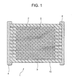
- the multi-layer ceramic capacitor has a capacitor device body (10) of a configuration of dielectric layers (2) and internal electrode layers (3) layered alternately.
- the capacitor device body (10) is not limited to one particular shape, but is normally made in a parallelepiped shape. Further, the capacitor dimensions are not limited and may be made with suitable dimensions for with the application. Usually, however, the dimensions are (0.6 to 5.6 mm) x (0.3 to 5.0 mm) x (0.3 to 1.9 mm).
- the internal electrode layers (3) are stacked so that the end faces thereof alternately protrude out to the surfaces of the two opposing ends of the capacitor device body (10).
- the pair of external electrodes (4) are formed at the two ends of the capacitor device body (10) and are connected to the exposed end faces of the alternately arranged internal electrode layers (3) so as to compose the capacitor circuit.
- the dielectric layer (2) contains a dielectric ceramic composition of the present invention.
- a dielectric ceramic composition of the present invention is comprised of:
- the number of moles of the fourth subcomponent and fifth subcomponent with respect to 100 moles of BaTiO 3 as a main component are expressed by X and Y coordinates
- the number of moles of the fourth subcomponent and fifth subcomponent with respect to 100 moles of BaTiO 3 as a main component are expressed by an X and Y coordinates
- the above ratio of the fourth subcomponent is not the molar ratio of the R1 oxide, but the molar ratio of R1 alone. That is when, for example, using an oxide of Yb as the fourth subcomponent, a ratio of the fourth subcomponent of 1 mole does not mean the ratio of the Yb 2 O 3 is 1 mole, but the ratio of Yb is 1 mole.
- the oxides constituting the main component and the subcomponents are expressed by stoichiochemical compositions, but the oxidized state of the oxides may also deviate from the stoichiochemical compositions.
- the ratios of the subcomponents are found by a conversion from the amounts of the metals contained in the oxides constituting the subcomponents to the oxides of the above stoichiochemical compositions.
- the ratios of the oxides in the first subcomponent may be any ratios.
- the amount of the second subcomponent (containing silicone oxide as a main component) is too small, the capacity-temperature characteristic becomes poor and the IR (specific insulation resistance) falls. On the other hand, if the amount is too large, the IR lifetime becomes insufficient and the dielectric constant ends up falling rapidly.
- the second subcomponent is indicated by at least one selected from SiO 2 , MO (note that M is at least one element selected from Ba, Ca, Sr and Mg), Li 2 O and B 2 O 3 .
- the second subcomponent acts mainly as a sintering promoting agent and has the effect of improving the error rate of initial insulation resistance in the case of thin films.
- the BaO and the CaO in the second subcomponent [(Ba, Ca) x SiO 2+x ] are also contained in the first subcomponent, but the composite oxide (Ba, Ca) x SiO 2+x has a low melting point, so it has good reactivity with the main component. Therefore, in the present invention, the BaO and/or CaO are also added as the above composite oxide.
- the x in the (Ba, Ca) x SiO 2+x as a more preferable state of the second subcomponent is preferably 0.8 to 1.2, more preferably 0.9 to 1.1.
- the ratio of Ba and Ca in the second subcomponent may be any and a subcomponent containing just one is also possible.
- the third subcomponent (V 2 O 5 , MoO 3 , and WO 3 ) exhibits the effect of smoothing the capacity-temperature characteristic higher than the Curie temperature and has the effect of improving the IR lifetime. If the amount of the third subcomponent is too small, the effect becomes insufficient. On the other hand, if the amount is too large, the IR falls remarkably. Note that the ratio of the oxides in the third subcomponent may be any.
- the fourth subcomponent exhibits the effect of shifting the Curie temperature to the high temperature side and has the effect of smoothing the capacity-temperature characteristic. If the amount of the fourth subcomponent is too small, these effects become insufficient and the capacity-temperature characteristic is deteriorated. On the other hand, if the amount is too large, the sinterability tends to deteriorate.
- Yb oxide is preferred since it has a large effect on improvement of the characteristic and is also inexpensive.
- the fifth subcomponent (CaZrO 3 ) displays the effect of shifting the Curie temperature to the higher temperature side and has the effect of making the capacity-temperature characteristics flat. Also, there is the effect of improving the CR product and direct-current insulation break down strength. Note that if the amount of the fifth subcomponent is too much, the IR accelerating lifetime remarkably deteriorates and the capacity-temperature characteristics (X8R characteristics) deteriorate.
- the adding form of CaZrO 3 is not limited specifically and oxides comprised of Ca, such as CaO, a carbonate like CaCO 3 , organic composite, CaZrO 3 , etc. can be raised.
- the ratio of Ca and Zr is not limited specifically and may be determined to the extent that BaTiO 3 as a main component is not made to be a solid solution, but the mole ratio of Ca with respect to Zr (Ca/Zr) is preferably 0.5 to 1.5, more preferably, 0.8 to 1.5, and further preferably, 0.9 to 1.1.
- the capacity-temperature characteristics (X8R characteristics) can be made flat, and a high temperature accelerating lifetime and CR product can be improved. Particularly, in the above value range, deposit of different phases can be prevented and the texture can be unified.
- the amount of the fourth subcomponent is too much, it is possible that a pyrochlore phase of huge needle-shaped crystalline may be deposited and tremendous deterioration of characteristics (decrease of CR product) is observed when the thickness between dielectric layers of a multi-layer ceramic capacitor is made thinner.
- the amount of the fourth subcomponent is too small, the capacity-temperature characteristics cannot be satisfied.
- the amount of the fifth subcomponent is too small, the CR product and the direct-current break down voltage VB are improved while the capacity-temperature characteristics decline and the IR acceleration lifetime also declines.
- a dielectric ceramic composition of the present invention preferably includes an oxide of R2 (note that R2 is at least one element selected from Y, Dy, Ho, Tb, Gd and Eu) for 9 moles or less (more preferably, 0.5 to 9 moles) as a sixth subcomponent.
- the sixth subcomponent (an oxide of R2) displays the effect of improving the IR and IR lifetime and has little adverse effect on the capacity-temperature characteristics. Note that if the amount of the R2 oxide is too large, however, the sinterability tends to deteriorate.
- Y oxide is preferred since it has a large effect on improving the characteristic and is also inexpensive.
- the total amount of the fourth subcomponent and the sixth subcomponent with respect to 100 moles of the main component of BaTiO 3 is preferably not more than 13 moles, and more preferably, not more than 10 moles (note that the numbers of moles of the fourth subcomponent and the sixth subcomponent are ratios of R1 and R2 alone). This is to maintain the preferable sinterability.
- the dielectric ceramic composition of the present invention may contain, as a seventh subcomponent, MnO.
- This seventh subcomponent exhibits the effect of promoting sintering, the effect of increasing the IR and the effect of improving the IR lifetime.
- the ratio of the seventh subcomponent with respect to 100 moles of the BaTiO 3 is preferably at least 0.01 mole. If the amount of the seventh subcomponent is too large, there is an adverse effect on the capacity-temperature characteristic, so the amount is preferably not more than 0.5 mole.
- the dielectric ceramic composition of the present invention may also contain Al 2 O 3 in addition to the above oxides.
- Al 2 O 3 does not have much of an effect on the capacity-temperature characteristic and exhibits the effect of improving sinterability, the IR and the IR lifetime. If the amount of the Al 2 O 3 is too large, however, the sinterability deteriorates and the IR falls, so the Al 2 O 3 is preferably included in an amount of not more than 1 mole with respect to 100 moles of the BaTiO 3 , and more preferably not more than 1 mole in the dielectric ceramic composition as a whole.
- the average grain size of the dielectric ceramic composition of the present invention is not limited and may be determined in accordance with the thickness of the dielectric layers etc. from a range, for example, of 0.1 to 3.0 ⁇ m.
- the dielectric ceramic composition of the present invention is particularly effective when the average grain size has to be made small, specifically, when the average grain size is 0.1 to 0.5 ⁇ m.
- the average grain size small, the IR lifetime becomes longer and the change in the capacity under a direct current electric field over time becomes smaller. Therefore, it is even more preferable that the average grain size is made small for the above reason.
- the Curie temperature of the dielectric ceramic composition of the present invention may be changed by selecting the composition, but in order to satisfy the X8R characteristic, it is preferably at least 120°C, more preferably at least 123°C. Note that the Curie temperature may be measured using a DSC (differential scan calorimetry), etc.
- the thickness of the dielectric layers comprised of the dielectric ceramic composition of the present invention is normally not more than 40 ⁇ m, particularly not more than 30 ⁇ m, per layer.
- the lower limit of the thickness is normally about 2 ⁇ m.
- the dielectric ceramic composition of the present invention is effective for the improvement of the capacity-temperature characteristic of a multi-layer ceramic capacitor having such thinned dielectric layers. Note that the number of the stacked dielectric layers is normally around 2 to 300.
- the dielectric layers are normally subjected to an alternating current electric field of from 0.02V/ ⁇ m, in particular from 0.2V/ ⁇ m, further from 0.5V/ ⁇ m, to generally not more than 5V/ ⁇ m and a direct current electric field of not more than 5V/ ⁇ m superposed over this, but the temperature characteristic of the capacity is extremely stable even when such electric fields are applied.
- the dielectric ceramic composition of the present invention is a dielectric ceramic composition containing as the main component BaTiO 3 , and includes components fulfilling conditions described below in an X-ray diffraction using a Cu-K ⁇ ray.
- the pseudo cubic peak here means a peak where the difference of a lattice constant between the peak of the (002) crystal surface and the peak of the (200) crystal surface disappears and separation by an X-ray diffraction analysis becomes difficult.
- the capacity-temperature characteristics can be improved and the X8R characteristics can be satisfied.
- the measurement conditions at the X-ray diffraction are not specifically limited, but measurement conditions of a scan width of 0.05° or less and a scan speed of 0.1°/minute or less, and as X-ray detection conditions, a parallel slit of 1° or less, an emission slit of 1° or less, and a light receiving slit of 0.3mm or less may usually be used so as to obtain resolution to an extent that the half-width above can be confirmed.
- a dielectric ceramic composition containing the first to fifth subcomponents above as essential components is capable of fulfilling the above conditions in the X-ray diffraction, but a dielectric ceramic composition having other compositions is also capable of fulfilling the above conditions in the X-ray diffraction by appropriately controlling the composition and the production conditions.
- the present invention includes dielectric ceramic compositions containing as the main component BaTiO 3 , which exhibits the characteristics below in the differential scan calorimetry (DSC).
- the DSC is a measuring method for obtaining relationship of temperature and heat flow difference per unit time (dq/dt) which is used for measuring the Curie temperature, etc.
- the value of differentiating the heat flow difference with the temperature (hereinafter, referred to as DDSC) becomes 0 in the Curie temperature.
- DDSC differential scan calorimetry
- a dielectric ceramic composition containing the above first to fifth subcomponents as essential components is capable of fulfilling the above characteristics in the DSC, however, a dielectric ceramic composition having other compositions is also capable of fulfilling the above conditions in the DSC by appropriately controlling the composition and the production conditions.
- the present invention includes dielectric ceramic compositions containing as the main component BaTiO 3 , which exhibits the characteristics below in the Raman spectrum method.
- the first condition is, when measuring by changing the sample temperature and supposing that a Raman peak intensity at 270cm -1 being I 270 and that at 310cm -1 being I 310 at the sample temperature of 130°C, 0.1 ⁇ (I 310 /I 270 ) stands.
- the second condition is, when measuring by changing the sample temperature, a half width value of the Raman peak at 535cm -1 at the sample temperature of 130°C is not more than 95cm -1 .
- the capacity-temperature characteristics are improved and the X8R characteristics can be satisfied.
- measurement conditions of the Raman spectrum method are not specifically limited as far as being able to obtain a resolution so that the above half-width can be confirmed.
- a dielectric ceramic composition containing the above first to fifth subcomponents as essential components is capable of fulfilling the above characteristics in the Raman method, however, a dielectric ceramic composition having other compositions is also capable of fulfilling the above conditions in the Raman method by appropriately controlling the composition and the production conditions.
- the electroconductive material contained in the internal electrode layers (3) is not particularly limited, but a base metal may be used since the material constituting the dielectric layers (2) has a resistance to reduction.
- a base metal may be used since the material constituting the dielectric layers (2) has a resistance to reduction.
- Ni or an Ni alloy is preferable.
- Ni alloy an alloy of at least one type of element selected from Mn, Cr, Co, and Al with Ni is preferable.
- the amount of the Ni in the alloy is preferably not less than 95 wt%.
- Ni or Ni alloy may contain P and other various types of trace components in amounts of not more than 0.1 wt% or so.
- the thickness of the internal electrode layer may be suitably determined in accordance with the application etc., but is usually 0.5 to 5 ⁇ m, in particular 0.5 to 2.5 ⁇ m.
- the electroconductive material contained in the external electrodes (4) is not particularly limited, but in the present invention an inexpensive Ni, Cu, or alloys of the same may be used.
- the thickness of the external electrodes may be suitably determined in accordance with the application etc., but is usually around 10 to 50 ⁇ m.
- the multi-layer ceramic capacitor using the dielectric ceramic composition of the present invention is produced by preparing a green chip using the usual printing method or sheet method which uses pastes, firing the green chip, then printing or transferring and firing the external electrodes. The method of manufacture will be explained in detail below.
- the dielectric layer paste may be an organic-based paint comprised of a mixture of a dielectric ingredient and an organic vehicle and may also be a water-based paint.
- the dielectric ingredient use may be made of the above-mentioned oxides or mixtures thereof or composite oxides, but it is also possible to use one selected from various compounds or mixtures becoming the above oxides or composite oxides after firing, such as carbonates, oxalates, nitrates, hydroxides and organic metal compounds.
- the amount quantity of the compounds in the dielectric ingredient may be suitably determined so as to give the above-mentioned composition of the dielectric ceramic composition after firing.
- the dielectric ingredient is normally used as a powder of an average particle size of 0.1 to 3 ⁇ m.
- the organic vehicle is comprised of a binder dissolved in an organic solvent.
- the binder used for the organic vehicle is not particularly limited, but may be suitably selected from ethyl cellulose, polyvinyl butyral, and other ordinary types of binders.
- the organic solvent used is also not particularly limited and may be suitably selected from terpineol, butyl carbitol, acetone, toluene and other organic solvents in accordance with the printing method, sheet method, or other methods of use.
- a water-based paint as the dielectric layer paste, it is sufficient to knead a water-based vehicle comprised of a water-based binder or dispersant, etc. dissolved in water together with the dielectric layer ingredient.
- the water-based binder used for the water-based vehicle is not particularly limited.
- a polyvinyl alcohol, cellulose, water-based acrylic resin, etc. may be used.
- the internal electrode layer paste is prepared by kneading the electroconductive material comprised of the above various types of electroconductive metals and alloys or various types of oxides becoming the above electroconductive materials after firing, an organic metal compound, resinate, etc. together with the above organic vehicle.
- the external electrode paste may be prepared in the same way as the above internal electrode layer paste.
- the amount of the organic vehicle in the above pastes is not particularly limited and may fall within the usual amount, for example, the binder may be contained in an amount of 1 to 5 wt% or so and the solvent 10 to 50 wt% or so. Further, the pastes may include, in accordance with need, various types of additives selected from dispersants, plasticizers, dielectrics, insulators, etc. The total amount of these is preferably not more than 10 wt%.
- the dielectric layer paste and the internal electrode layer paste are successively printed on the PET or other substrate.
- the result is then cut into a predetermined shape, afterwhich the pastes are peeled off from the substrate to form a green chip.
- a dielectric layer paste is used to form a green sheet, the internal electrode layer paste is printed on upper surface of this, afterwhich these are layered to form a green chip.
- the green chip is processed to remove the binder.
- This process for removing the binder may be performed under ordinary conditions, but when using Ni or a Ni alloy or other base metal for the electroconductive material of the internal electrode layer, this is preferably performed under conditions where the air atmosphere has a rate of temperature rise of 5 to 300°C/hour, in particular 10 to 100°C/hour, a holding temperature is 180 to 400°C, in particular 200 to 300°C and a temperature holding time is 0.5 to 24 hours, in particular 5 to 20 hours.
- the atmosphere when firing the green chip may be suitably determined in accordance with the type of electroconductive material in the internal electrode layer paste, but when using Ni or a Ni alloy or other base metal as the electroconductive material, the oxygen partial pressure in the firing atmosphere is preferably 10 -8 to 10 -15 atms. If the oxygen partial pressure is less than this range, the electroconductive material of the internal electrode layers becomes abnormally sintered and ends up breaking in the middle in some cases. Further, if the oxygen partial pressure exceeds the above range, the internal electrode layers tend to become oxidized.
- the holding temperature at the time of firing is preferably 1100 to 1400°C, more preferably 1200 to 1360°C, still more preferably 1200 to 1320°C. If the holding temperature is less than the above range, the densification becomes insufficient, while if over that range, there is a tendency toward breaking of the electrodes due to abnormal sintering of the internal electrode layers, deterioration of the capacity-temperature characteristic due to dispersion of the material comprising the internal electrode layers and reduction of the dielectric ceramic composition.
- the various conditions other than the above conditions are that preferably the rate of temperature rise is 50 to 500°C/hour, in particular 200 to 300°C/hour, a temperature holding time is 0.5 to 8 hours, in particular 1 to 3 hours, the cooling rate is 50 to 500°C/hour, in particular 200 to 300°C/hour.
- the firing atmosphere is preferably a reducing atmosphere.
- the atmospheric gas it is preferable to use for example, a wet mixed gas of N 2 and H 2 .
- the capacitor device body When firing in a reducing atmosphere, the capacitor device body is preferably annealed.
- the annealing process is for re-oxidizing the dielectric layer. Since this enables the IR lifetime to be remarkably prolonged, reliability is improved.
- the oxygen partial pressure in the annealing atmosphere is preferably not less than 10 -9 atms, in particular 10 -6 to 10 -9 atms. If the oxygen partial pressure is less than the above range, re-oxidation of the dielectric layer is difficult, while if over that range, the internal electrode layers tend to become oxidized.
- the holding temperature at the time of annealing is preferably not more than 1100°C, in particular 500 to 1100°C. If the holding temperature is less than the above range, oxidation of the dielectric layers becomes insufficient, so the IR tends to become low and the IR lifetime short. On the other hand, when the holding temperature exceeds the above range, not only do the internal electrode layers oxidize and the capacity fall, but also the internal electrode layers end up reacting with the dielectric material resulting in a tendency toward deterioration of the capacity-temperature characteristic, a fall in the IR and a fall in the IR lifetime.
- the annealing may be comprised of only a temperature raising process and temperature reducing process. That is, the temperature holding time may also be zero. In this case, the holding temperature is synonymous with the maximum temperature.
- the various conditions other than the above conditions in annealing are that the temperature holding time is preferably 0 to 20 hours, in particular 6 to 10 hours, the cooling rate is preferably 50 to 500°C/hour, in particular 100 to 300°C/hour. Note that for the atmospheric gas, wet N 2 gas, etc. may be used.
- the temperature of the water is preferably 5 to 75°C.
- the process for removing the binder, firing, and annealing may be performed consecutively or independently.
- the atmosphere is changed without cooling, then the temperature is raised to the holding temperature for firing, the firing performed, then the chip is cooled, the atmosphere is changed when the holding temperature of the annealing is reached, and then annealing is performed.
- the temperature is raised to the holding temperature at the time of the process for removing the binder in an N 2 gas or wet N 2 gas atmosphere, then the atmosphere is changed and the temperature is further raised.
- the chip is cooled to the holding temperature of the annealing, then the atmosphere is changed again to an N 2 gas or wet N 2 gas atmosphere and the cooling continued. Further, at the time of annealing, the temperature may be raised to the holding temperature in an N 2 gas atmosphere, afterwhich the atmosphere is changed or the entire annealing process may be performed in a wet N 2 gas atmosphere.
- the thus obtained capacitor device body is, for example, end polished using barrel polishing or sandblasting etc., then printed or transferred with an external electrode paste and fired to form the external electrodes 4.
- the firing conditions of the external electrode paste are for example preferably 600 to 800°C for 10 minutes to 1 hour or so in a wet mixed gas of N 2 and H 2 .
- the surfaces of the external electrodes 4 may be formed with a covering layer using plating techniques, etc.
- the thus produced multi-layer ceramic capacitor of the present invention is mounted by soldering it onto a printed circuit board for use in various types of electronic equipment.
- illustration was made of a multi-layer ceramic capacitor as the electronic device according to the present invention, but the electronic device according to the present invention is not limited to a multi-layer ceramic capacitor and may be any device having a dielectric layer comprised of a dielectric ceramic composition of the above composition.
- a main component material (BaTiO 3 ) and the first to seventh subcomponents respectively having an average particle diameter of 0.1 to 1 ⁇ m were prepared.
- Carbonate (the first subcomponent: MgCO 3 , the seventh subcomponent: MnCO 3 ) was used for a material of MgO and MnO, and oxides (the second subcomponent: (Ba 0.6 Ca 0.4 )SiO 3 , the third subcomponent: V 2 O 5 , the fourth subcomponent:Yb 2 O 3 , the fifth subcomponent:CaZrO 3 , the sixth subcomponent: Y 2 O 3 ) were used as other materials.
- (Ba 0.6 Ca 0.4 ) SiO 3 as the second subcomponent was prepared by performing wet mixing using a ball mill for 16 hours on BaCO 3 , CaCO 3 and SiO 2 , drying, firing at 1150°C in the air, and further performing wet grinding using a ball mill for 100 hours.
- CaZrO 3 as the fifth subcomponent was prepared by performing wet mixing using a ball mill for 16 hours on CaCO 3 and ZrO 3 , drying, firing at 1150°C in the air, and further performing wet grinding using a ball mill for 24 hours.
- the same characteristics were also obtained by using the main component BaTiO 3 prepared by respectively weighing BaCO 3 and TiO 2 , performing wet mixing using a ball mill for 16 hours on CaCO 3 and ZrO 2 , drying, firing at 1100°C in the air, and further performing wet grinding using a ball mill for 16 hours. Also, the same characteristics were obtained by using the main component BaTiO 3 prepared using hydrothermal crystallization powder, an oxalate method, etc.
- Table 1 Sample Main Component Subcomponent Number First Second Third Fourth Fifth Sixth Seventh BaTiO 3 MgCO 3 (Ba 0.6 .
- a dielectric paste was prepared by mixing through use of a ball mill to make a paste 100 parts by weight of the thus obtained dried dielectric materials, 4.8 parts by weight of acrylic resin, 40 parts by weight of methylene chloride, 20 parts by weight of ethyl acetate, 6 parts by weight of mineral spirits and 4 parts by weight of acetone.
- an internal electrode paste was made by kneading using a triple-roll to make a paste 100 parts by weight of Ni particles of an average particle size of 0.2 to 0.8 ⁇ m, 40 parts by weight of an organic vehicle (8 parts by weight of an ethyl cellulose resin dissolved in 92 parts by weight of butyl carbitol), and 10 parts by weight of butyl carbitol.
- An external electrode paste was prepared by kneading together to make a paste 100 parts by weight of Cu particles of an average particle size of 0.5 ⁇ m, 35 parts by weight of an organic vehicle (8 parts by weight of an ethyl cellulose resin dissolved in 92 parts by weight of butyl carbitol) and 7 parts by weight of butyl carbitol.
- the above dielectric layer paste was used to form a green sheet having a thickness of 15 ⁇ m on a PET film.
- An internal electrode paste was printed on this, then the sheet was peeled from the PET film.
- the thus obtained green sheets and protection green sheet (on which the internal electrode layer paste is not printed) were layered, adhered by means of pressure to prepare a green chip.
- the number of layered layers of the green sheet having the internal electrode was four.
- the green chip was cut to a predetermined size and was processed to remove the binder, fired, and annealed to obtain the multi-layer ceramic fired body.
- the process of removing the binder was performed under conditions where a time of temperature rise was 15°C/hour, a holding temperature was 280°C, a holding time was 8 hours and in the air atmosphere. Firing was performed under the conditions where the rate of temperature rise was 200°C/hour, a holding temperature was 1280 to 1320°C, a holding time was 2 hours, the rate of cooling was 300°, and in an atmosphere of wet mixed gas of N 2 +H 2 (an oxygen partial pressure was 10 -9 atms.
- Annealing was performed under the conditions that a holding temperature was 900°C, a temperature holding time was 9 hours, and in a wet N 2 gas atmosphere (an oxygen partial pressure was 10 -5 atms). Note that a wetter having a water temperature of 35°C was used for wetting the atmosphere gases at the time of firing and annealing.
- the external electrodes were formed by polishing the end faces of the fired body by sandblasting, then transferring the external electrode paste to the end faces and firing them there in a wet N 2 +H 2 atmosphere at 800°C for 10 minutes, so as to obtain a sample of a multi-layer ceramic capacitor having the configuration as shown in FIG. 1 .
- the size of the thus obtained respective samples was 3.2mm x 1.6mm x 0.6mm, the number dielectric layers sandwiched by the internal electrode layers was 4 and the thickness thereof was 10 ⁇ m, and the thickness of the internal electrode layer was 2 ⁇ m.
- Disk-shaped samples were prepared in addition to the samples of the capacitors.
- the disk-shaped samples have the same composition as that of the above capacitors, have the same firing conditions, and an In-Ga electrode having a diameter of 5mm was applied on the both surfaces of the samples.
- the capacitance and dielectric loss were measured by an LCR meter under conditions of a frequency of 1 kHz and an input signal level of 1 Vrms. Then, the permittivity (no unit) was calculated from the obtained capacitance, an electrode size and a distance between electrodes. A direct-current of 50V was applied for one minute at 25°C, the specific insulation resistance (IR, unit of ⁇ cm) at the time was measured using an insulator resistance meter (R8340A made by Advantest Co.), and a CR product was calculated. The CR product was indicated by a product of the capacitance (C, ⁇ F) with the specific insulation resistance (R, M ⁇ ). The result is shown in Table 2.
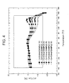
- Samples containing CaZro 3 (Samples 10, 14, 23, 25, 33 and 39) in embodiments of the present invention were selected and the capacity temperature characteristics of -55°C to 160°C of those were shown in FIG. 4 .
- a block range fulfilling the X8R characteristics is also shown in FIG. 4 . Note that an LCR meter was used for measurement and the measurement voltage was set to be 1V.
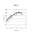
- capacitor samples (Samples 5, 10, 14, 18, 23, 28, 33 and 39) in embodiments of the present invention were selected and the relationship between the amount of CaZrO 3 and the Curie temperature (measured by DSC) thereof were shown in FIG. 5 .
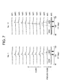
- Cu-K ⁇ powder X-ray
- the capacitor sample containing CaZrO 3 inside the range of the present invention (Sample 17) and the capacitor samples containing CaZrO 3 outside the composition range of the present invention (Samples 1, 2, 3 to 24) were used for measuring changes of capacitance ( ⁇ cp) where a direct-current voltage was gradually applied to the respective samples at a constant temperature (25°C). The result is shown in FIG. 8 .
- composition of Sample 2 was 85BaTiO 3 +1Bi 2 O 3 +4.5Ta 2 O 6 +0.5MgO+1CuO+1.5ZnO+2TiO 2 +1.5SnO 2 +3Dy 2 O 3 and the composition of Samples 3 to 24 was 98BaTiO 3 +2CaTiO 3 +Nb 2 O 5 (1wt%) +ZnO (1wt%) +MnO (1wt%) +SiO 2 (1w t%).
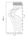
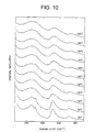
- Example 1 The disk-shaped samples (Samples 1, 5, 10, 14, 18, 23, 28, 33 and 39) were measured for their heat absorbing peak by the DSC so as to obtain a Curie temperature. Also, the half-width of the heat absorbing peak in the temperature-DSC graph was obtained. The results are shown in Table 4. Temperature-DDSC curves of samples in Table 4 are shown in FIG. 9 .
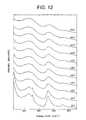
- the sample temperature of the disk-shaped samples was raised to 25°C, 50°C, 120°C, 125°C, 130°C, 135°C, 140°C, 145°C and 150°C by means of a temperature rise rate of 0.5°C/min. Which was further raised between 160°C and 200°C at a temperature rise of 1°C/min. by means of a Raman spectrum analysis apparatus (note that the temperatures were held for 20 minutes after reaching the determined temperatures).
- a single color light was emitted from a light source on the samples at the respective temperatures and a Raman peak position (unit is cm -1 ), a half-width (unit is cm -1 ), peak intensity (CPS) and relative peak intensity were measured or calculated.
- the measurement conditions were that the light source for emission was arranged so that an emission angle with respect to the sample became about 60° and a light having an exciting wavelength of 514.5nm, a laser power of 50mW and having slits of 100 ⁇ m was emitted.
- the results at the sample temperature of 130°C is shown in Table 5.
- the samples of the present embodiment have a dielectric loss (tan ⁇ ) of not more than 10%, a specific insulation resistance (IR) of 1x10 12 ⁇ cm or more, a CR product of 500 M ⁇ f or more, and have an excellent capacitor characteristics.
- Samples were prepared in the same way as in Sample 17 in the example 1 except that the ratio of Ca to Zr in CaZrO 3 as the fifth subcomponent was changed by 0.1 from 0.5 to 1.5. The same measurements as in the example 1 were made on the samples. It was confirmed that the effect of the present invention was realized regardless of the ratio of Ca and Zr in the seventh subcomponent.
- sample 17-1 was prepared in the same way as in the Sample 17 in the example 1 as shown in Table 9 except that the Y 2 O 3 as the sixth subcomponent was increased by 2.5 moles (5 moles in Y conversion).
- the same measurements as in the example 1 were made on the sample.
- the results are shown in Tables 10 and 11 and almost the same results as in the example 1 were obtained. Note that it was confirmed that no adverse effects on other characteristics were observed even if an additional amount of Y 2 O 3 was added.
- sample 17-2 was prepared in the same way as in the Sample 17 in the example 1 as shown in Table 9 except that the Y 2 O 3 as the sixth subcomponent was not added.
- the same measurements as in the example 1 were made on the sample.
- the results are shown in Tables 10 and 11 and almost the same results as in the example 1 were obtained.
- a sample (Sample 17-3) was prepared in the same way as in the Sample 17 in the example 1 as shown in Table 9 except that the MnCO 3 as the seventh subcomponent was not added.
- the same measurements as in the example 1 were made on the sample. The results are shown in Tables 10 and 11 and almost the same results as in the example 1 were obtained.
Landscapes
- Engineering & Computer Science (AREA)
- Chemical & Material Sciences (AREA)
- Ceramic Engineering (AREA)
- Power Engineering (AREA)
- Manufacturing & Machinery (AREA)
- Microelectronics & Electronic Packaging (AREA)
- Inorganic Chemistry (AREA)
- Organic Chemistry (AREA)
- Structural Engineering (AREA)
- Materials Engineering (AREA)
- Compositions Of Oxide Ceramics (AREA)
- Inorganic Insulating Materials (AREA)
- Ceramic Capacitors (AREA)
Claims (15)
- Composition de céramique diélectrique, comprenant :un composant principal constitué principalement de titanate de baryum,un premier sous-composant, qui est au moins un composé choisi parmi MgO, CaO, BaO, SrO et Cr2O3,un deuxième sous-composant contenant de l'oxyde de silicium comme composition principale,un troisième sous-composant, qui est au moins un composé choisi parmi V2O5, MoO3 et WO3,un quatrième sous-composant, qui est un oxyde de R1, où R1 est au moins un élément choisi parmi Sc, Er, Tm, Yb et Lu, etun cinquième sous-composant, qui est CaZrO3 ou CaO+ZrO2, où les rapports des sous-composants pour 100 moles du composant principal, qui est constitué principalement de titanate de baryum, sont :0,1 à 3 moles pour le premier sous-composant,2 à 10 moles pour le deuxième sous-composant,0,01 à 0,5 mole pour le troisième sous-composant,0,5 à 7 moles pour le quatrième sous-composant, le nombre de moles du quatrième sous-composant étant le rapport de R1 seul, et0 < cinquième sous-composant ≤ 5 moles pour le cinquième sous-composant.
- Composition de céramique diélectrique selon la revendication 1, dans laquelle, lorsque le nombre de moles du quatrième sous-composant et du cinquième sous-composant, par rapport à 100 moles du composant principal qui est principalement constitué de titanate de baryum, le nombre de moles du quatrième sous-composant étant le rapport de R1 seul, est exprimé par des coordonnées X, Y, le nombre de moles du quatrième sous-composant et celui du cinquième sous-composant répondent à une relation correspondant à la plage entourée par des lignes droites de Y=5, Y=0, Y=(2/3)X-(7/ 3), X=0,5 et X=5, la limite de Y=0 n'étant pas incluse.
- Composition de céramique diélectrique selon la revendication 1, dans laquelle, lorsque le nombre de moles du quatrième sous-composant et du cinquième sous-composant, par rapport à 100 moles du composant principal qui est principalement constitué de titanate de baryum, le nombre de moles du quatrième sous-composant étant le rapport de R1 seul, est exprimé par des coordonnées X, Y, le nombre de moles du quatrième sous-composant et celui du cinquième sous-composant répondent à la relation correspondant à la plage entourée par des lignes droites de Y=5, Y=0, Y=(2/3)X-(7/ 3), Y=-(1,5)X+9,5, X=1 et X=5, la limite de Y=0 n'étant pas incluse.
- Composition de céramique diélectrique selon la revendication 1, 2 ou 3, comprenant un sixième sous-composant, à savoir un oxyde de R2, où R2 est au moins un élément choisi parmi Y, Dy, Ho, Tb, Gd et Eu, et une quantité dudit sixième sous-composant n'est pas supérieure à 9 moles par rapport à 100 moles du composant principal, qui est principalement constitué de titanate de baryum, le nombre de moles du sixième sous-composant étant le rapport de R2 seul.
- Composition selon la revendication 4, dans laquelle une quantité totale des quatrième et sixième sous-composants n'est pas supérieure à 13 moles par rapport à 100 moles du composant principal, qui est principalement constitué de titanate de baryum, les nombres de moles des quatrième et sixième sous-composants étant respectivement les rapports de R1 et R2 seuls.
- Composition selon l'une quelconque des revendications 1 à 5,
dans laquelle ledit deuxième sous-composant est au moins un composé choisi parmi SiO2, Li2O, B2O3 et MO, M étant au moins un élément choisi parmi Ba, Ca, Sr et Mg. - Composition selon l'une quelconque des revendications 1 à 6,
comprenant en outre un septième sous-composant MnO, la quantité du septième sous-composant n'étant pas supérieure à 0,5 mole par rapport à 100 moles du composant principal qui est principalement constitué de titanate de baryum. - Composition de céramique diélectrique selon la revendication 1, dans laquelle,
lorsqu'une valeur d'une différence de flux de chaleur (dq/dt) par unité de temps, mesurée par DSC (calorimétrie à balayage différentiel), qui est différenciée par une température, est définie comme étant une DDSC (calorimétrie différentielle différenciée par la température), une différence de température entre une paire de pics, qui existe de part et d'autre de la température de Curie, n'est pas inférieure à 4,1 °C sur un graphique montrant la relation entre la température et la DDSC (calorimétrie différentielle différenciée par la température). - Composition de céramique diélectrique selon la revendication 1, dans laquelle :un pic pseudo-cubique, comprenant un pic d'une surface de cristal (002) et un pic d'une surface de cristal (200), est observé dans une plage de 2θ=44 ° à 46 ° dans une diffraction de rayons X en utilisant une ligne de Cu-Kα ;une demi-largeur dudit pic pseudo-cubique n'est pas inférieure à 0,3 ° à température ambiante ; et,lorsque l'on détermine que l'intensité dudit pic de la surface de cristal (002) est I(002) et que l'intensité dudit pic de la surface de cristal (200) est I(200), on obtient la relation I(002) ≥ I(200).
- Composition de céramique diélectrique selon la revendication 7, dans laquelle :un pic pseudo-cubique, comprenant un pic d'une surface de cristal (004) et un pic d'une surface de cristal (400), est observé dans une plage de 2θ=98 ° à 103 ° dans une diffraction de rayons X en utilisant une ligne de Cu-Kα ; etune demi-largeur dudit pic pseudo-cubique n'est pas inférieure à 0,4 ° à une température de 120 °C.
- Composition de céramique diélectrique selon la revendication 1, dans laquelle :lorsque la composition de céramique diélectrique est mesurée au moyen d'un procédé à spectre de Raman en utilisant diverses températures d'échantillon, que l'intensité du pic de Raman à 270 cm-1 et à 130 °C est définie comme la valseur I270 et que l'intensité du pic de Raman à 310 cm-1 et à 130 °C est définie comme la valeur I310, on obtient 0.1 ≤ (I310/I270) .
- Composition de céramique diélectrique selon la revendication 1, dans laquelle :lorsque la composition de céramique diélectrique est mesurée au moyen d'un procédé à spectre de Raman en utilisant diverses températures d'échantillon,une demi-largeur du pic de Raman à 535 cm-1 n'est pas supérieure à 95 cm-1 à la température d'échantillon de 130 °C.
- Dispositif électrique ayant une couche diélectrique constituée d'une composition de céramique diélectrique selon l'une quelconque des revendications 1 à 12.
- Dispositif électrique selon la revendication 13, comprenant un corps de dispositif capacitif, dans lequel lesdites couches diélectriques et lesdites couches d'électrodes internes sont disposées en couches alternées.
- Dispositif électrique selon la revendication 14, dans lequel un matériau conducteur inclus dans ladite couche d'électrode interne est formée de Ni ou d'un alliage de Ni.
Applications Claiming Priority (4)
| Application Number | Priority Date | Filing Date | Title |
|---|---|---|---|
| JP29726999 | 1999-10-19 | ||
| JP29726999 | 1999-10-19 | ||
| JP2000226862 | 2000-07-27 | ||
| JP2000226862A JP3348081B2 (ja) | 1999-10-19 | 2000-07-27 | 誘電体磁器組成物および電子部品 |
Publications (3)
| Publication Number | Publication Date |
|---|---|
| EP1094477A2 EP1094477A2 (fr) | 2001-04-25 |
| EP1094477A3 EP1094477A3 (fr) | 2006-03-29 |
| EP1094477B1 true EP1094477B1 (fr) | 2009-04-22 |
Family
ID=26561062
Family Applications (1)
| Application Number | Title | Priority Date | Filing Date |
|---|---|---|---|
| EP00122255A Expired - Lifetime EP1094477B1 (fr) | 1999-10-19 | 2000-10-18 | Composition dielectrique céramique et composant électronique |
Country Status (4)
| Country | Link |
|---|---|
| EP (1) | EP1094477B1 (fr) |
| JP (1) | JP3348081B2 (fr) |
| KR (1) | KR100352245B1 (fr) |
| DE (1) | DE60042050D1 (fr) |
Families Citing this family (38)
| Publication number | Priority date | Publication date | Assignee | Title |
|---|---|---|---|---|
| US7482299B2 (en) | 1998-07-29 | 2009-01-27 | Namics Corporation | Dielectric ceramic composition and multi-layer ceramic capacitor |
| JP3341003B2 (ja) | 2000-12-25 | 2002-11-05 | ティーディーケイ株式会社 | 誘電体磁器組成物および電子部品 |
| DE60129533T2 (de) | 2000-12-25 | 2007-11-22 | Tdk Corp. | Dielektrische porzellan zusammensetzung und elektronische teile |
| EP1327616B9 (fr) | 2002-01-15 | 2011-04-13 | TDK Corporation | Composition céramique diélectrique et dispositif électronique |
| JP4534001B2 (ja) * | 2003-12-16 | 2010-09-01 | 独立行政法人物質・材料研究機構 | ジルコニウム酸カルシウム粉末 |
| TW200531955A (en) * | 2004-03-16 | 2005-10-01 | Tdk Corp | Dielectric ceramic composition, multilayer ceramic capacitor, and method for manufacturing the same |
| US7898793B2 (en) | 2004-03-19 | 2011-03-01 | Tdk Corporation | Laminated ceramic capacitor |
| JP2005272262A (ja) * | 2004-03-26 | 2005-10-06 | Tdk Corp | 誘電体磁器組成物、積層型セラミックコンデンサ及びその製造方法 |
| JP2005335963A (ja) * | 2004-05-24 | 2005-12-08 | Matsushita Electric Ind Co Ltd | 誘電体磁器組成物およびそれを用いた積層セラミックコンデンサ |
| JP4203452B2 (ja) * | 2004-06-28 | 2009-01-07 | Tdk株式会社 | 積層型セラミックコンデンサの製造方法 |
| JP5017770B2 (ja) * | 2004-06-28 | 2012-09-05 | Tdk株式会社 | 誘電体磁器組成物および電子部品 |
| JP4095586B2 (ja) | 2004-06-29 | 2008-06-04 | Tdk株式会社 | 積層型セラミックコンデンサおよびその製造方法 |
| TWI275582B (en) | 2004-08-30 | 2007-03-11 | Tdk Corp | Dielectric ceramic composition and electronic device |
| JP4572628B2 (ja) | 2004-08-30 | 2010-11-04 | Tdk株式会社 | 誘電体磁器組成物及び電子部品 |
| JP4206062B2 (ja) | 2004-08-30 | 2009-01-07 | Tdk株式会社 | セラミック電子部品およびその製造方法 |
| JP4275036B2 (ja) * | 2004-08-30 | 2009-06-10 | Tdk株式会社 | 誘電体磁器組成物及び電子部品 |
| JP4295179B2 (ja) | 2004-08-31 | 2009-07-15 | Tdk株式会社 | 電子部品およびその製造方法 |
| JP4701364B2 (ja) * | 2004-11-15 | 2011-06-15 | 独立行政法人 日本原子力研究開発機構 | 誘電体磁器の評価方法 |
| US7277269B2 (en) * | 2004-11-29 | 2007-10-02 | Kemet Electronics Corporation | Refractory metal nickel electrodes for capacitors |
| JP4407497B2 (ja) | 2004-11-30 | 2010-02-03 | Tdk株式会社 | 誘電体磁器組成物及び電子部品 |
| JP4483659B2 (ja) | 2005-04-04 | 2010-06-16 | Tdk株式会社 | 電子部品、誘電体磁器組成物およびその製造方法 |
| JP5017792B2 (ja) * | 2005-04-04 | 2012-09-05 | Tdk株式会社 | 電子部品、誘電体磁器組成物およびその製造方法 |
| JP5167579B2 (ja) * | 2005-07-12 | 2013-03-21 | Tdk株式会社 | 誘電体磁器組成物及び電子部品 |
| JP2007131476A (ja) * | 2005-11-09 | 2007-05-31 | Tdk Corp | 誘電体磁器組成物、電子部品および積層セラミックコンデンサ |
| JP4782551B2 (ja) * | 2005-11-28 | 2011-09-28 | 京セラ株式会社 | 誘電体磁器 |
| JP4299827B2 (ja) * | 2005-12-05 | 2009-07-22 | Tdk株式会社 | 誘電体磁器組成物、電子部品および積層セラミックコンデンサ |
| EP1890303A4 (fr) * | 2006-06-12 | 2010-05-12 | Namics Corp | Composition céramique diélectrique et condensateur céramique stratifié |
| KR100765708B1 (ko) * | 2006-11-15 | 2008-04-02 | 나믹스 코포레이션 | 유전체 자기 조성물 및 적층 세라믹 콘덴서 |
| WO2008088552A2 (fr) * | 2007-01-17 | 2008-07-24 | Ferro Corporation | Composition diélectrique x8r destinée à être utilisée avec des électrodes au nickel |
| JP4931697B2 (ja) * | 2007-05-29 | 2012-05-16 | 京セラ株式会社 | 誘電体磁器およびコンデンサ |
| JP5100592B2 (ja) * | 2008-09-26 | 2012-12-19 | 京セラ株式会社 | 積層セラミックコンデンサ |
| JP5223927B2 (ja) * | 2008-09-30 | 2013-06-26 | 株式会社村田製作所 | チタン酸バリウム系半導体磁器組成物及びptcサーミスタ |
| CN101805178B (zh) * | 2010-01-22 | 2012-06-13 | 华中科技大学 | 一种钛酸钡基半导体陶瓷的高能球磨制备方法 |
| CN104628378B (zh) * | 2015-02-05 | 2017-02-22 | 汕头高新区松田实业有限公司 | 一种可用于铜电极陶瓷电容器的介质及其制备方法 |
| WO2016189003A1 (fr) * | 2015-05-27 | 2016-12-01 | Epcos Ag | Composition diélectrique à base de titanate de bismuth sodium strontium, et élément diélectrique, composant électronique et composant électronique stratifié correspondants |
| CN107851514B (zh) | 2015-05-27 | 2020-08-21 | 爱普科斯公司 | 基于铋钠锶钛酸盐的介电组合物、其介电元件、电子组件和层叠电子组件 |
| CN114133238B (zh) * | 2021-11-02 | 2022-09-16 | 广东省先进陶瓷材料科技有限公司 | 一种陶瓷介质材料及其制备方法和应用 |
| CN114014649B (zh) * | 2021-12-13 | 2023-07-25 | 深圳先进电子材料国际创新研究院 | 共掺杂钛酸钡陶瓷介电材料、制备方法及其应用 |
Family Cites Families (10)
| Publication number | Priority date | Publication date | Assignee | Title |
|---|---|---|---|---|
| DE69009012T2 (de) * | 1989-11-30 | 1994-12-01 | Taiyo Yuden Kk | Festdielektrikum-Kondensator und Verfahren zur Herstellung. |
| US5103370A (en) * | 1989-12-04 | 1992-04-07 | Taiyo Yuden Co., Ltd. | Solid dielectric capacitor and method of manufacture |
| JPH0779004B2 (ja) * | 1990-10-31 | 1995-08-23 | 株式会社村田製作所 | 誘電体磁器組成物 |
| US5319517A (en) * | 1992-03-27 | 1994-06-07 | Tdk Corporation | Multilayer ceramic chip capacitor |
| JP2764513B2 (ja) * | 1993-01-21 | 1998-06-11 | ティーディーケイ株式会社 | 耐還元性誘電体磁器組成物 |
| JP3161278B2 (ja) * | 1995-04-26 | 2001-04-25 | 株式会社村田製作所 | 誘電体磁器組成物 |
| KR100196406B1 (ko) * | 1996-09-10 | 1999-06-15 | 조희재 | 고유전율 유전체 자기조성물 |
| KR19990009793A (ko) * | 1997-07-11 | 1999-02-05 | 조희재 | 온도보상용계 유전체 자기 조성물 |
| DE19737324A1 (de) * | 1997-08-28 | 1999-03-04 | Philips Patentverwaltung | Vielschichtkondensator mit silber- und seltenerdmetalldotiertem Bariumtitanat |
| JP3275799B2 (ja) * | 1997-09-25 | 2002-04-22 | 株式会社村田製作所 | 誘電体磁器組成物 |
-
2000
- 2000-07-27 JP JP2000226862A patent/JP3348081B2/ja not_active Expired - Lifetime
- 2000-10-18 DE DE60042050T patent/DE60042050D1/de not_active Expired - Lifetime
- 2000-10-18 EP EP00122255A patent/EP1094477B1/fr not_active Expired - Lifetime
- 2000-10-19 KR KR1020000061624A patent/KR100352245B1/ko not_active Expired - Lifetime
Also Published As
| Publication number | Publication date |
|---|---|
| KR20010051144A (ko) | 2001-06-25 |
| JP3348081B2 (ja) | 2002-11-20 |
| KR100352245B1 (ko) | 2002-09-12 |
| JP2001192264A (ja) | 2001-07-17 |
| DE60042050D1 (de) | 2009-06-04 |
| EP1094477A2 (fr) | 2001-04-25 |
| EP1094477A3 (fr) | 2006-03-29 |
Similar Documents
| Publication | Publication Date | Title |
|---|---|---|
| EP1094477B1 (fr) | Composition dielectrique céramique et composant électronique | |
| US6403513B1 (en) | Dielectric ceramic composition and electronic device | |
| EP0977218B1 (fr) | Composition céramique diélectrique et composant électronique | |
| EP1070685B1 (fr) | Composition céramique diélectrique et dispositif électronique | |
| EP1146024B1 (fr) | Procede de production de composition ceramique dielectrique | |
| EP1635360B1 (fr) | Composition en céramique diélectrique et dispositif électronique | |
| EP1327616A2 (fr) | Composition céramique diélectrique et dispositif électronique | |
| US6764976B2 (en) | Dielectric ceramic composition and electronic device | |
| JP3340722B2 (ja) | 誘電体磁器組成物の製造方法 | |
| EP1138652A1 (fr) | Procédé de production d'une composition céramique et procédé de fabrication d'un dispositif électronique | |
| EP1710817B1 (fr) | Dispositif électronique, composition de céramique diélectrique et procédé de fabrication | |
| EP1630833B1 (fr) | Composition en céramique diélectrique et dispositif électronique | |
| EP1736456A1 (fr) | Condensateur ceramique stratifie | |
| JP3340723B2 (ja) | 誘電体磁器組成物の製造方法 | |
| EP1138651A1 (fr) | Procédé de production d'une composition céramique et procédé de fabrication d'un dispositif électronique | |
| JP2001135544A (ja) | 誘電体磁器組成物および電子部品 |
Legal Events
| Date | Code | Title | Description |
|---|---|---|---|
| PUAI | Public reference made under article 153(3) epc to a published international application that has entered the european phase |
Free format text: ORIGINAL CODE: 0009012 |
|
| 17P | Request for examination filed |
Effective date: 20001116 |
|
| AK | Designated contracting states |
Kind code of ref document: A2 Designated state(s): AT BE CH CY DE DK ES FI FR GB GR IE IT LI LU MC NL PT SE |
|
| AX | Request for extension of the european patent |
Free format text: AL;LT;LV;MK;RO;SI |
|
| PUAL | Search report despatched |
Free format text: ORIGINAL CODE: 0009013 |
|
| AK | Designated contracting states |
Kind code of ref document: A3 Designated state(s): AT BE CH CY DE DK ES FI FR GB GR IE IT LI LU MC NL PT SE |
|
| AX | Request for extension of the european patent |
Extension state: AL LT LV MK RO SI |
|
| AKX | Designation fees paid |
Designated state(s): DE FR GB IT |
|
| 17Q | First examination report despatched |
Effective date: 20080129 |
|
| GRAP | Despatch of communication of intention to grant a patent |
Free format text: ORIGINAL CODE: EPIDOSNIGR1 |
|
| GRAS | Grant fee paid |
Free format text: ORIGINAL CODE: EPIDOSNIGR3 |
|
| GRAA | (expected) grant |
Free format text: ORIGINAL CODE: 0009210 |
|
| AK | Designated contracting states |
Kind code of ref document: B1 Designated state(s): DE FR GB IT |
|
| REG | Reference to a national code |
Ref country code: GB Ref legal event code: FG4D |
|
| REF | Corresponds to: |
Ref document number: 60042050 Country of ref document: DE Date of ref document: 20090604 Kind code of ref document: P |
|
| PLBE | No opposition filed within time limit |
Free format text: ORIGINAL CODE: 0009261 |
|
| STAA | Information on the status of an ep patent application or granted ep patent |
Free format text: STATUS: NO OPPOSITION FILED WITHIN TIME LIMIT |
|
| 26N | No opposition filed |
Effective date: 20100125 |
|
| REG | Reference to a national code |
Ref country code: FR Ref legal event code: ST Effective date: 20100630 |
|
| PG25 | Lapsed in a contracting state [announced via postgrant information from national office to epo] |
Ref country code: FR Free format text: LAPSE BECAUSE OF NON-PAYMENT OF DUE FEES Effective date: 20091102 |
|
| PG25 | Lapsed in a contracting state [announced via postgrant information from national office to epo] |
Ref country code: GB Free format text: LAPSE BECAUSE OF NON-PAYMENT OF DUE FEES Effective date: 20091018 |
|
| PG25 | Lapsed in a contracting state [announced via postgrant information from national office to epo] |
Ref country code: IT Free format text: LAPSE BECAUSE OF FAILURE TO SUBMIT A TRANSLATION OF THE DESCRIPTION OR TO PAY THE FEE WITHIN THE PRESCRIBED TIME-LIMIT Effective date: 20090422 |
|
| PGFP | Annual fee paid to national office [announced via postgrant information from national office to epo] |
Ref country code: DE Payment date: 20121010 Year of fee payment: 13 |
|
| REG | Reference to a national code |
Ref country code: DE Ref legal event code: R119 Ref document number: 60042050 Country of ref document: DE Effective date: 20140501 |
|
| PG25 | Lapsed in a contracting state [announced via postgrant information from national office to epo] |
Ref country code: DE Free format text: LAPSE BECAUSE OF NON-PAYMENT OF DUE FEES Effective date: 20140501 |