EP1094512A1 - Kunststoffeinkapselungsverfahren für halbleiterchip und klebeband zum kleben von leiterrahmen oder ähnlichem - Google Patents
Kunststoffeinkapselungsverfahren für halbleiterchip und klebeband zum kleben von leiterrahmen oder ähnlichem Download PDFInfo
- Publication number
- EP1094512A1 EP1094512A1 EP99961462A EP99961462A EP1094512A1 EP 1094512 A1 EP1094512 A1 EP 1094512A1 EP 99961462 A EP99961462 A EP 99961462A EP 99961462 A EP99961462 A EP 99961462A EP 1094512 A1 EP1094512 A1 EP 1094512A1
- Authority
- EP
- European Patent Office
- Prior art keywords
- pressure
- sensitive adhesive
- adhesive tape
- resin
- leadframe
- Prior art date
- Legal status (The legal status is an assumption and is not a legal conclusion. Google has not performed a legal analysis and makes no representation as to the accuracy of the status listed.)
- Withdrawn
Links
Images

Classifications
-
- H—ELECTRICITY
- H10—SEMICONDUCTOR DEVICES; ELECTRIC SOLID-STATE DEVICES NOT OTHERWISE PROVIDED FOR
- H10W—GENERIC PACKAGES, INTERCONNECTIONS, CONNECTORS OR OTHER CONSTRUCTIONAL DETAILS OF DEVICES COVERED BY CLASS H10
- H10W74/00—Encapsulations, e.g. protective coatings
- H10W74/01—Manufacture or treatment
- H10W74/016—Manufacture or treatment using moulds
- H10W74/017—Auxiliary layers for moulds, e.g. release layers or layers preventing residue
-
- H—ELECTRICITY
- H10—SEMICONDUCTOR DEVICES; ELECTRIC SOLID-STATE DEVICES NOT OTHERWISE PROVIDED FOR
- H10W—GENERIC PACKAGES, INTERCONNECTIONS, CONNECTORS OR OTHER CONSTRUCTIONAL DETAILS OF DEVICES COVERED BY CLASS H10
- H10W74/00—Encapsulations, e.g. protective coatings
- H10W74/01—Manufacture or treatment
-
- H—ELECTRICITY
- H10—SEMICONDUCTOR DEVICES; ELECTRIC SOLID-STATE DEVICES NOT OTHERWISE PROVIDED FOR
- H10W—GENERIC PACKAGES, INTERCONNECTIONS, CONNECTORS OR OTHER CONSTRUCTIONAL DETAILS OF DEVICES COVERED BY CLASS H10
- H10W74/00—Encapsulations, e.g. protective coatings
- H10W74/01—Manufacture or treatment
- H10W74/014—Manufacture or treatment using batch processing
-
- H—ELECTRICITY
- H10—SEMICONDUCTOR DEVICES; ELECTRIC SOLID-STATE DEVICES NOT OTHERWISE PROVIDED FOR
- H10W—GENERIC PACKAGES, INTERCONNECTIONS, CONNECTORS OR OTHER CONSTRUCTIONAL DETAILS OF DEVICES COVERED BY CLASS H10
- H10W74/00—Encapsulations, e.g. protective coatings
- H10W74/01—Manufacture or treatment
- H10W74/016—Manufacture or treatment using moulds
-
- H—ELECTRICITY
- H10—SEMICONDUCTOR DEVICES; ELECTRIC SOLID-STATE DEVICES NOT OTHERWISE PROVIDED FOR
- H10W—GENERIC PACKAGES, INTERCONNECTIONS, CONNECTORS OR OTHER CONSTRUCTIONAL DETAILS OF DEVICES COVERED BY CLASS H10
- H10W74/00—Encapsulations, e.g. protective coatings
- H10W74/01—Manufacture or treatment
- H10W74/019—Manufacture or treatment using temporary auxiliary substrates
-
- H—ELECTRICITY
- H10—SEMICONDUCTOR DEVICES; ELECTRIC SOLID-STATE DEVICES NOT OTHERWISE PROVIDED FOR
- H10W—GENERIC PACKAGES, INTERCONNECTIONS, CONNECTORS OR OTHER CONSTRUCTIONAL DETAILS OF DEVICES COVERED BY CLASS H10
- H10W72/00—Interconnections or connectors in packages
- H10W72/01—Manufacture or treatment
- H10W72/0198—Manufacture or treatment batch processes
-
- H—ELECTRICITY
- H10—SEMICONDUCTOR DEVICES; ELECTRIC SOLID-STATE DEVICES NOT OTHERWISE PROVIDED FOR
- H10W—GENERIC PACKAGES, INTERCONNECTIONS, CONNECTORS OR OTHER CONSTRUCTIONAL DETAILS OF DEVICES COVERED BY CLASS H10
- H10W72/00—Interconnections or connectors in packages
- H10W72/071—Connecting or disconnecting
- H10W72/075—Connecting or disconnecting of bond wires
- H10W72/07502—Connecting or disconnecting of bond wires using an auxiliary member
- H10W72/07504—Connecting or disconnecting of bond wires using an auxiliary member the auxiliary member being temporary, e.g. a sacrificial coating
-
- H—ELECTRICITY
- H10—SEMICONDUCTOR DEVICES; ELECTRIC SOLID-STATE DEVICES NOT OTHERWISE PROVIDED FOR
- H10W—GENERIC PACKAGES, INTERCONNECTIONS, CONNECTORS OR OTHER CONSTRUCTIONAL DETAILS OF DEVICES COVERED BY CLASS H10
- H10W74/00—Encapsulations, e.g. protective coatings
-
- H—ELECTRICITY
- H10—SEMICONDUCTOR DEVICES; ELECTRIC SOLID-STATE DEVICES NOT OTHERWISE PROVIDED FOR
- H10W—GENERIC PACKAGES, INTERCONNECTIONS, CONNECTORS OR OTHER CONSTRUCTIONAL DETAILS OF DEVICES COVERED BY CLASS H10
- H10W74/00—Encapsulations, e.g. protective coatings
- H10W74/10—Encapsulations, e.g. protective coatings characterised by their shape or disposition
- H10W74/131—Encapsulations, e.g. protective coatings characterised by their shape or disposition the semiconductor body being only partially enclosed
- H10W74/142—Encapsulations, e.g. protective coatings characterised by their shape or disposition the semiconductor body being only partially enclosed the encapsulations exposing the passive side of the semiconductor body
-
- H—ELECTRICITY
- H10—SEMICONDUCTOR DEVICES; ELECTRIC SOLID-STATE DEVICES NOT OTHERWISE PROVIDED FOR
- H10W—GENERIC PACKAGES, INTERCONNECTIONS, CONNECTORS OR OTHER CONSTRUCTIONAL DETAILS OF DEVICES COVERED BY CLASS H10
- H10W90/00—Package configurations
- H10W90/701—Package configurations characterised by the relative positions of pads or connectors relative to package parts
- H10W90/751—Package configurations characterised by the relative positions of pads or connectors relative to package parts of bond wires
- H10W90/756—Package configurations characterised by the relative positions of pads or connectors relative to package parts of bond wires between a chip and a stacked lead frame, conducting package substrate or heat sink
Definitions
- This invention relates to a method of encapsulating a semiconductor chip with a resin and a pressure-sensitive adhesive tape used therein for adhesion to a leadframe and the like.
- a semiconductor chip is bonded on a leadframe, put in a cavity of a mold, and encapsulated with a resin by transfer molding.
- the ratio of the contact area to the cavity space should be considerably high. It follows that the number of chips encapsulated in a single shot with a mold of a size is reduced, which is disadvantageous for working efficiency.
- the resin encapsulating method for a semiconductor chip according to the present invention comprises adhering a pressure-sensitive adhesive tape to a leadframe or a film carrier tape, bonding a semiconductor chip to the leadframe or carrier tape having the pressure-sensitive adhesive tape, encapsulating the semiconductor chip with a resin in a mold, and stripping the pressure-sensitive adhesive tape, wherein the pressure-sensitive adhesive tape has a thermal shrinkage of 3% or less on resin encapsulating.
- a thermal shrinkage of 3% or less on resin encapsulating as used herein is intended to mean that the thermal shrinkage of the tape in at least one of the width and the lengthwise directions is 3% or less at a encapsulating temperature.
- Figs. 1A to 1E is a drawing showing an example of the method for encapsulating a semiconductor chip with a resin according to the present invention.
- Fig. 1A shows a leadframe A with an pressure-sensitive adhesive tape adhered thereto, wherein numeral 1 is a leadframe having a group of units each having a large number of stitches 11 arranged around the device hole. Numeral 2 is an pressure-sensitive adhesive tape affixed to the leadframe 1, whose thermal shrinkage on resin encapsulating is controlled to 3% or less, preferably 2% or less, still preferably 1% or less. Numerals 21 and 22 are a pressure-sensitive adhesive layer and a substrate, respectively.
- semiconductor chips 3 are placed and fixed in the device holes, one by one, of the leadframe A with the pressure-sensitive adhesive tape adhered thereto, and the chip 3 and the stitches 11 of the leadframe 1 are bonded with a bonding wire 31 as shown in Fig. 1B.
- the semiconductor chip 3 is placed in each cavity 41 of a mold 4 and encapsulated with a resin by transfer molding as shown in Fig. 1C.
- the pressure-sensitive adhesive tape is stripped off the leadframe 1, and the leadframe is cut and trimmed to obtain a resin-encapsulated semiconductor chip shown in Fig. 1E.
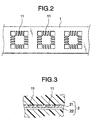
- Fig. 3 shows the contact interface between the mold and the leadframe.
- the stitches 11 of the leadframe bite into the pressure-sensitive adhesive layer 21 of the pressure-sensitive adhesive tape 2 so that the pressure-sensitive adhesive layer 21 and the stitches 11 are co-planar.
- the pressure-sensitive adhesive layer 21 among the stitches adheres to the mold 4 and acts as a sealant to exhibit high encapsulating properties. Therefore, the encapsulating effect can be exerted by increasing the thickness of the pressure-sensitive adhesive layer 21. Where the encapsulating resin fills deep into the gaps between stitches 11, a sufficient encapsulating effect can be exhibited by increasing the mold pressure or adhesive strength. Such manipulations can be selected according to the end use.
- the pressure-sensitive adhesive tape shrinks during resin encapsulating because it is also heated by the heat of the mold. A fear is entertained that the thermal shrinkage of the pressure-sensitive adhesive tape may cause a shear stress in the interface between the leadframe with the adhesive tape and the mold, and a high shear stress would deteriorate the encapsulating properties due to the shearing strain.
- the pressure-sensitive adhesive tape used has a thermal shrinkage of not more than 3%, preferably 2% or less, still preferably 1% or less, on resin encapsulating, the above-described high encapsulating performance can be secured during the resin encapsulating.
- the contact interface between the mold and the leadframe is made smaller, sufficient encapsulating can be achieved.
- the number of cavities per mold can be increased so that the number of chips encapsulated per shot can be increased. Since the chips are fixed onto the pressure-sensitive adhesive layer, the chips can be stably maintained in their fixed state against the resin flow thereby preventing breakage of the bonding parts.
- the pressure-sensitive adhesive strength of the pressure-sensitive adhesive tape is desirably as high as possible for encapsulating the contact between the mold and the leadframe but is desirably as low as possible for strippability from the leadframe after resin encapsulating. It is preferred to use a pressure-sensitive adhesive tape having a pressure-sensitive adhesive strength to the leadframe of 400 gf/20 mm or less, preferably 300 gf/20 mm or less and 5 gf/20 or more, at 23°C. If the pressure-sensitive adhesive strength is less than 5 gf/20 mm, the pressure-sensitive adhesive tape tends to separate during use.
- the heating conditions for resin encapsulating is usually about 180°C. It is a matter of course that the pressure-sensitive adhesive tape is required to have heat resistance to the heating temperature.
- the substrate of the pressure-sensitive adhesive tape can be of heat-resistant materials satisfying the above-described various conditions, for example, heat-resistant plastic films of polyimide, polyphenylene sulfide, etc., glass cloth, and the like. Where the heating condition of the resin encapsulating is 150°C or lower, a polyethylene terephthalate film may be used.
- the pressure-sensitive adhesives of the pressure-sensitive adhesive tape include not only acrylic pressure-sensititive adhesives and silicone pressure-sensitive adhesives but also epoxy adhesives as far as the above-described various conditions are met. It is preferred to use silicone pressure-sensitive adhesives having excellent heat resistance. In order to satisfy the above-specified requirement in terms of peel strength, heat-resistant fillers (such as glass beads, various inorganic fillers, arid heat-resistant organic fillers) can be added to the pressure-sensitive adhesive if desired. It is also possible to use a foaming adhesive which foams by the heat of resin encapsulating to reduce the peel strength to 400 gf/20 mm-tape width or less.
- the thickness of the substrate is from 5 to 250 ⁇ m, preferably 5 to 100 ⁇ m. If the thickness is smaller than 5 ⁇ m, the adhesive tape tends to be fractured, torn, or blistered, causing reduction of workability. If it exceeds 250 ⁇ m, the heat conduction efficiency from the mold to the resin is reduced.
- the thickness of the pressure-sensitive adhesive layer is from 2 to 100 ⁇ m, preferably 5 to 75 ⁇ m. If the thickness is less than 2 ⁇ m, there is a difficulty in coating, and an adhesive failure or blisters are liable to be caused. If it exceeds 100 ⁇ m, there is a difficulty in coating, and the adhesive tends to be pressed out from the edges, which attracts foreign matter and gives off increased gas on heating.
- the pressure-sensitive adhesive layer can be crosslinked appropriately in order that it can be stripped by interfacial separation without leaving any adhesive due to cohesive failure or in order to control the adhesive strength.
- the substrate can be subjected, if desired, to primer coating or surface roughening, for example, sputter etching.
- heat conductive particles such as boron nitride, can be added to the pressure-sensitive adhesive layer.
- the substrate can be of an electrically conductive material
- the pressure-sensitive adhesive layer can be made electrically conductive by addition of conductive particles, such as carbonickel or carbon black.
- the present invention is applicable to a TAB system.
- the pressure-sensitive adhesive tape is stuck to the back side of a film carrier tape (e.g., a polyimide film having copper foil finger leads), and semiconductor chips are disposed and fixed one by one in the device holes of the carrier tape with the pressure-sensitive adhesive tape.
- a film carrier tape e.g., a polyimide film having copper foil finger leads
- semiconductor chips are disposed and fixed one by one in the device holes of the carrier tape with the pressure-sensitive adhesive tape.
- Each of the chips and the finger leads of the film carrier tape are connected by Au-Sn eutectic bonding.
- the semiconductor chips are put in the respective cavities of a mold and encapsulated with a resin by transfer injection molding.
- the film carrier tape is then trimmed to obtain resin-encapsulated semiconductor chips.
- Chips bonded to a leadframe (Cu-based; number of stitches: 100) having no pressure-sensitive adhesive tape were put in a mold and encapsulated with a resin at 200°C and 20 kg/cm 2 . As a result, resin leaks occurred.
- a platinum catalyst (0.5 part by weight) was uniformly mixed into 100 parts by weight of a silicone pressure-sensitive adhesive. The mixture was applied to a 25 ⁇ m thick polyimide film and dried by heating at 130°C for 5 minutes to prepare a pressure-sensitive adhesive tape having a pressure-sensitive adhesive layer of 10 ⁇ m in thickness.
- the pressure-sensitive adhesive tape had a thermal shrinkage of 0.5% or less at 200°C and, when adhered to a leadframe, showed an initial pressure-sensitive adhesive strength of 60 gf/20 mm at 23°C, a pressure-sensitive adhesive strength of 180 gf/20 mm after 200°C x 1 hour, and a pressure-sensitive adhesive strength of 200 gf/20 mm after 200°C x 5 hours.
- the thermal shrinkage was determined by allowing a 300 mm long and 19 mm wide tape sample marked with two gauges at a distance of 200 mm to stand at 200°C for 2 hours and, after allowing the sample to cool to 23°C, measuring the distance between the two gauge marks.
- the thermal shrinkage was obtained as [(distance between two gauge marks before shrinkage - distance between two gauge marks after shrinkage)/distance between two gauge marks before shrinkage] x 100 (%) .
- the pressure-sensitive adhesive tape was stuck to the same leadframe as used in Comparative Example 1, and resin encapsulating was carried out in the same manner as in Comparative Example 1. The pressure-sensitive adhesive tape was then peeled. No resin leak nor deformation of the leadframe was observed.
- Resin encapsulating was carried out in the same manner as in Example 1, except for using an available silicone pressure-sensitive adhesive tape (pressure-sensitive adhesive layer thickness: 30 ⁇ m; substrate thickness: 25 ⁇ m) which has a thermal shrinkage of 0.5% or less at 200°C and, when adhered to a leadframe, shows an initial pressure-sensitive adhesive strength of 500 gf/20 mm at 23°C, a pressure-sensitive adhesive strength of 550 gf/20 mm after 200°C x 1 hour, and a pressure-sensitive adhesive strength of 550 gf/20 mm after 200°C x 5 hours. Because of the higher pressure-sensitive adhesive strength of the pressure-sensitive adhesive tape than that of Example 1, the leadframe was slightly deformed on peeling the adhesive tape, but no resin leak occurred.
- silicone pressure-sensitive adhesive tape pressure-sensitive adhesive layer thickness: 30 ⁇ m; substrate thickness: 25 ⁇ m
- This Example lends confirmation to the advantage of using a pressure-sensitive adhesive tape having an adhesive strength of 400 gf/20 mm or less after resin encapsulating.
- Resin encapsulating was carried out in the same manner as in Example 1, except for using a silicone pressure-sensitive adhesive tape (pressure-sensitive adhesive layer thickness: 10 ⁇ m; substrate thickness: 25 ⁇ m) which had a thermal shrinkage of 2% or less at 200°C and, when adhered to a leadframe, shows an initial pressure-sensitive adhesive strength of 220 gf/20 mm at 23°C, a pressure-sensitive adhesive strength of 300 gf/20 mm after 200°C x 1 hour, and a pressure-sensitive adhesive strength of 300 gf/20 mm after 200°C x 5 hours.
- a silicone pressure-sensitive adhesive tape pressure-sensitive adhesive layer thickness: 10 ⁇ m; substrate thickness: 25 ⁇ m
- Resin encapsulating was carried out in the same manner as in Example 1, except for using an available silicone pressure-sensitive adhesive tape (pressure-sensitive adhesive layer thickness: 30 ⁇ m; substrate thickness: 25 ⁇ m) which has a thermal shrinkage of 7.5% at 200°C and, when adhered to a leadframe, shows an initial pressure-sensitive adhesive strength of 700 gf/20 mm at 23°C, a pressure-sensitive adhesive strength of 750 gf/20 mm after 200°C x 1 hour, and a pressure-sensitive adhesive strength of 750 gf/20 mm after 200°C x 5 hours.
- an available silicone pressure-sensitive adhesive tape pressure-sensitive adhesive layer thickness: 30 ⁇ m; substrate thickness: 25 ⁇ m
- Resin encapsulating was carried out in the same manner as in Example 1, except for using an available silicone pressure-sensitive adhesive tape (pressure-sensitive adhesive layer thickness: 30 ⁇ m; substrate thickness: 25 ⁇ m) which has a thermal shrinkage of 7.5% at 200°C and, when adhered to a leadframe, shows an initial
- the present invention makes it feasible to sufficiently reduce the area of the contact interface between the leadframe, etc. and the mold. As a result, the number of cavities per mold can be increased so that the number of chips encapsulated in a single shot can be increased, leading to improved efficiency in resin encapsulating.
- the present invention satisfactorily prevents breakage of bonding parts during resin encapsulating, providing an excellent yield in resin encapsulating.
- the present invention prevents foreign matter's entering the stitches of a leadframe, development of scratches, dusting due to resin leaks, and so forth, leading to improved resin encapsulating quality.
Landscapes
- Encapsulation Of And Coatings For Semiconductor Or Solid State Devices (AREA)
- Structures Or Materials For Encapsulating Or Coating Semiconductor Devices Or Solid State Devices (AREA)
- Lead Frames For Integrated Circuits (AREA)
Applications Claiming Priority (3)
| Application Number | Priority Date | Filing Date | Title |
|---|---|---|---|
| JP11103559A JP2000294580A (ja) | 1999-04-12 | 1999-04-12 | 半導体チップの樹脂封止方法及びリ−ドフレ−ム等貼着用粘着テ−プ |
| JP10355999 | 1999-04-12 | ||
| PCT/JP1999/007387 WO2000062338A1 (en) | 1999-04-12 | 1999-12-28 | Semiconductor chip resin-sealing method and adhesive tape for pasting lead frames or the like |
Publications (2)
| Publication Number | Publication Date |
|---|---|
| EP1094512A1 true EP1094512A1 (de) | 2001-04-25 |
| EP1094512A4 EP1094512A4 (de) | 2006-05-17 |
Family
ID=14357182
Family Applications (1)
| Application Number | Title | Priority Date | Filing Date |
|---|---|---|---|
| EP99961462A Withdrawn EP1094512A4 (de) | 1999-04-12 | 1999-12-28 | Kunststoffeinkapselungsverfahren für halbleiterchip und klebeband zum kleben von leiterrahmen oder ähnlichem |
Country Status (6)
| Country | Link |
|---|---|
| EP (1) | EP1094512A4 (de) |
| JP (1) | JP2000294580A (de) |
| KR (1) | KR100665441B1 (de) |
| MY (1) | MY135733A (de) |
| TW (1) | TW464991B (de) |
| WO (1) | WO2000062338A1 (de) |
Cited By (5)
| Publication number | Priority date | Publication date | Assignee | Title |
|---|---|---|---|---|
| EP1261031A3 (de) * | 2001-05-18 | 2004-06-02 | Lintec Corporation | Trägerband für eine Verwendung als Harzträgersteg eines Leiterrahmens |
| EP1492164A4 (de) * | 2002-03-29 | 2007-10-31 | Matsushita Electric Industrial Co Ltd | Verfahren zur herstellung eines wärmeleitenden substrats |
| EP1887061A3 (de) * | 2006-08-10 | 2011-01-19 | Nitto Denko Corporation | Druckempfindliche Klebeblätter zum Schleifen eines Wafers |
| EP3040390A4 (de) * | 2013-08-29 | 2017-04-26 | Mitsui Chemicals Tohcello, Inc. | Haftfilm und verfahren zur herstellung eines halbleiterbauelements |
| CN108831839A (zh) * | 2018-06-22 | 2018-11-16 | 苏州震坤科技有限公司 | 一种去除半导体塑封制程中所产生毛边的方法 |
Families Citing this family (14)
| Publication number | Priority date | Publication date | Assignee | Title |
|---|---|---|---|---|
| JP4703842B2 (ja) * | 2000-11-30 | 2011-06-15 | 日東電工株式会社 | 堰材、及びこの堰材を用いた封止電子部品の製造方法 |
| KR100709007B1 (ko) * | 2001-04-13 | 2007-04-18 | 앰코 테크놀로지 코리아 주식회사 | 반도체 패키지 제조 방법 |
| US7061077B2 (en) | 2002-08-30 | 2006-06-13 | Fairchild Semiconductor Corporation | Substrate based unmolded package including lead frame structure and semiconductor die |
| CN1698200A (zh) | 2003-02-19 | 2005-11-16 | 日立化成工业株式会社 | 半导体用粘着薄膜 ,使用该粘着薄膜的附有粘着薄膜金属板 ,附有该粘着薄膜的配线电路及半导体装置 ,以及半导体装置的制造方法 |
| JP4125668B2 (ja) | 2003-12-19 | 2008-07-30 | 日東電工株式会社 | 半導体装置の製造方法 |
| JP2005252142A (ja) * | 2004-03-08 | 2005-09-15 | Shin Etsu Polymer Co Ltd | 薄型基板用固定治具 |
| KR100635053B1 (ko) | 2005-06-21 | 2006-10-16 | 도레이새한 주식회사 | 전자부품용 접착테이프 |
| WO2006114825A1 (ja) * | 2005-04-06 | 2006-11-02 | Renesas Technology Corp. | 半導体装置の製造方法 |
| JP2008207450A (ja) * | 2007-02-27 | 2008-09-11 | Towa Corp | 発光素子の圧縮成形方法 |
| JP5067927B2 (ja) * | 2007-03-27 | 2012-11-07 | 日東電工株式会社 | 半導体装置製造用接着フィルム |
| JP5125702B2 (ja) * | 2008-04-07 | 2013-01-23 | 株式会社デンソー | 電子装置の製造方法 |
| WO2012002446A1 (ja) * | 2010-07-02 | 2012-01-05 | 独立行政法人産業技術総合研究所 | 微小機械システム |
| CN103064248A (zh) * | 2011-10-21 | 2013-04-24 | 联胜(中国)科技有限公司 | 薄膜图案的制作方法及基板结构 |
| CN103305138A (zh) * | 2012-03-08 | 2013-09-18 | 日东电工株式会社 | 树脂密封用压敏粘合带和树脂密封型半导体器件的生产方法 |
Family Cites Families (6)
| Publication number | Priority date | Publication date | Assignee | Title |
|---|---|---|---|---|
| JPH0210748A (ja) * | 1988-06-29 | 1990-01-16 | Toshiba Corp | 電子部品の実装方法 |
| US5366809A (en) * | 1993-09-02 | 1994-11-22 | Dow Corning Corporation | Silicone pressure-sensitive adhesives |
| US5849397A (en) * | 1995-10-03 | 1998-12-15 | Ube Industries, Ltd. | Aromatic polyimide film and polyimide/copper foil composite sheet |
| JPH10189626A (ja) * | 1996-12-24 | 1998-07-21 | Nippon Retsuku Kk | 電子部品の製造方法 |
| JP2971834B2 (ja) * | 1997-06-27 | 1999-11-08 | 松下電子工業株式会社 | 樹脂封止型半導体装置の製造方法 |
| JP3729992B2 (ja) * | 1997-08-28 | 2005-12-21 | 株式会社ルネサステクノロジ | 半導体装置の製造方法およびそれに使用されるテープキャリア |
-
1999
- 1999-04-12 JP JP11103559A patent/JP2000294580A/ja active Pending
- 1999-12-28 WO PCT/JP1999/007387 patent/WO2000062338A1/ja not_active Ceased
- 1999-12-28 EP EP99961462A patent/EP1094512A4/de not_active Withdrawn
- 1999-12-28 KR KR1020007014112A patent/KR100665441B1/ko not_active Expired - Fee Related
-
2000
- 2000-04-11 MY MYPI20001524A patent/MY135733A/en unknown
- 2000-04-12 TW TW089106803A patent/TW464991B/zh not_active IP Right Cessation
Cited By (7)
| Publication number | Priority date | Publication date | Assignee | Title |
|---|---|---|---|---|
| EP1261031A3 (de) * | 2001-05-18 | 2004-06-02 | Lintec Corporation | Trägerband für eine Verwendung als Harzträgersteg eines Leiterrahmens |
| US6855418B2 (en) | 2001-05-18 | 2005-02-15 | Lintec Corporation | Tape for forming resin tie bar, resin tie bar, lead frame equipped with resin tie bar, resin-molded semiconductor device, and method for producing same |
| CN100350597C (zh) * | 2001-05-18 | 2007-11-21 | 琳得科株式会社 | 用于形成树脂拉杆的带和树脂拉杆 |
| EP1492164A4 (de) * | 2002-03-29 | 2007-10-31 | Matsushita Electric Industrial Co Ltd | Verfahren zur herstellung eines wärmeleitenden substrats |
| EP1887061A3 (de) * | 2006-08-10 | 2011-01-19 | Nitto Denko Corporation | Druckempfindliche Klebeblätter zum Schleifen eines Wafers |
| EP3040390A4 (de) * | 2013-08-29 | 2017-04-26 | Mitsui Chemicals Tohcello, Inc. | Haftfilm und verfahren zur herstellung eines halbleiterbauelements |
| CN108831839A (zh) * | 2018-06-22 | 2018-11-16 | 苏州震坤科技有限公司 | 一种去除半导体塑封制程中所产生毛边的方法 |
Also Published As
| Publication number | Publication date |
|---|---|
| TW464991B (en) | 2001-11-21 |
| MY135733A (en) | 2008-06-30 |
| WO2000062338A1 (en) | 2000-10-19 |
| KR20010052801A (ko) | 2001-06-25 |
| EP1094512A4 (de) | 2006-05-17 |
| KR100665441B1 (ko) | 2007-01-04 |
| JP2000294580A (ja) | 2000-10-20 |
Similar Documents
| Publication | Publication Date | Title |
|---|---|---|
| EP1094512A1 (de) | Kunststoffeinkapselungsverfahren für halbleiterchip und klebeband zum kleben von leiterrahmen oder ähnlichem | |
| JP5718005B2 (ja) | 半導体装置製造用耐熱性粘着テープ及びそのテープを用いた半導体装置の製造方法。 | |
| KR100618640B1 (ko) | 반도체 장치 제조용 접착시트와, 반도체 장치 및 그제조방법 | |
| KR102331226B1 (ko) | 다이싱용 점착 테이프 및 반도체 칩의 제조 방법 | |
| CN101617390A (zh) | 切割/芯片接合薄膜 | |
| CN102134453A (zh) | 无基板半导体封装制造用耐热性粘合片 | |
| JP4125668B2 (ja) | 半導体装置の製造方法 | |
| CN1469445A (zh) | 制作半导体器件和其中所用耐热压敏粘结带的方法 | |
| US20130244377A1 (en) | Heat-resistant pressure-sensitive adhesive tape for production of semiconductor device and method for producing semiconductor device using the tape | |
| JP5548077B2 (ja) | 樹脂封止用粘着テープ及び樹脂封止型半導体装置の製造方法 | |
| CN103305140A (zh) | 半导体器件生产用耐热性压敏粘合带和使用其生产半导体器件的方法 | |
| WO2012099159A1 (ja) | 半導体パッケージ製造工程用耐熱性粘着テープ | |
| JP2002275435A (ja) | 半導体装置組立用マスクシートおよび半導体装置の組み立て方法 | |
| EP2639278A1 (de) | Hitzebeständiges druckempfindliches Klebeband zur Herstellung eines Halbleiterbauelements und Verfahren zur Herstellung von Halbleiterbauelementen unter Verwendung des Klebebandes | |
| JP2000349107A (ja) | 半導体封止チップモジュールの製造方法及びその固定シート | |
| JP2002338910A (ja) | 半導体装置製造用粘着シート | |
| KR20200118811A (ko) | 반도체 장치 제조용 접착 시트 및 그것을 이용한 반도체 장치의 제조 방법 | |
| JP3779601B2 (ja) | 半導体装置組立用マスクシート | |
| EP2639277A1 (de) | Hitzebeständiges druckempfindliches Klebeband zur Herstellung eines Halbleiterbauelements und Verfahren zur Herstellung von Halbleiterbauelementen unter Verwendung des Klebebandes | |
| HK1035070A (en) | Semiconductor chip resin-sealing method and adhesive tape for pasting lead frames of the like | |
| JP2000256628A (ja) | 接着材フィルム、半導体搭載用外部接続用部材、半導体装置及びそれらの製造法 | |
| CN103305139A (zh) | 半导体器件生产用耐热性压敏粘合带以及使用其生产半导体器件的方法 | |
| JP2003147323A (ja) | 接着剤組成物、接着フィルム、半導体支持部材、半導体装置およびその製造方法 | |
| JP2006318999A (ja) | 半導体装置製造用接着フィルム | |
| WO2002075809A1 (en) | Mask sheet for assembling semiconductor device and method for assembling semiconductor device |
Legal Events
| Date | Code | Title | Description |
|---|---|---|---|
| PUAI | Public reference made under article 153(3) epc to a published international application that has entered the european phase |
Free format text: ORIGINAL CODE: 0009012 |
|
| 17P | Request for examination filed |
Effective date: 20001211 |
|
| AK | Designated contracting states |
Kind code of ref document: A1 Designated state(s): AT BE CH CY DE DK ES FI FR GB GR IE IT LI LU MC NL PT SE |
|
| A4 | Supplementary search report drawn up and despatched |
Effective date: 20060405 |
|
| RIC1 | Information provided on ipc code assigned before grant |
Ipc: C09J 183/04 20060101ALI20060330BHEP Ipc: H01L 21/56 20060101AFI20001023BHEP |
|
| 17Q | First examination report despatched |
Effective date: 20060810 |
|
| STAA | Information on the status of an ep patent application or granted ep patent |
Free format text: STATUS: THE APPLICATION IS DEEMED TO BE WITHDRAWN |
|
| 18D | Application deemed to be withdrawn |
Effective date: 20061219 |
|
| REG | Reference to a national code |
Ref country code: HK Ref legal event code: WD Ref document number: 1035070 Country of ref document: HK |