EP1096548A2 - Dispositif de traitement de plaquettes semiconductrices comprenant un détecteur de présence de plaquette et procédé - Google Patents
Dispositif de traitement de plaquettes semiconductrices comprenant un détecteur de présence de plaquette et procédé Download PDFInfo
- Publication number
- EP1096548A2 EP1096548A2 EP00309089A EP00309089A EP1096548A2 EP 1096548 A2 EP1096548 A2 EP 1096548A2 EP 00309089 A EP00309089 A EP 00309089A EP 00309089 A EP00309089 A EP 00309089A EP 1096548 A2 EP1096548 A2 EP 1096548A2
- Authority
- EP
- European Patent Office
- Prior art keywords
- wafer
- cooling chamber
- chamber
- processing
- sensor
- Prior art date
- Legal status (The legal status is an assumption and is not a legal conclusion. Google has not performed a legal analysis and makes no representation as to the accuracy of the status listed.)
- Withdrawn
Links
Images


Classifications
-
- H—ELECTRICITY
- H10—SEMICONDUCTOR DEVICES; ELECTRIC SOLID-STATE DEVICES NOT OTHERWISE PROVIDED FOR
- H10P—GENERIC PROCESSES OR APPARATUS FOR THE MANUFACTURE OR TREATMENT OF DEVICES COVERED BY CLASS H10
- H10P72/00—Handling or holding of wafers, substrates or devices during manufacture or treatment thereof
- H10P72/04—Apparatus for manufacture or treatment
- H10P72/0451—Apparatus for manufacturing or treating in a plurality of work-stations
- H10P72/0452—Apparatus for manufacturing or treating in a plurality of work-stations characterised by the layout of the process chambers
- H10P72/0454—Apparatus for manufacturing or treating in a plurality of work-stations characterised by the layout of the process chambers surrounding a central transfer chamber
-
- H—ELECTRICITY
- H10—SEMICONDUCTOR DEVICES; ELECTRIC SOLID-STATE DEVICES NOT OTHERWISE PROVIDED FOR
- H10P—GENERIC PROCESSES OR APPARATUS FOR THE MANUFACTURE OR TREATMENT OF DEVICES COVERED BY CLASS H10
- H10P72/00—Handling or holding of wafers, substrates or devices during manufacture or treatment thereof
- H10P72/06—Apparatus for monitoring, sorting, marking, testing or measuring
- H10P72/0606—Position monitoring, e.g. misposition detection or presence detection
Definitions
- the present invention relates to the field of semiconductor fabrication and, more particularly, to a semiconductor wafer processing apparatus having a wafer presence detector.
- Chip production involves many steps of semiconductor wafer processing, including several steps in which metals are deposited onto the wafers in vacuum deposition chambers.
- Multiple chamber semiconductor wafer processing machines are in use in the industry for various processing steps in the fabrication of semiconductors. These machines may include several evacuable chambers, including processing chambers, transfer chambers, and loadlock chambers. The machines may perform several processes simultaneously on different wafers or sequentially on the same wafer.
- Such an apparatus as disclosed, for example, in U.S. Patent No. 5,882,165 to Maydan et al ., generally includes a mechanical transfer arm positioned in a transfer chamber for moving a wafer sequentially through several processing modules. At times, however, the transfer arm may fail to pick up the wafer to be transferred, or the wafer breaks during the transfer. Unfortunately, such accidental events may go undetected until the processing cycle is completed and an operator unloads wafers from the machine. Failure to notice a missing or broken wafer potentially results in contamination of an entire lot of wafers as they continue to be processed through the apparatus.
- the present invention advantageously provides a semiconductor wafer processing apparatus which can detect wafer status in the cooling chamber.
- an apparatus preferably comprising an optical sensor positioned adjacent the cooling chamber window and directed toward the wafer support for sensing wafer status.
- the apparatus also preferably includes a wafer processing chamber, a wafer transfer module positioned adjacent the processing chamber, a wafer cooling chamber having a window and a wafer support therein.
- the wafer cooling chamber is adjacent the wafer transfer module for receiving and cooling wafers downstream from the processing chamber.
- the optical sensor preferably includes an optical source and optical receiver.
- An aspect of the invention includes a method for semiconductor processing in a semiconductor wafer processing apparatus comprising at least one wafer processing chamber, a wafer transfer module positioned adjacent the at least one processing chamber, and a wafer cooling chamber adjacent the wafer transfer module.
- the method preferably comprises the steps of processing a wafer in the processing chamber, transferring the wafer from the processing chamber to the cooling chamber using the transfer module, and providing and using a sensor associated with the wafer cooling chamber for sensing wafer status in the cooling chamber.
- the apparatus 5 comprises at least one wafer processing chamber 21 , and five such chambers 21 , 23 , 25 , 27 and 29 in the illustrated embodiment
- the processing chambers may be for the deposition of materials, such as metals, as will be readily understood by those skilled in the art.
- a wafer transfer module 19 is positioned adjacent the processing chambers for transferring wafers from one chamber to another.
- the further operation of the wafer transfer module 19 will also be readily understood by those skilled in the art and requires no further discussion herein.
- a wafer cooling chamber 17 is positioned adjacent the wafer transfer module 19 for receiving and cooling wafers downstream from the processing chambers 29 .
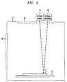
- the wafer cooling chamber 17 comprises a wafer support 31 and a window 33 adjacent the wafer support and in spaced apart relation therefrom.
- an optical sensor 35 is positioned adjacent the window 33 on the outside thereof, and is directed toward the wafer support 31 for sensing wafer 7 status.
- the sensor 35 is preferably positioned to sense wafer 7 status through the window 33 , wherein the wafer status includes at least one of presence, absence and breakage of the wafer 7 within the cooling chamber 17 .
- the optical sensor 35 preferably generates a signal responsive to wafer status.
- the apparatus 5 includes a controller 37 for controlling operation of the apparatus 5 . Accordingly, the optical sensor 35 is connected to the controller 37 for interrupting operation responsive to the wafer status signal.
- the cooling chamber 17 preferably also includes a cooling gas inlet port 39 for admitting cooling gas to cool the wafer 7 .
- the apparatus further comprises at least one load lock chamber 11 downstream from the cooling chamber 17 .
- Loadlock chambers 11 may function as both wafer inlet and wafer outlet chambers for the apparatus, as will be readily appreciated by those skilled in the art.
- Chamber 13 is also a wafer transfer chamber associated with the loadlock chambers 11 .
- the processing chambers are arranged about a portion of an imaginary circle so that a wafer 7 may be transferred from one chamber to another sequentially by the transfer module 19 for processing, such as cleaning or metal deposition, and finally transferred for cooling in the cooling chamber 17 .
- the optical sensor 35 preferably includes an optical source 41 and an optical receiver 43 cooperating therewith for sensing wafer 7 status.
- the optical sensor 35 may also include a plurality of optical sources and optical receivers cooperating to sense wafer status. Such a plurality of optical sources and optical receivers would be particularly useful in sensing a greater area of the wafer 7 to improve detection of breakage.
- the optical sensor 35 may also be positioned within the cooling chamber 17 itself.
- the cooling chamber 17 also further comprises an access port 45 for allowing operator access to the chamber. Skilled artisans will appreciate that such an access port may be positioned on the cooling chamber as practicable.
- Another aspect of the invention is directed to a method for semiconductor processing in a semiconductor wafer processing apparatus comprising at least one wafer processing chamber, a wafer transfer module positioned adjacent the at least one processing chamber, and a wafer cooling chamber adjacent the wafer transfer module.
- the method starts (Block 50) by the step of processing a wafer in the processing chamber (Block 52), transferring the wafer from the processing chamber to the cooling chamber (Block 54) using the transfer module, and providing and using a sensor associated with the wafer cooling chamber for sensing wafer status in the cooling chamber (Block 56).
- wafer status monitored includes at least one of presence or absence of the wafer (Block 58), and breakage of the wafer (Block 60) within said cooling chamber. Responsive to the sensing step, the sensor generates a wafer status signal. If the sensing step indicates a missing wafer, or a broken wafer (Block 63), the appropriate trouble signal is generated, operation is interrupted (Block 65), and the method stops (Block 66). If the sensing step indicates a wafer is present and unbroken, the appropriate signal is generated (Block 62), and processing continues until finished (Block 64), whereupon the method stops (Block 66).
Landscapes
- Chemical Vapour Deposition (AREA)
- Container, Conveyance, Adherence, Positioning, Of Wafer (AREA)
Applications Claiming Priority (2)
| Application Number | Priority Date | Filing Date | Title |
|---|---|---|---|
| US430768 | 1995-04-27 | ||
| US43076899A | 1999-10-29 | 1999-10-29 |
Publications (1)
| Publication Number | Publication Date |
|---|---|
| EP1096548A2 true EP1096548A2 (fr) | 2001-05-02 |
Family
ID=23708946
Family Applications (1)
| Application Number | Title | Priority Date | Filing Date |
|---|---|---|---|
| EP00309089A Withdrawn EP1096548A2 (fr) | 1999-10-29 | 2000-10-16 | Dispositif de traitement de plaquettes semiconductrices comprenant un détecteur de présence de plaquette et procédé |
Country Status (1)
| Country | Link |
|---|---|
| EP (1) | EP1096548A2 (fr) |
Cited By (3)
| Publication number | Priority date | Publication date | Assignee | Title |
|---|---|---|---|---|
| KR100454393B1 (ko) * | 2001-12-18 | 2004-10-26 | 코스텍시스템(주) | 복층 수직형 매엽식 반도체 웨이퍼 처리장치 |
| TWI549218B (zh) * | 2015-02-17 | 2016-09-11 | 力鼎精密股份有限公司 | 半導體設備及其處理腔室與被處理體搬運方法 |
| CN112233992A (zh) * | 2020-09-10 | 2021-01-15 | 上海华力集成电路制造有限公司 | 晶圆破片检测装置及其使用方法 |
-
2000
- 2000-10-16 EP EP00309089A patent/EP1096548A2/fr not_active Withdrawn
Cited By (3)
| Publication number | Priority date | Publication date | Assignee | Title |
|---|---|---|---|---|
| KR100454393B1 (ko) * | 2001-12-18 | 2004-10-26 | 코스텍시스템(주) | 복층 수직형 매엽식 반도체 웨이퍼 처리장치 |
| TWI549218B (zh) * | 2015-02-17 | 2016-09-11 | 力鼎精密股份有限公司 | 半導體設備及其處理腔室與被處理體搬運方法 |
| CN112233992A (zh) * | 2020-09-10 | 2021-01-15 | 上海华力集成电路制造有限公司 | 晶圆破片检测装置及其使用方法 |
Similar Documents
| Publication | Publication Date | Title |
|---|---|---|
| US8588950B2 (en) | Substrate processing apparatus | |
| US5886896A (en) | Method and apparatus for integrated control of a sensor in a manufacturing processing station | |
| US20010012392A1 (en) | Method and apparatus for inspecting wafers | |
| US20120226475A1 (en) | Substrate processing system, management apparatus, data analysis method | |
| US8126588B2 (en) | Method and system for controlling transport sequencing in a process tool by a look-ahead mode | |
| CN110858555B (zh) | 基板搬送模块和基板搬送方法 | |
| JP2014060412A (ja) | 半導体製造装置 | |
| US20050021272A1 (en) | Method and apparatus for performing metrology dispatching based upon fault detection | |
| JP4068404B2 (ja) | 基板処理システム、基板処理装置、基板処理方法、プログラム及び記録媒体 | |
| TW202209535A (zh) | 晶圓盒裝置、半導體處理機台和晶圓檢測方法 | |
| US7130762B2 (en) | Method and system for handling substrates in a production line including a cluster tool and a metrology tool | |
| EP1082755A1 (fr) | Poste tampon pour plaquettes et procede de transfert plaquette par plaquette entre des postes d'usinage | |
| EP1096548A2 (fr) | Dispositif de traitement de plaquettes semiconductrices comprenant un détecteur de présence de plaquette et procédé | |
| JPH085542A (ja) | 半導体装置の製造方法および装置 | |
| JP2005286102A (ja) | 真空処理装置および真空処理方法 | |
| JP4302491B2 (ja) | 枚葉式真空処理装置 | |
| EP1098351A2 (fr) | Dispositif et méthode de détection de défauts d'alignement des plaquettes semiconductrices dans une cassette | |
| US12224199B2 (en) | Semiconductor manufacturing apparatus and method for manufacturing semiconductor device | |
| US7184851B2 (en) | Method of providing cassettes containing control wafers to designated processing tools and metrology tools | |
| EP1747575B1 (fr) | Detection inter-processus pour le controle du resultat de la fabrication d'une plaquette | |
| US5604134A (en) | Particle monitoring method for plasma reactors with moving gas distribution housings | |
| KR20050045339A (ko) | 웨이퍼 이송장치 | |
| KR100495419B1 (ko) | 반도체제조장치 | |
| KR100689696B1 (ko) | 반도체장치 제조시스템 및 그 운영방법 | |
| KR20060084926A (ko) | 웨이퍼 가공 장치 |
Legal Events
| Date | Code | Title | Description |
|---|---|---|---|
| PUAI | Public reference made under article 153(3) epc to a published international application that has entered the european phase |
Free format text: ORIGINAL CODE: 0009012 |
|
| AK | Designated contracting states |
Kind code of ref document: A2 Designated state(s): AT BE CH CY DE DK ES FI FR GB GR IE IT LI LU MC NL PT SE |
|
| AX | Request for extension of the european patent |
Free format text: AL;LT;LV;MK;RO;SI |
|
| STAA | Information on the status of an ep patent application or granted ep patent |
Free format text: STATUS: THE APPLICATION HAS BEEN WITHDRAWN |
|
| 18W | Application withdrawn |
Withdrawal date: 20010717 |