EP1096567A2 - KMG und seine Herstellung - Google Patents
KMG und seine Herstellung Download PDFInfo
- Publication number
- EP1096567A2 EP1096567A2 EP00106301A EP00106301A EP1096567A2 EP 1096567 A2 EP1096567 A2 EP 1096567A2 EP 00106301 A EP00106301 A EP 00106301A EP 00106301 A EP00106301 A EP 00106301A EP 1096567 A2 EP1096567 A2 EP 1096567A2
- Authority
- EP
- European Patent Office
- Prior art keywords
- substrate
- semiconductor chip
- solder balls
- holes
- resin
- Prior art date
- Legal status (The legal status is an assumption and is not a legal conclusion. Google has not performed a legal analysis and makes no representation as to the accuracy of the status listed.)
- Withdrawn
Links
Images









Classifications
-
- H—ELECTRICITY
- H10—SEMICONDUCTOR DEVICES; ELECTRIC SOLID-STATE DEVICES NOT OTHERWISE PROVIDED FOR
- H10W—GENERIC PACKAGES, INTERCONNECTIONS, CONNECTORS OR OTHER CONSTRUCTIONAL DETAILS OF DEVICES COVERED BY CLASS H10
- H10W40/00—Arrangements for thermal protection or thermal control
- H10W40/10—Arrangements for heating
-
- H—ELECTRICITY
- H10—SEMICONDUCTOR DEVICES; ELECTRIC SOLID-STATE DEVICES NOT OTHERWISE PROVIDED FOR
- H10W—GENERIC PACKAGES, INTERCONNECTIONS, CONNECTORS OR OTHER CONSTRUCTIONAL DETAILS OF DEVICES COVERED BY CLASS H10
- H10W70/00—Package substrates; Interposers; Redistribution layers [RDL]
- H10W70/60—Insulating or insulated package substrates; Interposers; Redistribution layers
- H10W70/67—Insulating or insulated package substrates; Interposers; Redistribution layers characterised by their insulating layers or insulating parts
- H10W70/68—Shapes or dispositions thereof
-
- H—ELECTRICITY
- H10—SEMICONDUCTOR DEVICES; ELECTRIC SOLID-STATE DEVICES NOT OTHERWISE PROVIDED FOR
- H10W—GENERIC PACKAGES, INTERCONNECTIONS, CONNECTORS OR OTHER CONSTRUCTIONAL DETAILS OF DEVICES COVERED BY CLASS H10
- H10W72/00—Interconnections or connectors in packages
- H10W72/30—Die-attach connectors
-
- H—ELECTRICITY
- H10—SEMICONDUCTOR DEVICES; ELECTRIC SOLID-STATE DEVICES NOT OTHERWISE PROVIDED FOR
- H10W—GENERIC PACKAGES, INTERCONNECTIONS, CONNECTORS OR OTHER CONSTRUCTIONAL DETAILS OF DEVICES COVERED BY CLASS H10
- H10W76/00—Containers; Fillings or auxiliary members therefor; Seals
- H10W76/40—Fillings or auxiliary members in containers, e.g. centering rings
- H10W76/42—Fillings
- H10W76/47—Solid or gel fillings
-
- H—ELECTRICITY
- H10—SEMICONDUCTOR DEVICES; ELECTRIC SOLID-STATE DEVICES NOT OTHERWISE PROVIDED FOR
- H10W—GENERIC PACKAGES, INTERCONNECTIONS, CONNECTORS OR OTHER CONSTRUCTIONAL DETAILS OF DEVICES COVERED BY CLASS H10
- H10W90/00—Package configurations
-
- H—ELECTRICITY
- H10—SEMICONDUCTOR DEVICES; ELECTRIC SOLID-STATE DEVICES NOT OTHERWISE PROVIDED FOR
- H10W—GENERIC PACKAGES, INTERCONNECTIONS, CONNECTORS OR OTHER CONSTRUCTIONAL DETAILS OF DEVICES COVERED BY CLASS H10
- H10W90/00—Package configurations
- H10W90/701—Package configurations characterised by the relative positions of pads or connectors relative to package parts
-
- H—ELECTRICITY
- H10—SEMICONDUCTOR DEVICES; ELECTRIC SOLID-STATE DEVICES NOT OTHERWISE PROVIDED FOR
- H10W—GENERIC PACKAGES, INTERCONNECTIONS, CONNECTORS OR OTHER CONSTRUCTIONAL DETAILS OF DEVICES COVERED BY CLASS H10
- H10W70/00—Package substrates; Interposers; Redistribution layers [RDL]
- H10W70/60—Insulating or insulated package substrates; Interposers; Redistribution layers
- H10W70/62—Insulating or insulated package substrates; Interposers; Redistribution layers characterised by their interconnections
- H10W70/65—Shapes or dispositions of interconnections
- H10W70/654—Top-view layouts
- H10W70/655—Fan-out layouts
-
- H—ELECTRICITY
- H10—SEMICONDUCTOR DEVICES; ELECTRIC SOLID-STATE DEVICES NOT OTHERWISE PROVIDED FOR
- H10W—GENERIC PACKAGES, INTERCONNECTIONS, CONNECTORS OR OTHER CONSTRUCTIONAL DETAILS OF DEVICES COVERED BY CLASS H10
- H10W70/00—Package substrates; Interposers; Redistribution layers [RDL]
- H10W70/60—Insulating or insulated package substrates; Interposers; Redistribution layers
- H10W70/67—Insulating or insulated package substrates; Interposers; Redistribution layers characterised by their insulating layers or insulating parts
- H10W70/68—Shapes or dispositions thereof
- H10W70/681—Shapes or dispositions thereof comprising holes not having chips therein, e.g. for outgassing, underfilling or bond wire passage
-
- H—ELECTRICITY
- H10—SEMICONDUCTOR DEVICES; ELECTRIC SOLID-STATE DEVICES NOT OTHERWISE PROVIDED FOR
- H10W—GENERIC PACKAGES, INTERCONNECTIONS, CONNECTORS OR OTHER CONSTRUCTIONAL DETAILS OF DEVICES COVERED BY CLASS H10
- H10W70/00—Package substrates; Interposers; Redistribution layers [RDL]
- H10W70/60—Insulating or insulated package substrates; Interposers; Redistribution layers
- H10W70/67—Insulating or insulated package substrates; Interposers; Redistribution layers characterised by their insulating layers or insulating parts
- H10W70/68—Shapes or dispositions thereof
- H10W70/682—Shapes or dispositions thereof comprising holes having chips therein
-
- H—ELECTRICITY
- H10—SEMICONDUCTOR DEVICES; ELECTRIC SOLID-STATE DEVICES NOT OTHERWISE PROVIDED FOR
- H10W—GENERIC PACKAGES, INTERCONNECTIONS, CONNECTORS OR OTHER CONSTRUCTIONAL DETAILS OF DEVICES COVERED BY CLASS H10
- H10W70/00—Package substrates; Interposers; Redistribution layers [RDL]
- H10W70/60—Insulating or insulated package substrates; Interposers; Redistribution layers
- H10W70/67—Insulating or insulated package substrates; Interposers; Redistribution layers characterised by their insulating layers or insulating parts
- H10W70/68—Shapes or dispositions thereof
- H10W70/685—Shapes or dispositions thereof comprising multiple insulating layers
-
- H—ELECTRICITY
- H10—SEMICONDUCTOR DEVICES; ELECTRIC SOLID-STATE DEVICES NOT OTHERWISE PROVIDED FOR
- H10W—GENERIC PACKAGES, INTERCONNECTIONS, CONNECTORS OR OTHER CONSTRUCTIONAL DETAILS OF DEVICES COVERED BY CLASS H10
- H10W72/00—Interconnections or connectors in packages
- H10W72/071—Connecting or disconnecting
- H10W72/072—Connecting or disconnecting of bump connectors
-
- H—ELECTRICITY
- H10—SEMICONDUCTOR DEVICES; ELECTRIC SOLID-STATE DEVICES NOT OTHERWISE PROVIDED FOR
- H10W—GENERIC PACKAGES, INTERCONNECTIONS, CONNECTORS OR OTHER CONSTRUCTIONAL DETAILS OF DEVICES COVERED BY CLASS H10
- H10W72/00—Interconnections or connectors in packages
- H10W72/071—Connecting or disconnecting
- H10W72/073—Connecting or disconnecting of die-attach connectors
-
- H—ELECTRICITY
- H10—SEMICONDUCTOR DEVICES; ELECTRIC SOLID-STATE DEVICES NOT OTHERWISE PROVIDED FOR
- H10W—GENERIC PACKAGES, INTERCONNECTIONS, CONNECTORS OR OTHER CONSTRUCTIONAL DETAILS OF DEVICES COVERED BY CLASS H10
- H10W72/00—Interconnections or connectors in packages
- H10W72/071—Connecting or disconnecting
- H10W72/075—Connecting or disconnecting of bond wires
-
- H—ELECTRICITY
- H10—SEMICONDUCTOR DEVICES; ELECTRIC SOLID-STATE DEVICES NOT OTHERWISE PROVIDED FOR
- H10W—GENERIC PACKAGES, INTERCONNECTIONS, CONNECTORS OR OTHER CONSTRUCTIONAL DETAILS OF DEVICES COVERED BY CLASS H10
- H10W72/00—Interconnections or connectors in packages
- H10W72/851—Dispositions of multiple connectors or interconnections
- H10W72/874—On different surfaces
- H10W72/884—Die-attach connectors and bond wires
-
- H—ELECTRICITY
- H10—SEMICONDUCTOR DEVICES; ELECTRIC SOLID-STATE DEVICES NOT OTHERWISE PROVIDED FOR
- H10W—GENERIC PACKAGES, INTERCONNECTIONS, CONNECTORS OR OTHER CONSTRUCTIONAL DETAILS OF DEVICES COVERED BY CLASS H10
- H10W72/00—Interconnections or connectors in packages
- H10W72/90—Bond pads, in general
- H10W72/951—Materials of bond pads
-
- H—ELECTRICITY
- H10—SEMICONDUCTOR DEVICES; ELECTRIC SOLID-STATE DEVICES NOT OTHERWISE PROVIDED FOR
- H10W—GENERIC PACKAGES, INTERCONNECTIONS, CONNECTORS OR OTHER CONSTRUCTIONAL DETAILS OF DEVICES COVERED BY CLASS H10
- H10W72/00—Interconnections or connectors in packages
- H10W72/90—Bond pads, in general
- H10W72/951—Materials of bond pads
- H10W72/952—Materials of bond pads comprising metals or metalloids, e.g. PbSn, Ag or Cu
-
- H—ELECTRICITY
- H10—SEMICONDUCTOR DEVICES; ELECTRIC SOLID-STATE DEVICES NOT OTHERWISE PROVIDED FOR
- H10W—GENERIC PACKAGES, INTERCONNECTIONS, CONNECTORS OR OTHER CONSTRUCTIONAL DETAILS OF DEVICES COVERED BY CLASS H10
- H10W74/00—Encapsulations, e.g. protective coatings
-
- H—ELECTRICITY
- H10—SEMICONDUCTOR DEVICES; ELECTRIC SOLID-STATE DEVICES NOT OTHERWISE PROVIDED FOR
- H10W—GENERIC PACKAGES, INTERCONNECTIONS, CONNECTORS OR OTHER CONSTRUCTIONAL DETAILS OF DEVICES COVERED BY CLASS H10
- H10W74/00—Encapsulations, e.g. protective coatings
- H10W74/10—Encapsulations, e.g. protective coatings characterised by their shape or disposition
- H10W74/15—Encapsulations, e.g. protective coatings characterised by their shape or disposition on active surfaces of flip-chip devices, e.g. underfills
-
- H—ELECTRICITY
- H10—SEMICONDUCTOR DEVICES; ELECTRIC SOLID-STATE DEVICES NOT OTHERWISE PROVIDED FOR
- H10W—GENERIC PACKAGES, INTERCONNECTIONS, CONNECTORS OR OTHER CONSTRUCTIONAL DETAILS OF DEVICES COVERED BY CLASS H10
- H10W90/00—Package configurations
- H10W90/20—Configurations of stacked chips
- H10W90/291—Configurations of stacked chips characterised by containers, encapsulations, or other housings for the stacked chips
-
- H—ELECTRICITY
- H10—SEMICONDUCTOR DEVICES; ELECTRIC SOLID-STATE DEVICES NOT OTHERWISE PROVIDED FOR
- H10W—GENERIC PACKAGES, INTERCONNECTIONS, CONNECTORS OR OTHER CONSTRUCTIONAL DETAILS OF DEVICES COVERED BY CLASS H10
- H10W90/00—Package configurations
- H10W90/20—Configurations of stacked chips
- H10W90/297—Configurations of stacked chips characterised by the through-semiconductor vias [TSVs] in the stacked chips
-
- H—ELECTRICITY
- H10—SEMICONDUCTOR DEVICES; ELECTRIC SOLID-STATE DEVICES NOT OTHERWISE PROVIDED FOR
- H10W—GENERIC PACKAGES, INTERCONNECTIONS, CONNECTORS OR OTHER CONSTRUCTIONAL DETAILS OF DEVICES COVERED BY CLASS H10
- H10W90/00—Package configurations
- H10W90/701—Package configurations characterised by the relative positions of pads or connectors relative to package parts
- H10W90/721—Package configurations characterised by the relative positions of pads or connectors relative to package parts of bump connectors
- H10W90/724—Package configurations characterised by the relative positions of pads or connectors relative to package parts of bump connectors between a chip and a stacked insulating package substrate, interposer or RDL
-
- H—ELECTRICITY
- H10—SEMICONDUCTOR DEVICES; ELECTRIC SOLID-STATE DEVICES NOT OTHERWISE PROVIDED FOR
- H10W—GENERIC PACKAGES, INTERCONNECTIONS, CONNECTORS OR OTHER CONSTRUCTIONAL DETAILS OF DEVICES COVERED BY CLASS H10
- H10W90/00—Package configurations
- H10W90/701—Package configurations characterised by the relative positions of pads or connectors relative to package parts
- H10W90/731—Package configurations characterised by the relative positions of pads or connectors relative to package parts of die-attach connectors
- H10W90/734—Package configurations characterised by the relative positions of pads or connectors relative to package parts of die-attach connectors between a chip and a stacked insulating package substrate, interposer or RDL
-
- H—ELECTRICITY
- H10—SEMICONDUCTOR DEVICES; ELECTRIC SOLID-STATE DEVICES NOT OTHERWISE PROVIDED FOR
- H10W—GENERIC PACKAGES, INTERCONNECTIONS, CONNECTORS OR OTHER CONSTRUCTIONAL DETAILS OF DEVICES COVERED BY CLASS H10
- H10W90/00—Package configurations
- H10W90/701—Package configurations characterised by the relative positions of pads or connectors relative to package parts
- H10W90/751—Package configurations characterised by the relative positions of pads or connectors relative to package parts of bond wires
- H10W90/754—Package configurations characterised by the relative positions of pads or connectors relative to package parts of bond wires between a chip and a stacked insulating package substrate, interposer or RDL
Definitions
- the present invention relates to a BGA (Ball Grid Array) package, and a method for fabricating the same.
- BGA All Grid Array
- a conventional BGA package includes a substrate having a copper plate, an insulating layer and a copper wiring pattern.
- the BGA package is designed to have a good characteristic of heat radiation.
- the insulating layer may be of polyimide, which is formed on the copper plate.
- the copper wiring pattern is formed on the insulating layer.
- the substrate is provided with solder balls to be connected to a motherboard.
- a semiconductor chip is connected at electrodes to the copper wiring pattern by bonding wires.
- an object of the present invention is to provide a ball grid array (BGA) package in which solder balls are used efficiently without making a large number of excess terminals (solder balls). This feature allows that a BGA package can be fabricated small in size with higher integration.
- BGA ball grid array
- Another object of the present invention is to provide a method for fabricating a ball grid array (BGA) package in which solder balls are used efficiently without making a large number of excess terminals (solder balls). This feature allows that a BGA package can be fabricated small in size with higher integration.
- BGA ball grid array
- a ball grid array (BGA) package includes a substrate (20) having first and second surfaces, and through holes (30) passing through it.
- the package further includes a first semiconductor chip (28) which is mounted on the first surface of the substrate (20); a second semiconductor chip (36) which is mounted on the second surface of the substrate (20); and solder balls (34) which are provided on the first surface of the substrate (20) and are electrically connected to the first semiconductor chip (28).
- the second semiconductor chip (36) is electrically connected via the through holes (30) to the solder balls (34).
- a method includes the steps of providing a substrate (20) having first and second surfaces, and through holes (30) passing through it; mounting a first semiconductor chip (28) on the first surface of the substrate (20); and mounting a second semiconductor chip (36) on the second surface of the substrate (20).
- the method further includes the step of providing solder balls (34) on the first surface of the substrate (20) so that the solder balls (34) are electrically connected to the first semiconductor chip (28) and to the second semiconductor chip (36) via the through holes (30).
- Fig. 1 shows a conventional BGA package
- Fig. 2 shows a part encircled by a broken line "A" in Fig. 1.
- the BGA package includes a copper plate 1, an insulating layer 2 and a copper wiring pattern 3.
- the BGA package is designed to have a good characteristic of heat radiation.
- the copper plate 1 is shaped to have a thickness of 0.3 to 0.4mm.
- the insulating layer 2 may be of polyimide having a thickness of 10 to 30 ⁇ m, which is adhered onto the copper plate 1.
- the copper wiring pattern 3 is shaped to have a thickness of 12 to 35 ⁇ m and is formed on the insulating layer 2.
- the copper plate 1 is cut off to provide a cavity 5a in which a semiconductor chip 4 is placed.
- the semiconductor chip 4 has electrode side surface (front surface) and rear surface.
- the semiconductor chip 4 is fixed at the rear surface to the bottom of the cavity 5a with an insulating paste 6.
- the semiconductor chip 4 is connected at electrodes to the copper wiring pattern 3 by bonding wires 7.
- the cavity 5a is to be filled up with an epoxy resin 8.
- the substrate structure is provided at regions uncovered with the epoxy resin 8 with solder balls 9, which are arranged in lattice manner. The other regions of the substrate structure is covered with a resist layer 10.
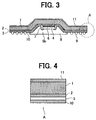
- Fig. 3 shows another conventional BGA package
- Fig. 4 shows a part encircled by a broken line "A" in Fig. 3.
- the BGA package includes a copper plate 1, an insulating layer 2 and a copper wiring pattern 3.
- a metal mold reduction (drawing) process is carried out to the copper plate 1 to form a cavity 5b in which a semiconductor chip 4 is placed.
- the copper plate 1 may be provided at the rear surface with another insulating layer 11 to reduce the degree of bending of the structure and to prevent contamination.
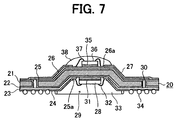
- Fig. 7 shows a BGA package according to a first preferred embodiment of the present invention.
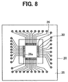
- Figs. 8 to 10 show a substrate (20) used for fabricating the BGA package, shown in Fig. 7.
- the BGA package includes a substrate 20, which includes a copper plate 21 shaped to have a thickness of 0.3 to 0.4mm.
- the copper plate 21 is provided on a front surface with an insulating layer 22 of polyimide having a thickness of 10 to 30 ⁇ m.
- a copper wiring pattern 23 is formed on the insulating layer 22.
- a solder resist 24 is formed (spread) over the copper wiring pattern 23 except some areas thereon.
- the copper plate 21 is provided on a rear surface with another insulating layer 25 of polyimide having a thickness of 10 to 30 ⁇ m.
- Another copper wiring pattern 26 is formed on the insulating layer 25 to have a thickness of 12 to 35 ⁇ m.
- Another solder resist 27 is formed (spread) over the copper wiring pattern 26 except some areas thereon.
- the substrate 20 includes the copper plate 21, insulating layers 22 and 25, copper wiring patterns 23 and 26.
- a metal mold reduction (drawing) process is carried out to the substrate 20 to form a cavity 29 at the front surface in which a semiconductor chip 28 is placed.
- the copper plate 21 is provided therein with through holes 30, which connect the front surface and rear surface thereof.
- the through holes 30 are insulated from the copper plate 21.
- One ends of the copper wiring patterns 23 and 26 form bonding posts 25a and 26a, which are to be connected to bonding wires 32 and 37.
- the other ends of the copper wiring pattern 26 are connected to the through holes 30.
- an insulating paste 31 is formed (spread) over so that the semiconductor chip 28 is well fixed at the rear surface in the cavity 29.
- the semiconductor chip 28 is provided at the rear surface with no electrodes.
- the semiconductor chip 28 is connected at the electrodes to the copper wiring pattern 23 by the bonding wires 32.
- the cavity 29 is to be filled up with an epoxy resin 33.
- the substrate 20 is provided at the front surface with solder balls 34, which are arranged in lattice manner.
- the solder balls 34 are arranged at exposed regions of the solder resist 27.
- Each of the through holes 30 is connected to the solder balls 34.
- Another insulating paste 35 is formed (spread) over a part of the rear surface of the substrate 20 so that another semiconductor chip 36 is mounted on the substrate 20.
- the semiconductor chip 36 is connected at electrodes to the bonding posts 26a of the copper wiring pattern 26 by the bonding wires 37.
- the semiconductor chip 36 is sealed with an epoxy resin 38 in the same manner as the semiconductor chip 28.
- electrical signals are transferred to/from the semiconductor chip 28 through the solder balls 34 and copper wiring pattern 23. Further, electrical signals are transferred to/from the other semiconductor chip 36 through the solder balls 34, through holes 30 and copper wiring pattern 26.
- the copper wiring patterns 23 and 26 are formed both on the front and rear surfaces of the copper plate 21; and the semiconductor chip 36 mounted on the rear surface of the base plate 21 is connected at its electrodes to the solder balls 34 arranged on the front surface of the base plate (21) via the through holes 30. Therefore, the excess terminals, which are the solder balls 34 not connected to the semiconductor chip 28, can be used as terminals to be connected to the other semiconductor chip 36.
- the semiconductor chips 28 and 36 are mounted on the both surface of the substrate, so that only a small area is need to mount two semiconductor chips on a motherboard. It means that the motherboard can be designed smaller in size.
- Fig. 11 shows a BGA package according to a second preferred embodiment of the present invention.
- Figs. 12 and 13 show a substrate (40) used for fabricating the BGA package, shown in Fig. 11.
- the BGA package includes a substrate 40, which includes a copper plate 41.
- the copper plate 41 is provided on a front surface with an insulating layer 42 of polyimide having a thickness of 10 to 30 ⁇ m.
- a copper wiring pattern 43 is formed on the insulating layer 42.
- a solder resist 44 is formed (spread) over the copper wiring pattern 43 except some areas thereon.
- the copper plate 41 is provided on a rear surface with another insulating layer 45 of polyimide having a thickness of 10 to 30 ⁇ m.
- Another copper wiring pattern 46 is formed on the insulating layer 45 to have a thickness of 12 to 35 ⁇ m.
- Another solder resist 47 is formed (spread) over the copper wiring pattern 46 except some areas thereon.
- the substrate 40 includes at least the copper plate 41, insulating layers 42 and 45, and copper wiring patterns 43 and 46.
- a metal mold reduction (drawing) process is carried out to the substrate 40 to form a cavity 49 at the front surface in which a semiconductor chip 48 is placed.
- the copper plate 41 is provided therein with through holes 50, which connect the front surface and rear surface thereof.
- the through holes 50 are insulated from the copper plate 41.
- One ends of the copper wiring pattern 43 form bonding posts 43a, which are to be connected to bonding wires 52.
- One ends of the copper wiring pattern 46 form lands 46a, which are to be connected to gold bumps 55.
- the lands 46a are formed by steps of plating Ni as a base and plating gold thereon.
- the other ends of the copper wiring pattern 46 are connected to the through holes 50.
- an insulating paste 51 is formed (spread) over so that the semiconductor chip 48 is well fixed at the rear surface in the cavity 49.
- the semiconductor chip 48 is provided at the rear surface with no electrodes.
- the semiconductor chip 48 is connected at the electrodes to the copper wiring pattern 43 by the bonding wires 52.
- the cavity 49 is to be filled up with an epoxy resin 53.
- the substrate 40 is provided at the front surface with solder balls 54, which are arranged in lattice manner.
- the solder balls 54 are arranged at exposed regions of the solder resist 47.
- Each of the through holes 50 is connected to the solder balls 54.
- Another semiconductor chip 56 is mounted on the rear surface of the substrate 40 so that an electrode side surface of the semiconductor chip 56 opposes to the rear surface of the substrate 40.
- the semiconductor chip 56 is provided at the electrode side surface with the gold bumps 55 so that the electrodes of the semiconductor chip 56 are electrically connected to the copper wiring pattern 46 through the gold bumps 55.
- a space formed between the rear surface of the substrate 40 and electrode side surface of the semiconductor chip 56 is filled up with a seal resin 57.
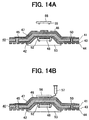
- Figs. 14A to 14D are cross-sectional views showing the fabrication steps of the BGA package, shown in Fig. 11.
- the through holes 50 are patterned in the copper plate 41; then the insulating layer 42 is adhered onto the front surface of the copper plate 41; and the copper wiring pattern 43 is formed on the insulating layer 42.
- the insulating layer 45 is adhered onto the rear surface of the copper plate 41, and the copper wiring pattern 46 is formed on the insulating layer 45.
- the solder resists 44 and 47 are provided on the copper wiring patterns 43 and 46, respectively, and then the semiconductor chip 48 is mounted in the cavity 49.
- the semiconductor chip 48 is connected at the electrodes to the copper wiring pattern 43 by the bonding wires 52.
- the semiconductor chip 48 is sealed with the epoxy resin 53.
- the gold bumps 55 are arranged on the electrodes of the semiconductor chip 56 so that the bumps 55 are projecting outwardly.
- the semiconductor chip 56 is positioned so that the electrode side surface thereof opposes to the rear surface of the substrate 40, and then the gold bumps 55 are in contact with the lands 46a of the substrate 40. After that, the resin 57 is injected sidewardly into the space between the semiconductor chip 56 and the substrate 40.
- the resin 57 is hardened with heat to seal the semiconductor chip 56 therein.
- the solder balls 64 are provided onto the front surface of the substrate 40.
- electrical signals are transferred to/from the semiconductor chip 48 through the solder balls 54 and copper wiring pattern 43. Further, electrical signals are transferred to/from the other semiconductor chip 54 through the solder balls 54, through holes 50 and copper wiring pattern 46.
- the excess terminals which are the solder balls 54 not connected to the semiconductor chip 48, can be used as terminals to be connected to the other semiconductor chip 56, in the same manner as the first preferred embodiment.
- the semiconductor chips 48 and 56 are mounted on the both surface of the substrate 40, so that only a small area is needed to mount two semiconductor chips on a motherboard. It means that the motherboard can be designed smaller in size.
- the semiconductor chip 56 is mounted on the substrate 40 using the gold bumps 56, so that the BGA package can be fabricated in a shorter period of time as compared to the first preferred embodiment.
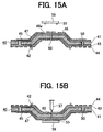
- Figs. 15A to 15E are cross-sectional views showing the fabrication steps of a BGA package, according to a third preferred embodiment of the present invention.
- the same or corresponding elements to those in the second preferred embodiment are represented by the same reference numerals and the same description is not repeated for avoiding redundant explanation.
- a patterning process is carried out to form an insulating layer 42 on a front surface of a copper plate 41, and then a copper wiring pattern 43 is formed on the insulating layer 42.
- Another insulating layer 45 is formed on the rear surface of the copper plate 41, and then another copper wiring pattern 46 is formed on the insulating layer 45.
- through holes 50 are formed in the copper plate 41.
- solder resists 44 and 47 are formed on the copper wiring patterns 43 and 46.
- a hole 60 is formed in the substrate 40 at the center of a region where a semiconductor chip 56 is to be mounted. The hole 60 passes through the substrate 40.
- Gold bumps 55 are arranged on electrodes of the semiconductor chip 56 so that the bumps 55 are projecting outwardly.
- the semiconductor chip 56 is positioned so that the electrode side surface opposes to the rear surface of the substrate 40, and then the gold bumps 55 are in contact with the lands 46a of the substrate 40.
- the gold bumps 55 are heated and pressed to the lands 46a so that those are connected to each other.
- resin 57 is injected into the space between the semiconductor chip 56 and the substrate 40 through the hole 60.
- the resin 57 is hardened with heat to seal the semiconductor chip 56 therein.
- the semiconductor chip 48 is mounted onto the cavity 49, and then the electrodes thereof are connected to the copper wiring pattern 43 by the bonding wires 52.
- the electrode side surface of the semiconductor chip 48 is sealed with an epoxy resin 53.
- the solder balls 64 are provided onto the front surface of the substrate 40.
- the excess terminals which are the solder balls 54 not connected to the semiconductor chip 48, can be used as terminals to be connected to the other semiconductor chip 56.
- the semiconductor chips 48 and 56 are mounted on the both surface of the substrate 40, so that only a small area is needed to mount two semiconductor chips on a motherboard. It means that the motherboard can be designed smaller in size.
- the semiconductor chip 56 is mounted on the substrate 40 using the gold bumps 56, so that the BGA package can be fabricated in a shorter period of time as compared to the first preferred embodiment. Further more, the resin 57 is supplied through the hole 60, passing through the substrate 40, the resin 57 can be spread uniformly. As a result, the resin 57 keeps its original shape even after the package is completed; and the semiconductor chip 56 may keep its reliability of connection (operation) high.
- Figs. 16A to 16C are cross-sectional views showing the fabrication steps of a BGA package, according to a fourth preferred embodiment of the present invention.
- the same or corresponding elements to those in the second and third preferred embodiments are represented by the same reference numerals and the same description is not repeated for avoiding redundant explanation.
- a patterning process is carried out to a copper plate 41 to form an insulating layer 42 on a front surface of the copper plate 41, and then a copper wiring pattern 43 is formed on the insulating layer 42.
- Another insulating layer 45 is formed on the rear surface of the copper plate 41, and then another copper wiring pattern 46 is formed on the insulating layer 45.
- through holes 50 are formed in the copper plate 41.
- solder resists 44 and 47 are formed on the copper wiring patterns 43 and 46.
- a semiconductor chip 48 is placed and fixed in a cavity 49, and then the semiconductor chip 48 is connected at electrodes to the copper wiring pattern 43 by bonding wires 52.
- the semiconductor chip 48 is sealed at the electrode surface with an epoxy resin 53.
- gold bumps 55 are arranged on the electrodes of another semiconductor chip 56 so that the bumps 55 are projecting outwardly.
- a tape-shaped resin 57 is placed on a region of the substrate 40 on which the semiconductor chip 56 is mounted, and then the semiconductor chip 56 is mounted on the substrate 40 with the resin 57.
- the gold bumps 55 are in touch with lands 46a of the copper wiring pattern 46, and those are heated and pressed to each other for connection.
- the resin 57 is heated for setting to seal the electrode side surface of the semiconductor chip 56, as shown in Fig. 10B.
- solder balls 64 are provided onto the front surface of the substrate 40.
- the excess terminals which are the solder balls 54 not connected to the semiconductor chip 48, can be used as terminals to be connected to the other semiconductor chip 56.
- the semiconductor chips 48 and 56 are mounted on the both surface of the substrate 40, so that only a small area is needed to mount two semiconductor chips on the motherboard. It means that the motherboard can be designed smaller in size.
- the semiconductor chip 56 is mounted on the substrate 40 using the gold bumps 56, so that the BGA package can be fabricated in a shorter period of time as compared to the first preferred embodiment. Further more, the semiconductor chip 56 can be sealed at the same time when the bump 55 are connected, so that the sealing process of the chip 56 can be carried out for a shorter period of time as compared to the second and third preferred embodiments.
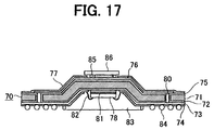
- Fig. 17 shows a BGA package according to a fifth preferred embodiment of the present invention.
- Figs. 18 and 19 show a substrate (70) used for fabricating the BGA package, shown in Fig. 17.
- the BGA package includes a substrate 70, which includes a copper plate 71.
- the copper plate 41 is provided on a front surface with an insulating layer 72 of polyimide having a thickness of 10 to 30 ⁇ m.
- a copper wiring pattern 73 is formed on the insulating layer 72.
- a solder resist 74 is formed (spread) over the copper wiring pattern 73 except some areas thereon.
- the copper plate 71 is provided on a rear surface with another insulating layer 75 of polyimide having a thickness of 10 to 30 ⁇ m, as shown in Fig. 19.
- Another copper wiring pattern 76 is formed on the insulating layer 75 to have a thickness of 12 to 35 ⁇ m.
- Another solder resist 77 is formed (spread) over the copper wiring pattern 76 except some areas thereon.
- the substrate 70 includes the copper plate 71, insulating layers 72 and 75, and copper wiring patterns 73 and 76.
- a metal mold reduction (drawing) process is carried out to the substrate 70 to form a cavity 79 at the front surface in which a semiconductor chip 78 is placed.
- the copper plate 71 is provided therein with through holes 80, which connect the front surface and rear surface thereof.
- One ends of the copper wiring pattern 73 form bonding posts 73a, which are to be connected to bonding wires 82.
- One ends of the copper wiring pattern 76 form lands 76a, which are to be connected to solder balls 85.
- the lands 76a are coated with thermally stable OSP (Organic Solder Preservative).
- the other ends of the copper wiring pattern 76 are connected to the through holes 80.
- an insulating paste 81 is formed (spread) over so that the semiconductor chip 78 is well fixed at the rear surface in the cavity 79.
- the semiconductor chip 78 is provided at the rear surface with no electrodes.
- the semiconductor chip 78 is connected at the electrodes to the copper wiring pattern 73 by the bonding wires 82.
- the cavity 79 is to be filled up with an epoxy resin 83.
- the substrate 70 is provided at the front surface with solder balls 84, which are arranged in lattice manner.
- the solder balls 84 are arranged at exposed regions of the solder resist 77.
- Each of the through holes 80 is connected to the solder balls 84.
- the BGA package further includes a semiconductor device 86, which is mounted on the rear surface of the substrate 70.
- the semiconductor device 86 may be of a chip-size-package type, in which only solder balls 85 are exposed from an electrode surface thereof.
- the semiconductor device 86 is connected at terminals via the solder balls 85 to the lands 76a of the copper wiring pattern 76.
- solder balls 85 of the semiconductor device 86 are connected to the lands 76a.
- solder balls 84 are formed on the front surface of the substrate 70, so that the solder balls 84 can be prevented from being changed in shape.
- the excess terminals which are the solder balls 84 not connected to the semiconductor chip 78, can be used as terminals to be connected to the other semiconductor device 86.
- the semiconductor chips 78 and 86 are mounted on the both surface of the substrate 70, so that only a small area is needed to mount two semiconductor chips on the motherboard. It means that the motherboard can be designed smaller in size.
- the semiconductor device 86 is a package type, which has been sealed when mounted on the substrate 70, so that no resin (57) is used. Therefore, the BGA packaged can be fabricated with a lower cost.
- the present invention is not limited by the above described embodiments, but a variety of modifications or changes may be applied.
- the semiconductor chips 28 and 48 are first mounted on the substrates 20 and 40, the other semiconductor chips 36 and 56 can be mounted first.
Landscapes
- Wire Bonding (AREA)
Applications Claiming Priority (2)
| Application Number | Priority Date | Filing Date | Title |
|---|---|---|---|
| JP30249799A JP3485507B2 (ja) | 1999-10-25 | 1999-10-25 | 半導体装置 |
| JP30249799 | 1999-10-25 |
Publications (2)
| Publication Number | Publication Date |
|---|---|
| EP1096567A2 true EP1096567A2 (de) | 2001-05-02 |
| EP1096567A3 EP1096567A3 (de) | 2003-09-10 |
Family
ID=17909680
Family Applications (1)
| Application Number | Title | Priority Date | Filing Date |
|---|---|---|---|
| EP00106301A Withdrawn EP1096567A3 (de) | 1999-10-25 | 2000-03-22 | KMG und seine Herstellung |
Country Status (3)
| Country | Link |
|---|---|
| US (1) | US6472732B1 (de) |
| EP (1) | EP1096567A3 (de) |
| JP (1) | JP3485507B2 (de) |
Cited By (1)
| Publication number | Priority date | Publication date | Assignee | Title |
|---|---|---|---|---|
| EP1432033A1 (de) * | 2002-12-17 | 2004-06-23 | Delphi Technologies, Inc. | Multichip-modul und Herstellungsverfahren |
Families Citing this family (45)
| Publication number | Priority date | Publication date | Assignee | Title |
|---|---|---|---|---|
| US6916682B2 (en) * | 2001-11-08 | 2005-07-12 | Freescale Semiconductor, Inc. | Semiconductor package device for use with multiple integrated circuits in a stacked configuration and method of formation and testing |
| US6617181B1 (en) * | 2002-02-01 | 2003-09-09 | Lsi Logic Corporation | Flip chip testing |
| US7064426B2 (en) | 2002-09-17 | 2006-06-20 | Chippac, Inc. | Semiconductor multi-package module having wire bond interconnect between stacked packages |
| US20040061213A1 (en) * | 2002-09-17 | 2004-04-01 | Chippac, Inc. | Semiconductor multi-package module having package stacked over die-up flip chip ball grid array package and having wire bond interconnect between stacked packages |
| US7053476B2 (en) * | 2002-09-17 | 2006-05-30 | Chippac, Inc. | Semiconductor multi-package module having package stacked over die-down flip chip ball grid array package and having wire bond interconnect between stacked packages |
| US7205647B2 (en) * | 2002-09-17 | 2007-04-17 | Chippac, Inc. | Semiconductor multi-package module having package stacked over ball grid array package and having wire bond interconnect between stacked packages |
| US6972481B2 (en) * | 2002-09-17 | 2005-12-06 | Chippac, Inc. | Semiconductor multi-package module including stacked-die package and having wire bond interconnect between stacked packages |
| US6838761B2 (en) * | 2002-09-17 | 2005-01-04 | Chippac, Inc. | Semiconductor multi-package module having wire bond interconnect between stacked packages and having electrical shield |
| US7034387B2 (en) * | 2003-04-04 | 2006-04-25 | Chippac, Inc. | Semiconductor multipackage module including processor and memory package assemblies |
| US6933598B2 (en) | 2002-10-08 | 2005-08-23 | Chippac, Inc. | Semiconductor stacked multi-package module having inverted second package and electrically shielded first package |
| JP2004200464A (ja) * | 2002-12-19 | 2004-07-15 | Anden | 金属配線板 |
| US6879028B2 (en) * | 2003-02-21 | 2005-04-12 | Freescale Semiconductor, Inc. | Multi-die semiconductor package |
| US20040217471A1 (en) * | 2003-02-27 | 2004-11-04 | Tessera, Inc. | Component and assemblies with ends offset downwardly |
| US7239024B2 (en) * | 2003-04-04 | 2007-07-03 | Thomas Joel Massingill | Semiconductor package with recess for die |
| KR101076537B1 (ko) * | 2003-12-17 | 2011-10-24 | 스태츠 칩팩, 엘티디. | 다이 위에 적층된 역전된 패키지를 구비한 멀티 칩 패키지모듈 |
| JP2005317861A (ja) | 2004-04-30 | 2005-11-10 | Toshiba Corp | 半導体装置およびその製造方法 |
| US8552551B2 (en) * | 2004-05-24 | 2013-10-08 | Chippac, Inc. | Adhesive/spacer island structure for stacking over wire bonded die |
| US20050258527A1 (en) * | 2004-05-24 | 2005-11-24 | Chippac, Inc. | Adhesive/spacer island structure for multiple die package |
| US20050269692A1 (en) | 2004-05-24 | 2005-12-08 | Chippac, Inc | Stacked semiconductor package having adhesive/spacer structure and insulation |
| US7253511B2 (en) * | 2004-07-13 | 2007-08-07 | Chippac, Inc. | Semiconductor multipackage module including die and inverted land grid array package stacked over ball grid array package |
| US7405474B1 (en) * | 2004-10-12 | 2008-07-29 | Cypress Semiconductor Corporation | Low cost thermally enhanced semiconductor package |
| US20080203552A1 (en) * | 2005-02-15 | 2008-08-28 | Unisemicon Co., Ltd. | Stacked Package and Method of Fabricating the Same |
| JP2008535273A (ja) * | 2005-03-31 | 2008-08-28 | スタッツ・チップパック・リミテッド | 上面および下面に露出した基板表面を有する半導体積層型パッケージアセンブリ |
| US7429787B2 (en) * | 2005-03-31 | 2008-09-30 | Stats Chippac Ltd. | Semiconductor assembly including chip scale package and second substrate with exposed surfaces on upper and lower sides |
| US7364945B2 (en) | 2005-03-31 | 2008-04-29 | Stats Chippac Ltd. | Method of mounting an integrated circuit package in an encapsulant cavity |
| US7429786B2 (en) * | 2005-04-29 | 2008-09-30 | Stats Chippac Ltd. | Semiconductor package including second substrate and having exposed substrate surfaces on upper and lower sides |
| US7354800B2 (en) | 2005-04-29 | 2008-04-08 | Stats Chippac Ltd. | Method of fabricating a stacked integrated circuit package system |
| US7582960B2 (en) | 2005-05-05 | 2009-09-01 | Stats Chippac Ltd. | Multiple chip package module including die stacked over encapsulated package |
| US7394148B2 (en) * | 2005-06-20 | 2008-07-01 | Stats Chippac Ltd. | Module having stacked chip scale semiconductor packages |
| TWI261350B (en) * | 2005-09-02 | 2006-09-01 | Wintek Corp | Electronic member with conductive connection structure |
| US7511371B2 (en) * | 2005-11-01 | 2009-03-31 | Sandisk Corporation | Multiple die integrated circuit package |
| US7352058B2 (en) * | 2005-11-01 | 2008-04-01 | Sandisk Corporation | Methods for a multiple die integrated circuit package |
| US7511359B2 (en) * | 2005-12-29 | 2009-03-31 | Intel Corporation | Dual die package with high-speed interconnect |
| US7768125B2 (en) | 2006-01-04 | 2010-08-03 | Stats Chippac Ltd. | Multi-chip package system |
| US7456088B2 (en) | 2006-01-04 | 2008-11-25 | Stats Chippac Ltd. | Integrated circuit package system including stacked die |
| US7750482B2 (en) | 2006-02-09 | 2010-07-06 | Stats Chippac Ltd. | Integrated circuit package system including zero fillet resin |
| US8704349B2 (en) | 2006-02-14 | 2014-04-22 | Stats Chippac Ltd. | Integrated circuit package system with exposed interconnects |
| JP2007305955A (ja) * | 2006-04-10 | 2007-11-22 | Toshiba Corp | 半導体装置及びその製造方法 |
| KR20090012933A (ko) * | 2007-07-31 | 2009-02-04 | 삼성전자주식회사 | 반도체 패키지, 스택 모듈, 카드, 시스템 및 반도체패키지의 제조 방법 |
| JP5110441B2 (ja) * | 2008-01-15 | 2012-12-26 | 大日本印刷株式会社 | 半導体装置用配線部材、半導体装置用複合配線部材、および樹脂封止型半導体装置 |
| US8159830B2 (en) * | 2009-04-17 | 2012-04-17 | Atmel Corporation | Surface mounting chip carrier module |
| KR102059402B1 (ko) * | 2013-04-15 | 2019-12-26 | 삼성전자주식회사 | 전자소자 패키지 및 이에 사용되는 패키지 기판 |
| DE102013219992A1 (de) * | 2013-10-02 | 2015-04-02 | Conti Temic Microelectronic Gmbh | Schaltungsvorrichtung und Verfahren zu deren Herstellung |
| KR102243285B1 (ko) * | 2014-07-01 | 2021-04-23 | 삼성전자주식회사 | 반도체 패키지 |
| CN107564877A (zh) * | 2016-06-30 | 2018-01-09 | 华邦电子股份有限公司 | 半导体元件封装体及半导体元件封装制程 |
Citations (3)
| Publication number | Priority date | Publication date | Assignee | Title |
|---|---|---|---|---|
| US5280192A (en) * | 1990-04-30 | 1994-01-18 | International Business Machines Corporation | Three-dimensional memory card structure with internal direct chip attachment |
| WO1997036325A1 (en) * | 1996-03-25 | 1997-10-02 | Micromodule Systems | Packaging and interconnect system for integrated circuits |
| US5936305A (en) * | 1997-11-20 | 1999-08-10 | Micron Technology, Inc. | Stacked leads-over chip multi-chip module |
Family Cites Families (21)
| Publication number | Priority date | Publication date | Assignee | Title |
|---|---|---|---|---|
| US4987100A (en) * | 1988-05-26 | 1991-01-22 | International Business Machines Corporation | Flexible carrier for an electronic device |
| US5200362A (en) * | 1989-09-06 | 1993-04-06 | Motorola, Inc. | Method of attaching conductive traces to an encapsulated semiconductor die using a removable transfer film |
| DE3935680A1 (de) * | 1989-10-26 | 1991-05-02 | Standard Elektrik Lorenz Ag | Verfahren zum herstellen einer metallkern-leiterplatte |
| JP2701589B2 (ja) * | 1991-06-26 | 1998-01-21 | 日本電気株式会社 | 半導体装置及びその製造方法 |
| JP2819523B2 (ja) * | 1992-10-09 | 1998-10-30 | インターナショナル・ビジネス・マシーンズ・コーポレイション | 印刷配線板及びその製造方法 |
| JPH08167630A (ja) * | 1994-12-15 | 1996-06-25 | Hitachi Ltd | チップ接続構造 |
| US5798564A (en) * | 1995-12-21 | 1998-08-25 | Texas Instruments Incorporated | Multiple chip module apparatus having dual sided substrate |
| JP2828053B2 (ja) * | 1996-08-15 | 1998-11-25 | 日本電気株式会社 | 半導体装置 |
| JPH1079405A (ja) * | 1996-09-04 | 1998-03-24 | Hitachi Ltd | 半導体装置およびそれが実装された電子部品 |
| JPH1093013A (ja) * | 1996-09-17 | 1998-04-10 | Seiko Epson Corp | 半導体装置 |
| JPH10270497A (ja) * | 1997-03-27 | 1998-10-09 | Sumitomo Bakelite Co Ltd | 半導体素子固定方法 |
| JPH10270477A (ja) * | 1997-03-27 | 1998-10-09 | Hitachi Ltd | 半導体パッケージ製造方法 |
| US5869889A (en) * | 1997-04-21 | 1999-02-09 | Lsi Logic Corporation | Thin power tape ball grid array package |
| US5900675A (en) * | 1997-04-21 | 1999-05-04 | International Business Machines Corporation | Organic controlled collapse chip connector (C4) ball grid array (BGA) chip carrier with dual thermal expansion rates |
| US5981312A (en) * | 1997-06-27 | 1999-11-09 | International Business Machines Corporation | Method for injection molded flip chip encapsulation |
| JPH1174421A (ja) * | 1997-08-30 | 1999-03-16 | Mitsui High Tec Inc | 複合型半導体装置 |
| DE69934153T2 (de) * | 1998-02-02 | 2007-09-20 | Shin-Etsu Chemical Co., Ltd. | Verfahren zur Montage von Flip-Chip-Halbleiterbauelementen |
| JPH11233571A (ja) * | 1998-02-12 | 1999-08-27 | Hitachi Ltd | 半導体装置及びアンダーフィル材並びに熱硬化性フィルム材 |
| JPH11251360A (ja) * | 1998-03-04 | 1999-09-17 | Toshiba Corp | 半導体装置およびその製造方法 |
| JP3648053B2 (ja) * | 1998-04-30 | 2005-05-18 | 沖電気工業株式会社 | 半導体装置 |
| US6232667B1 (en) * | 1999-06-29 | 2001-05-15 | International Business Machines Corporation | Technique for underfilling stacked chips on a cavity MLC module |
-
1999
- 1999-10-25 JP JP30249799A patent/JP3485507B2/ja not_active Expired - Fee Related
-
2000
- 2000-03-21 US US09/532,028 patent/US6472732B1/en not_active Expired - Fee Related
- 2000-03-22 EP EP00106301A patent/EP1096567A3/de not_active Withdrawn
Patent Citations (3)
| Publication number | Priority date | Publication date | Assignee | Title |
|---|---|---|---|---|
| US5280192A (en) * | 1990-04-30 | 1994-01-18 | International Business Machines Corporation | Three-dimensional memory card structure with internal direct chip attachment |
| WO1997036325A1 (en) * | 1996-03-25 | 1997-10-02 | Micromodule Systems | Packaging and interconnect system for integrated circuits |
| US5936305A (en) * | 1997-11-20 | 1999-08-10 | Micron Technology, Inc. | Stacked leads-over chip multi-chip module |
Cited By (2)
| Publication number | Priority date | Publication date | Assignee | Title |
|---|---|---|---|---|
| EP1432033A1 (de) * | 2002-12-17 | 2004-06-23 | Delphi Technologies, Inc. | Multichip-modul und Herstellungsverfahren |
| US6833628B2 (en) | 2002-12-17 | 2004-12-21 | Delphi Technologies, Inc. | Mutli-chip module |
Also Published As
| Publication number | Publication date |
|---|---|
| EP1096567A3 (de) | 2003-09-10 |
| JP3485507B2 (ja) | 2004-01-13 |
| US6472732B1 (en) | 2002-10-29 |
| JP2001127186A (ja) | 2001-05-11 |
Similar Documents
| Publication | Publication Date | Title |
|---|---|---|
| US6472732B1 (en) | BGA package and method for fabricating the same | |
| KR100511728B1 (ko) | 복수의 반도체 칩을 고밀도로 실장할 수 있는 소형 반도체장치 및 그의 제조 방법 | |
| US5977633A (en) | Semiconductor device with metal base substrate having hollows | |
| US6528869B1 (en) | Semiconductor package with molded substrate and recessed input/output terminals | |
| US5977641A (en) | Semiconductor device and method for manufacturing the same | |
| US7173330B2 (en) | Multiple chip semiconductor package | |
| TWI426586B (zh) | 具有用於將焊墊鍍於晶片下方之導線的球柵陣列封裝 | |
| US7253503B1 (en) | Integrated circuit device packages and substrates for making the packages | |
| US6380048B1 (en) | Die paddle enhancement for exposed pad in semiconductor packaging | |
| KR100385766B1 (ko) | 외부 접속 전극들에 대응하여 분리 제공된 수지 부재들을구비하는 반도체 디바이스 | |
| KR100960739B1 (ko) | 열적으로 향상된 반도체 볼 그리드 어레이 디바이스 및 그제조 방법 | |
| US5838061A (en) | Semiconductor package including a semiconductor chip adhesively bonded thereto | |
| US7749806B2 (en) | Fabricating process of a chip package structure | |
| US5636104A (en) | Printed circuit board having solder ball mounting groove pads and a ball grid array package using such a board | |
| KR100212607B1 (ko) | 반도체 칩 팩키지 | |
| US20030164543A1 (en) | Interposer configured to reduce the profiles of semiconductor device assemblies and packages including the same and methods | |
| US20110317388A1 (en) | Electronic device having a wiring substrate | |
| JPH08111433A (ja) | 半導体装置及び半導体装置製造用テープ | |
| JP2011238964A (ja) | 半導体パッケージおよびこの製造方法 | |
| JP3450236B2 (ja) | 半導体装置及びその製造方法 | |
| US20020079594A1 (en) | Semiconductor device and method of manufacture thereof, circuit board, and electronic instrument | |
| US6492715B1 (en) | Integrated semiconductor package | |
| KR20030081549A (ko) | 반도체소자 패키지 제조방법 | |
| US20020192869A1 (en) | Semiconductor package and fabrication method of the same | |
| US6812125B1 (en) | Substrate for semiconductor packaging |
Legal Events
| Date | Code | Title | Description |
|---|---|---|---|
| PUAI | Public reference made under article 153(3) epc to a published international application that has entered the european phase |
Free format text: ORIGINAL CODE: 0009012 |
|
| AK | Designated contracting states |
Kind code of ref document: A2 Designated state(s): AT BE CH CY DE DK ES FI FR GB GR IE IT LI LU MC NL PT SE |
|
| AX | Request for extension of the european patent |
Free format text: AL;LT;LV;MK;RO;SI |
|
| PUAL | Search report despatched |
Free format text: ORIGINAL CODE: 0009013 |
|
| AK | Designated contracting states |
Kind code of ref document: A3 Designated state(s): AT BE CH CY DE DK ES FI FR GB GR IE IT LI LU MC NL PT SE |
|
| AX | Request for extension of the european patent |
Extension state: AL LT LV MK RO SI |
|
| RIC1 | Information provided on ipc code assigned before grant |
Ipc: 7H 05K 3/44 B Ipc: 7H 01L 23/498 B Ipc: 7H 01L 21/56 B Ipc: 7H 01L 23/13 B Ipc: 7H 01L 25/065 A |
|
| 17P | Request for examination filed |
Effective date: 20040218 |
|
| AKX | Designation fees paid |
Designated state(s): DE FR GB NL |
|
| 17Q | First examination report despatched |
Effective date: 20080909 |
|
| STAA | Information on the status of an ep patent application or granted ep patent |
Free format text: STATUS: THE APPLICATION IS DEEMED TO BE WITHDRAWN |
|
| 18D | Application deemed to be withdrawn |
Effective date: 20100819 |