EP1100114A2 - Système de chauffage par rayonnement avec zone contrôlée utilisant un réflecteur focalisé - Google Patents
Système de chauffage par rayonnement avec zone contrôlée utilisant un réflecteur focalisé Download PDFInfo
- Publication number
- EP1100114A2 EP1100114A2 EP00309762A EP00309762A EP1100114A2 EP 1100114 A2 EP1100114 A2 EP 1100114A2 EP 00309762 A EP00309762 A EP 00309762A EP 00309762 A EP00309762 A EP 00309762A EP 1100114 A2 EP1100114 A2 EP 1100114A2
- Authority
- EP
- European Patent Office
- Prior art keywords
- temperature
- controller
- substrate
- signal
- heating elements
- Prior art date
- Legal status (The legal status is an assumption and is not a legal conclusion. Google has not performed a legal analysis and makes no representation as to the accuracy of the status listed.)
- Withdrawn
Links
Images


Classifications
-
- F—MECHANICAL ENGINEERING; LIGHTING; HEATING; WEAPONS; BLASTING
- F24—HEATING; RANGES; VENTILATING
- F24D—DOMESTIC- OR SPACE-HEATING SYSTEMS, e.g. CENTRAL HEATING SYSTEMS; DOMESTIC HOT-WATER SUPPLY SYSTEMS; ELEMENTS OR COMPONENTS THEREFOR
- F24D9/00—Central heating systems employing combinations of heat transfer fluids covered by two or more of groups F24D1/00 - F24D7/00
-
- H—ELECTRICITY
- H10—SEMICONDUCTOR DEVICES; ELECTRIC SOLID-STATE DEVICES NOT OTHERWISE PROVIDED FOR
- H10P—GENERIC PROCESSES OR APPARATUS FOR THE MANUFACTURE OR TREATMENT OF DEVICES COVERED BY CLASS H10
- H10P72/00—Handling or holding of wafers, substrates or devices during manufacture or treatment thereof
- H10P72/06—Apparatus for monitoring, sorting, marking, testing or measuring
- H10P72/0602—Temperature monitoring
-
- H—ELECTRICITY
- H10—SEMICONDUCTOR DEVICES; ELECTRIC SOLID-STATE DEVICES NOT OTHERWISE PROVIDED FOR
- H10P—GENERIC PROCESSES OR APPARATUS FOR THE MANUFACTURE OR TREATMENT OF DEVICES COVERED BY CLASS H10
- H10P72/00—Handling or holding of wafers, substrates or devices during manufacture or treatment thereof
- H10P72/04—Apparatus for manufacture or treatment
- H10P72/0431—Apparatus for thermal treatment
- H10P72/0436—Apparatus for thermal treatment mainly by radiation
Definitions
- the present invention relates generally to the field of semiconductor processing systems such as photoresist ashers, and more specifically to a zone controlled radiant heating device utilizing a focused reflector, for use in such systems.
- photolithography techniques are used to form integrated circuit patterns on a substrate.
- the substrate is coated with a photoresist, portions of which are exposed to ultraviolet (UV) radiation through a mask to image a desired circuit pattern on the photoresist.
- UV radiation ultraviolet
- the portions of the photoresist left unexposed to the UV radiation are removed by a processing solution, leaving only the exposed portions on the substrate. These remaining exposed portions are baked during a photostabilization process to enable the photoresist to withstand subsequent processing.
- the photoresist is “ashed” or “burned” and the ashed or burned photoresist, along with the residue, is “stripped” or “cleaned” from the surface of the substrate.
- One manner of removing photoresist and residues is by directing a microwave-energized plasma at the substrate surface.
- the substrate In a photoresist ashing process, the substrate is rapidly heated to a preset temperature by infrared radiation.
- exothermic reactions on the substrate surface, variations in direction of heat flow, and changing thermal radiation characteristics of the substrate can result in continuous thermal transients and temperature gradients on the substrate surface.
- Temperature gradients are often most pronounced during the ramping phase wherein the substrate temperature is raised to the desired level, although lesser gradients may remain when the substrate is maintained in the steady state phase at this desired level.
- Such thermal transients and temperature gradients are undesirable in an ashing process as non-uniform heating of the substrate typically results in non-uniform ashing of the photoresist.
- One approach to uniformly heating a substrate is to use a heating configuration utilizing a plurality of heating zones, the output radiation of each of which is directed to a specific zone of the substrate by a reflector.
- the shape of the reflector is not critically important because the heating zones are individually controlled, using separate feedback (e.g ., an optical pyrometer output signal) from each zone to aid in determining the zone power control signal.
- separate feedback e.g ., an optical pyrometer output signal
- such a system typically experiences a slower ramp rate than what can be maximally achieved with full power applied to each zone.
- such a system is not effective in low temperature processes because optical pyrometers typically do not work well under 200° C.
- a temperature control system for a plasma processing device.
- the plasma processing device comprises a plasma generator and a processing chamber in communication with the plasma generator such that plasma within the generator may pass into the chamber and react with the surface of a substrate residing therein.
- the temperature control system comprises (i) a radiant heater assembly for heating the substrate, comprising a plurality of radiant heating elements arranged in a plurality of zones, each zone comprising at least one heating element, and a focused reflector for focusing radiant energy from the heating elements toward the substrate; (ii) a feedback mechanism for providing a substrate temperature feedback signal; and (iii) a controller, including a P-I-D closed loop controller and a lamp power controller.
- the P-I-D controller receives an operator-selected process recipe (e.g ., wafer temperature setpoint, chamber wall temperature, gas mixture and mass flow rate), as well as the temperature feedback signal, and adjusts a control variable output to the power controller.
- the power controller operating parallel to but independent of the P-I-D controller, also receives the temperature feedback signal and compares it to the temperature setpoint signal. The power controller then adjusts the power applied to the plurality of zones of radiant heating elements.
- the power controller operates in at least a first ramp state and a second steady state, depending upon the magnitude of difference ( ⁇ ) between the temperature setpoint signal and the temperature feedback signal.
- the power controller can, independently of the control variable, adjust the power applied to the plurality of zones of radiant heating elements, in response to stored temperature zone maps.
- Zone maps can be stored in a processor memory in the form of look-up tables for a variety of system operating conditions for both the (i) ramp to setpoint temperature and (ii) steady state conditions.
- Zone maps allow the processor to control the output of the power controller, independently of the control variable signal from the P-I-D closed loop controller, by independent phase modulation of each zone in the lamp array.
- Zone maps for different process recipes allow for adjustment of the irradiance of different portions of the wafer, for example center to edge.
- the maps also allow the heating system to compensate for chamber geometry and wall temperature radiation cooling effects, in particular those which would cause severe temperature gradients from the center to the edge of the wafer during processing.
- the variable d is also stored in the form of a look-up table in the power controller processor memory.
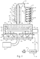
- Figure 1 discloses a photoresist asher 10 comprising a gas box 12; a microwave power generator assembly 14; a process chamber 16 in which is heated a semiconductor substrate such as a wafer 18; a radiant heater assembly 20 for heating the wafer 18, situated at the bottom of the process chamber; and a controller 22 for controlling the power to the radiant heater assembly.
- a temperature probe 24, such as a thermocouple, is used to monitor the temperature of the wafer 18 and provide a signal indicative thereof to the controller 22.
- a vacuum pump 26 is used to evacuate the process chamber 16 for processes requiring vacuum conditions.
- a monochromator 28 is used to monitor the optical emission characteristics of gases within the chamber to aid in process endpoint determination.
- a desired mixture of gases is introduced into a sapphire tube 32 from gas box 12 through an inlet conduit 34.
- the gases forming the desired mixture are stored in separate supplies (not shown) and mixed in the gas box 12 by means of valves 36 and piping 38.
- One example of a desired gas mixture is forming gas (primarily nitrogen with a small percentage of hydrogen), oxygen and carbon tetrafluoride.
- the desired gas mixture is energized by the microwave power generator assembly 14 to form a reactive plasma that will ash photoresist on the wafer 18 in the process chamber 16 when heated by the radiant heater assembly 20.
- a magnetron 40 generates microwave energy that is coupled to a waveguide 42. Microwave energy is fed from the waveguide through apertures (not shown) in microwave enclosure 44, which surrounds the sapphire tube 32.
- An outer quartz tube 46 surrounds the sapphire plasma tube 32, slightly separated therefrom. Pressurized air is fed into the gap between the tubes 32 and 46 to effectively cool the sapphire tube 32 during operation.
- the microwave enclosure is segmented into four sections 44a, 44b, 44c and 44d. Segmentation of the enclosure 44 prevents an unacceptably large thermal gradient from developing along its axial length when suitable input power is provided. Each segment of the enclosure is separately fed with microwave energy that passes through the quartz tube 46 and the sapphire tube 32 passing therethrough. Gas within the inner sapphire tube 32 is thereby energized to create a plasma. Microwave traps 48 and 50 are provided at the ends of the microwave enclosure 44 to prevent microwave leakage.
- the energized plasma enters the process chamber 16 through an opening (not shown) in the top wall 52 thereof.
- the reactive plasma ashes the photoresist on the wafer 18.
- the reactive plasma must be uniformly distributed across the surface of the wafer,
- the temperature of the reactive plasma must be maintained so as to minimize the heat energy applied to the wafer by the plasma, and (iii) a uniform temperature must be maintained across the surface of the wafer.
- An apertured, dual layered baffle plate assembly 54 comprised of upper baffle plate 54a and lower baffle plate 54b, evenly distributes the reactive plasma across the surface of the wafer 18 being processed, and reduces the temperature of the reactive plasma passing through the baffle plate assembly.
- the present invention is embodied in the combination of the radiant heater assembly 20 for heating the wafer 18, the controller 22 for controlling the power to the radiant heater assembly (including a P-I-D controller and a lamp controller), and the thermocouple 24 for providing wafer temperature feedback to the PID controller.
- the thermocouple provides accurate temperature feedback measurements under 200° C. This combination functions to maintain a uniform temperature across the surface of the wafer 18, within 2° C of the process setpoint temperature. Such temperature uniformity insures consistently uniform photoresist ashing rates.
- FIG 2 shows the radiant heater assembly 20 in plan view.
- the radiant heater assembly 20 comprises a reflector 56 and a plurality of tungsten halogen lamps 58 forming an inner annular array 60 and an outer annular array 62.
- the arrays may also be referred to as bulb rings or troughs.
- the lamps 58 in the inner annular array 60 are positioned circumferentially equidistant from each other within the trough of an inner annular reflector 64 having a generally semicircular or parabolic cross section.
- the lamps 58 in the outer annular array 62 are positioned circumferentially equidistant from each other within the trough of an outer annular reflector 66 having a semicircular or parabolic cross section (see Figure 1).
- the parabolic or semicircular (concave) reflector shape reflects and redirects the heat generated by the lamps toward the backside of the wafer 18 positioned within the process chamber 16 on pins 68 (see Figure 1).
- the outer edge of the outer annular reflector 66 extends at least as far radially outward as the outer edge of the wafer positioned thereabove to prevent edge cooling effects.
- No lamp 58 is positioned at a central opening 70 of the reflector 56 because the center of the wafer typically experiences the highest temperature during heating.
- the central opening 70 in the reflector also provides a path through which the process chamber 16 may be evacuated by vacuum pump 26 (see Figure 1).
- inner annular lamp array 60 and the outer annular lamp array 62 are segmented into zones (a-n) for control purposes.
- inner array 60 comprises eight lamps segmented into four zones, each comprising two adjacently positioned lamps.
- Outer array 62 comprises sixteen lamps segmented into eight zones, each comprising two adjacently positioned lamps.
- twenty-four total lamps 58 are divided into twelve zones (a-n) each comprising to adjacently positioned lamps.
- the number of zones (a-n) may be lesser or greater than twelve.
- adjacent zones are shown as being segmented by phantom radially extending lines.
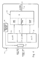
- FIG 3 is a more detailed block diagrammatic view of the controller 22 for the radiant heater assembly 20 shown in Figure 2.
- the controller 22 comprises first level control logic 74, second level control logic 76, and output power supplies 78a-78n, each of which drives one of the twelve zones of lamps 58.
- the first level control logic 74 is implemented in the disclosed embodiment as a closed loop P-I-D controller 80 that uses as inputs a wafer temperature feedback signal 25 from thermocouple 24, and a temperature setpoint signal 27 ( e.g. , 80° - 300° C) selected by an operator via a designated process recipe.
- the P-I-D controller 80 may include a comparator for comparing the signals 25 and 27, and an amplifier for amplifying the error signal represented by the difference between these two signals.
- the P-I-D controller 80 compares the wafer temperature feedback and the desired temperature setpoint. Based on the difference between these two signals, the P-I-D controller 80 outputs a variable control signal 89 to phase-modulated lamp power controller 90 within second level control logic 76. In response to the variable control signal 89, the lamp power controller 90 controls via control signals 92 the power supplied to the twelve zones of lamps 58 by output power supplies 78a-78n.
- a processor 87 within second level control logic 76 also receives as inputs the wafer temperature feedback signal 25 from thermocouple 24 and the temperature setpoint signal 27. Based on the difference in magnitude of these two signals, the processor determines whether the lamp power controller 90 should be operated in the ramp state 82 (initially), the steady state 84, or a transition state 86 (intermediate the ramp state and the steady state).
- the processor uses a look-up table or temperature zone map 88 within its operating software to determine what adjustments the lamp power controller 90 must make to power supplies 78a-78n to accommodate the temperatures required by a particular zone map for a particular state of operation.
- the processor 87 will re-set the per-zone power level for each of the twelve zones in the lamp arrays. This action by the processor 87 is independent of the variable control signal 89 received by the lamp power controller 90 from P-I-D controller 80.
- Temperature setpoint signals, such as setpoint signal 27, and the temperature zone maps 88 are stored in one or more memory devices (not shown).
- FIG 4 shows a more detailed block diagram of second level control logic 76 of the controller 22 of Figure 3.
- the processor 87 receives as inputs the desired temperature setpoint and the output of the thermocouple 24, which may be in the form of an analog voltage signal representative of their respective measurements. Based on the magnitude of the difference (delta ( ⁇ )) between the desired temperature setpoint 27 and the wafer temperature feedback 25, the processor determines in which state the radiant heater assembly 20 should be operated.
- the processor 87 initially issues a ramp state 82 signal to the lamp power controller 90 wherein each of the individual zone power supplies 78 are instructed to provide maximum power their respective zones.
- maximum power may not necessarily be full 100% power, but some lesser number such as 80% power, which will still achieve an acceptable and desired ramp rate. In the present invention, it has been found that 80% power to each of the zones will achieve an acceptable wafer temperature ramp rate of about 22-25° C per second. Individual zone control is not required upon initial ramping of the system in ramp state 82, because the reflector design supplies the required uniform irradiance. Thus, in the ramp state 82, the processor 87 provides a control signal to the lamp power controller 90 based only on the ramp state of operation as determined by the processor, and not the zone map 88 (being uniformly set to 80%).
- the processor 87 issues a transition state 86 signal to the lamp power controller 90.
- the processor 87 also looks to the temperature zone map 88 to determine the nature of the control signal to issue to the lamp power controller 90.
- the lamp power controller adjusts the signals 92 provided to the power supplies 78a-n based on this control signal (and the variable control signal 89 output by the P-I-D controller 80).
- the temperature zone map 88 is essentially a look-up table that stores input power requirements for the different wafer zones in lamp arrays 60 and 62, based on empirical process data obtained for different process temperatures and wafer types and sizes.
- the temperature zone map may also be modified to compensate for geometries in the process chamber 52 design or known heat loss areas within the chamber that may affect wafer heating.
- the temperature zone map 88 can identify and distinguish between a first set of zone input power requirements for a 270° C wafer process temperature carried out in a process chamber 52 having walls maintained at 15° C, and a second set of zone input power requirements for a 100° C wafer process temperature carried out in a process chamber 52 having walls maintained at 30° C.
- Any number of process recipes may be stored (mapped) and indirectly accessed by an operator. Based on a process recipe that the operator chooses, operating software selects the particular zone map 88 to be provided to the processor 87.
- the processor 87 will provide a control signal to the lamp power controller 90.
- the control signal will reduce the power supplied to the lamp array so that the rate of wafer heat increase is slowed, as compared to the time-averaged ramp rate, as the wafer temperature approaches its desired setpoint.
- the processor 87 issues a steady state 86 signal to the lamp power controller 90. Again, the processor 87 will provide a control signal to the lamp power controller 90 based on the steady state status and the selected temperature zone map 88. Typically (but not always), for a given selected zone map, the control signal in the steady state will instruct the power controller 90 to further reduce the power levels applied to the inner and outer lamp arrays via control signals 92.
- the power levels for the inner and outer arrays are likely to differ in the steady state.
- zones in the outer array 62 may be operated at 70% power, while the zones in the inner array 60 may be operated at 50% power to control for heat losses at the wafer edges that are inherent in a cold wall processing system.
- not all of the zones in an array must be operated at the same power level. Variations in power levels for different zones within the same array may be necessary to compensate for other factors such as chamber geometries or known areas of heat loss within the chamber, including the process chamber wafer loading slot and door assembly.
- wafer temperature feedback is used by the P-I-D controller 80 to adjust the lamp power controller 90 to maintain the wafer temperature at the point of measurement to within 2% of the process temperature setpoint.
- the lamp power controller 90 also regulates power internally per the appropriate zone map 88, in this case the steady state.
- the actual applied power per the above example, would be 70% of what the P-I-D controller output signal 89 requested (for the outer array zones) and 50% of what the P-I-D controller output signal 89 requested (for the inner array zones).
- One or more temperature sensors 72 are mounted on the interior of process chamber wall 52 to provide an indication of wall temperature. Such sensors are used in the heating/cooling system for maintaining process wall temperature, but are not used as direct inputs to the zone controlled radiant wafer heating system of the present invention. However, because the temperature zone maps directly influence the wafer heating system of the present invention, and are based in part on process chamber wall temperatures, the temperature sensors and chamber wall heating/cooling systems must work effectively to provide an accurate and reliable wafer heating system.
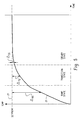
- Figure 5 is a graphical representation of wafer temperature versus time.
- the temperature of the wafer, as provided by feedback thermocouple 24, is shown in the ramp, transition, and steady states of operation.
- the difference (delta ( ⁇ )) between the desired temperature setpoint 27 and the wafer temperature feedback 25, is shown for each state ( ⁇ RS , ⁇ TS , and ⁇ SS , respectively).
- the present invention provides for a close approximation of temperature to the desired setpoint without any overshoot. If a minimal amount of temperature overshoot is acceptable, the intermediate transition phase of operation may be eliminated in favor of a two phase (ramp and steady state) operation, such that the temperature setpoint may be more quickly achieved.
Landscapes
- Engineering & Computer Science (AREA)
- Physics & Mathematics (AREA)
- Thermal Sciences (AREA)
- Chemical & Material Sciences (AREA)
- Combustion & Propulsion (AREA)
- Mechanical Engineering (AREA)
- General Engineering & Computer Science (AREA)
- Drying Of Semiconductors (AREA)
- Exposure Of Semiconductors, Excluding Electron Or Ion Beam Exposure (AREA)
- Plasma Technology (AREA)
- Photosensitive Polymer And Photoresist Processing (AREA)
- Chemical Vapour Deposition (AREA)
Applications Claiming Priority (2)
| Application Number | Priority Date | Filing Date | Title |
|---|---|---|---|
| US436681 | 1999-11-09 | ||
| US09/436,681 US6259072B1 (en) | 1999-11-09 | 1999-11-09 | Zone controlled radiant heating system utilizing focused reflector |
Publications (2)
| Publication Number | Publication Date |
|---|---|
| EP1100114A2 true EP1100114A2 (fr) | 2001-05-16 |
| EP1100114A3 EP1100114A3 (fr) | 2003-06-18 |
Family
ID=23733396
Family Applications (1)
| Application Number | Title | Priority Date | Filing Date |
|---|---|---|---|
| EP00309762A Withdrawn EP1100114A3 (fr) | 1999-11-09 | 2000-11-03 | Système de chauffage par rayonnement avec zone contrôlée utilisant un réflecteur focalisé |
Country Status (5)
| Country | Link |
|---|---|
| US (1) | US6259072B1 (fr) |
| EP (1) | EP1100114A3 (fr) |
| JP (1) | JP4868193B2 (fr) |
| KR (1) | KR100674764B1 (fr) |
| TW (1) | TW472291B (fr) |
Cited By (4)
| Publication number | Priority date | Publication date | Assignee | Title |
|---|---|---|---|---|
| WO2003014645A3 (fr) * | 2001-08-08 | 2003-05-08 | Applied Materials Inc | Tete de lampe amelioree pour chambre de traitement thermique rapide |
| WO2004073050A1 (fr) * | 2003-02-10 | 2004-08-26 | Axcelis Technologies Inc. | Source de chauffage rayonnante |
| WO2011103391A3 (fr) * | 2010-02-19 | 2012-02-09 | Applied Materials, Inc. | Dispositif de commande d'élément chauffant de haute précision et à haut rendement |
| EP1995766A3 (fr) * | 2007-05-20 | 2012-09-19 | Applied Materials, Inc. | Méthode de recuit contrôlé |
Families Citing this family (40)
| Publication number | Priority date | Publication date | Assignee | Title |
|---|---|---|---|---|
| US6333493B1 (en) | 1999-09-21 | 2001-12-25 | Kabushiki Kaisha Toshiba | Heat treating method and heat treating apparatus |
| JP4698807B2 (ja) * | 2000-09-26 | 2011-06-08 | 東京エレクトロン株式会社 | 半導体基板熱処理装置 |
| US6492625B1 (en) * | 2000-09-27 | 2002-12-10 | Emcore Corporation | Apparatus and method for controlling temperature uniformity of substrates |
| US6761796B2 (en) * | 2001-04-06 | 2004-07-13 | Axcelis Technologies, Inc. | Method and apparatus for micro-jet enabled, low-energy ion generation transport in plasma processing |
| KR100426274B1 (ko) * | 2001-08-02 | 2004-04-08 | 피에스케이 주식회사 | 램프가열을 이용한 반도체 웨이퍼 애싱장치 및 방법 |
| KR20030065217A (ko) * | 2002-01-31 | 2003-08-06 | 삼성전자주식회사 | 웨이퍼 척 및 이를 포함하는 웨이퍼 가공 장치 |
| KR100481180B1 (ko) * | 2002-09-10 | 2005-04-07 | 삼성전자주식회사 | 포토레지스트 제거방법 |
| US20040265409A1 (en) * | 2003-05-21 | 2004-12-30 | Stephen Keeley | Closed loop oven control system and method |
| US8580076B2 (en) * | 2003-05-22 | 2013-11-12 | Lam Research Corporation | Plasma apparatus, gas distribution assembly for a plasma apparatus and processes therewith |
| US20040235299A1 (en) * | 2003-05-22 | 2004-11-25 | Axcelis Technologies, Inc. | Plasma ashing apparatus and endpoint detection process |
| US7892357B2 (en) * | 2004-01-12 | 2011-02-22 | Axcelis Technologies, Inc. | Gas distribution plate assembly for plasma reactors |
| US20050247266A1 (en) * | 2004-05-04 | 2005-11-10 | Patel Nital S | Simultaneous control of deposition time and temperature of multi-zone furnaces |
| US8615886B1 (en) * | 2004-05-06 | 2013-12-31 | Winthrop D. Childers | Shaving system with energy imparting device |
| US20050250346A1 (en) * | 2004-05-06 | 2005-11-10 | Applied Materials, Inc. | Process and apparatus for post deposition treatment of low k dielectric materials |
| US7521653B2 (en) * | 2004-08-03 | 2009-04-21 | Exatec Llc | Plasma arc coating system |
| JP2006073895A (ja) * | 2004-09-03 | 2006-03-16 | Canon Inc | 冷却装置、露光装置及びデバイス製造方法 |
| US20060251827A1 (en) * | 2005-05-09 | 2006-11-09 | Applied Materials, Inc. | Tandem uv chamber for curing dielectric materials |
| US20060249175A1 (en) * | 2005-05-09 | 2006-11-09 | Applied Materials, Inc. | High efficiency UV curing system |
| US20090071951A1 (en) * | 2006-02-28 | 2009-03-19 | Toyota Jidosha Kabushiki Kaisha | Temperature Control Apparatus for Heater-Equipped Sensor |
| US7655933B2 (en) * | 2006-08-15 | 2010-02-02 | Varian Semiconductor Equipment Associates, Inc. | Techniques for temperature-controlled ion implantation |
| US8450193B2 (en) * | 2006-08-15 | 2013-05-28 | Varian Semiconductor Equipment Associates, Inc. | Techniques for temperature-controlled ion implantation |
| CN101688306B (zh) * | 2007-05-17 | 2011-08-17 | 埃克阿泰克有限责任公司 | 用于在共用等离子涂覆区沉积多种涂覆材料的装置与方法 |
| US7848840B2 (en) * | 2008-01-04 | 2010-12-07 | Applied Materials, Inc. | Method of controlling process parameters for semiconductor manufacturing apparatus |
| US20090194024A1 (en) * | 2008-01-31 | 2009-08-06 | Applied Materials, Inc. | Cvd apparatus |
| JP5169299B2 (ja) * | 2008-02-22 | 2013-03-27 | 株式会社デンソー | 半導体製造装置 |
| JP5236591B2 (ja) * | 2009-08-04 | 2013-07-17 | 株式会社アルバック | プラズマ処理装置 |
| US10504719B2 (en) | 2012-04-25 | 2019-12-10 | Applied Materials, Inc. | Cooled reflective adapter plate for a deposition chamber |
| US10145013B2 (en) | 2014-01-27 | 2018-12-04 | Veeco Instruments Inc. | Wafer carrier having retention pockets with compound radii for chemical vapor desposition systems |
| US10067006B2 (en) | 2014-06-19 | 2018-09-04 | Elwha Llc | Nanostructure sensors and sensing systems |
| KR101605717B1 (ko) | 2014-07-16 | 2016-03-23 | 세메스 주식회사 | 기판 처리 장치 및 기판 처리 방법 |
| US9779974B2 (en) | 2015-06-22 | 2017-10-03 | Lam Research Corporation | System and method for reducing temperature transition in an electrostatic chuck |
| US10763142B2 (en) | 2015-06-22 | 2020-09-01 | Lam Research Corporation | System and method for determining field non-uniformities of a wafer processing chamber using a wafer processing parameter |
| US10386821B2 (en) | 2015-06-22 | 2019-08-20 | Lam Research Corporation | Systems and methods for calibrating scalar field contribution values for a limited number of sensors including a temperature value of an electrostatic chuck and estimating temperature distribution profiles based on calibrated values |
| US10381248B2 (en) * | 2015-06-22 | 2019-08-13 | Lam Research Corporation | Auto-correction of electrostatic chuck temperature non-uniformity |
| JP2018531324A (ja) * | 2015-10-09 | 2018-10-25 | 北京北方華創微電子装備有限公司Beijing Naura Microelectronics Equipment Co., Ltd. | 加熱装置および加熱チャンバ |
| US9826574B2 (en) * | 2015-10-28 | 2017-11-21 | Watlow Electric Manufacturing Company | Integrated heater and sensor system |
| JP6512089B2 (ja) | 2015-12-15 | 2019-05-15 | 東京エレクトロン株式会社 | 基板処理装置及び基板処理装置の調整方法 |
| US11430639B2 (en) * | 2018-12-13 | 2022-08-30 | Xia Tai Xin Semiconductor (Qing Dao) Ltd. | Plasma processing system |
| US12225635B2 (en) | 2020-08-12 | 2025-02-11 | Watlow Electric Manufacturing Company | Method and system for providing variable ramp-up control for an electric heater |
| CN115985754B (zh) * | 2022-12-01 | 2026-01-09 | 中国原子能科学研究院 | 离子源 |
Family Cites Families (21)
| Publication number | Priority date | Publication date | Assignee | Title |
|---|---|---|---|---|
| JPS61196515A (ja) * | 1985-02-26 | 1986-08-30 | Mitsubishi Electric Corp | 帯域溶融型半導体製造装置 |
| US4680451A (en) * | 1985-07-29 | 1987-07-14 | A. G. Associates | Apparatus using high intensity CW lamps for improved heat treating of semiconductor wafers |
| US4640224A (en) * | 1985-08-05 | 1987-02-03 | Spectrum Cvd, Inc. | CVD heat source |
| US4981815A (en) | 1988-05-09 | 1991-01-01 | Siemens Aktiengesellschaft | Method for rapidly thermally processing a semiconductor wafer by irradiation using semicircular or parabolic reflectors |
| US5155336A (en) * | 1990-01-19 | 1992-10-13 | Applied Materials, Inc. | Rapid thermal heating apparatus and method |
| US5179677A (en) | 1990-08-16 | 1993-01-12 | Applied Materials, Inc. | Apparatus and method for substrate heating utilizing various infrared means to achieve uniform intensity |
| US5446825A (en) | 1991-04-24 | 1995-08-29 | Texas Instruments Incorporated | High performance multi-zone illuminator module for semiconductor wafer processing |
| US5436172A (en) * | 1991-05-20 | 1995-07-25 | Texas Instruments Incorporated | Real-time multi-zone semiconductor wafer temperature and process uniformity control system |
| US5268989A (en) | 1992-04-16 | 1993-12-07 | Texas Instruments Incorporated | Multi zone illuminator with embeded process control sensors and light interference elimination circuit |
| JP3195678B2 (ja) * | 1993-01-22 | 2001-08-06 | 東京エレクトロン株式会社 | エネルギー線加熱装置 |
| JPH0637009A (ja) * | 1992-07-14 | 1994-02-10 | Fujitsu Ltd | アッシング装置 |
| US5418885A (en) * | 1992-12-29 | 1995-05-23 | North Carolina State University | Three-zone rapid thermal processing system utilizing wafer edge heating means |
| US5561612A (en) * | 1994-05-18 | 1996-10-01 | Micron Technology, Inc. | Control and 3-dimensional simulation model of temperature variations in a rapid thermal processing machine |
| JPH08167590A (ja) * | 1994-12-13 | 1996-06-25 | Dainippon Screen Mfg Co Ltd | プラズマアッシング方法 |
| US5551985A (en) * | 1995-08-18 | 1996-09-03 | Torrex Equipment Corporation | Method and apparatus for cold wall chemical vapor deposition |
| US5850071A (en) * | 1996-02-16 | 1998-12-15 | Kokusai Electric Co., Ltd. | Substrate heating equipment for use in a semiconductor fabricating apparatus |
| DE69620590T2 (de) * | 1996-05-21 | 2002-11-21 | Applied Materials, Inc. | Verfahren und Vorrichtung zum Regeln der Temperatur einer Reaktorwand |
| US5788799A (en) * | 1996-06-11 | 1998-08-04 | Applied Materials, Inc. | Apparatus and method for cleaning of semiconductor process chamber surfaces |
| US5937142A (en) * | 1996-07-11 | 1999-08-10 | Cvc Products, Inc. | Multi-zone illuminator for rapid thermal processing |
| EP0823492A3 (fr) * | 1996-08-07 | 1999-01-20 | Concept Systems Design Inc. | Système de chauffage par zones avec réglage à contre-réaction |
| US6122440A (en) * | 1999-01-27 | 2000-09-19 | Regents Of The University Of Minnesota | Optical heating device for rapid thermal processing (RTP) system |
-
1999
- 1999-11-09 US US09/436,681 patent/US6259072B1/en not_active Expired - Lifetime
-
2000
- 2000-11-03 EP EP00309762A patent/EP1100114A3/fr not_active Withdrawn
- 2000-11-07 JP JP2000339066A patent/JP4868193B2/ja not_active Expired - Lifetime
- 2000-11-09 TW TW089123724A patent/TW472291B/zh not_active IP Right Cessation
- 2000-11-09 KR KR1020000066442A patent/KR100674764B1/ko not_active Expired - Fee Related
Cited By (9)
| Publication number | Priority date | Publication date | Assignee | Title |
|---|---|---|---|---|
| WO2003014645A3 (fr) * | 2001-08-08 | 2003-05-08 | Applied Materials Inc | Tete de lampe amelioree pour chambre de traitement thermique rapide |
| WO2004073050A1 (fr) * | 2003-02-10 | 2004-08-26 | Axcelis Technologies Inc. | Source de chauffage rayonnante |
| EP1995766A3 (fr) * | 2007-05-20 | 2012-09-19 | Applied Materials, Inc. | Méthode de recuit contrôlé |
| WO2011103391A3 (fr) * | 2010-02-19 | 2012-02-09 | Applied Materials, Inc. | Dispositif de commande d'élément chauffant de haute précision et à haut rendement |
| CN102763201A (zh) * | 2010-02-19 | 2012-10-31 | 应用材料公司 | 高效率高准确度加热器驱动器 |
| US8548312B2 (en) | 2010-02-19 | 2013-10-01 | Applied Materials, Inc. | High efficiency high accuracy heater driver |
| CN104617013A (zh) * | 2010-02-19 | 2015-05-13 | 应用材料公司 | 高效率高准确度加热器驱动器 |
| CN102763201B (zh) * | 2010-02-19 | 2015-07-15 | 应用材料公司 | 高效率高准确度加热器驱动器 |
| US9612020B2 (en) | 2010-02-19 | 2017-04-04 | Applied Materials, Inc. | High efficiency high accuracy heater driver |
Also Published As
| Publication number | Publication date |
|---|---|
| TW472291B (en) | 2002-01-11 |
| KR100674764B1 (ko) | 2007-01-25 |
| JP2001203195A (ja) | 2001-07-27 |
| JP4868193B2 (ja) | 2012-02-01 |
| US6259072B1 (en) | 2001-07-10 |
| EP1100114A3 (fr) | 2003-06-18 |
| KR20010051571A (ko) | 2001-06-25 |
Similar Documents
| Publication | Publication Date | Title |
|---|---|---|
| US6259072B1 (en) | Zone controlled radiant heating system utilizing focused reflector | |
| US5790750A (en) | Profiled substrate heating utilizing a support temperature and a substrate temperature | |
| US6782843B2 (en) | Actively-cooled distribution plate for reducing reactive gas temperature in a plasma processing system | |
| US5436172A (en) | Real-time multi-zone semiconductor wafer temperature and process uniformity control system | |
| US6225745B1 (en) | Dual plasma source for plasma process chamber | |
| KR101258287B1 (ko) | 플라즈마 리액터용 가스 분배 플레이트 어셈블리 | |
| US5446825A (en) | High performance multi-zone illuminator module for semiconductor wafer processing | |
| KR100784580B1 (ko) | 기판의 국부 가열 및 냉각 | |
| KR100587629B1 (ko) | 기판 표면에 걸쳐서 층류의 가스 흐름을 제공하는 가스분배판 조립체 | |
| CN109564845B (zh) | 用于等离子体室的隔离栅网 | |
| EP0916154B1 (fr) | Systeme d'echappement a double fenetre pour dispositif de traitement au plasma de tranches | |
| US20040026386A1 (en) | Method for improving ash rate uniformity in photoresist ashing process equipment | |
| CN113921451A (zh) | 载置台、处理基片的装置和对基片进行温度调节的方法 | |
| EP0454054B1 (fr) | Appareil de recuit par lampe et méthode | |
| US6879777B2 (en) | Localized heating of substrates using optics | |
| US20240055241A1 (en) | Esc temperature control unit and substrate treating apparatus including the same | |
| JP3195678B2 (ja) | エネルギー線加熱装置 | |
| US20070075272A1 (en) | Method and apparatus for manufacturing a semiconductor device | |
| JP2006505947A (ja) | 強制対流利用型の急速加熱炉 | |
| CN112951694A (zh) | 等离子体处理装置及其半导体晶圆的处理方法 | |
| JP2008153592A (ja) | 基板処理装置および基板処理方法 | |
| WO2025254753A1 (fr) | Agencement de déflecteur pour refroidissement de lampe | |
| JPH03125424A (ja) | プラズマエッチング装置 |
Legal Events
| Date | Code | Title | Description |
|---|---|---|---|
| PUAI | Public reference made under article 153(3) epc to a published international application that has entered the european phase |
Free format text: ORIGINAL CODE: 0009012 |
|
| AK | Designated contracting states |
Kind code of ref document: A2 Designated state(s): AT BE CH CY DE DK ES FI FR GB GR IE IT LI LU MC NL PT SE TR |
|
| AX | Request for extension of the european patent |
Free format text: AL;LT;LV;MK;RO;SI |
|
| PUAL | Search report despatched |
Free format text: ORIGINAL CODE: 0009013 |
|
| AK | Designated contracting states |
Designated state(s): AT BE CH CY DE DK ES FI FR GB GR IE IT LI LU MC NL PT SE TR |
|
| AX | Request for extension of the european patent |
Extension state: AL LT LV MK RO SI |
|
| 17P | Request for examination filed |
Effective date: 20030903 |
|
| AKX | Designation fees paid |
Designated state(s): DE FR GB IT NL |
|
| 17Q | First examination report despatched |
Effective date: 20090728 |
|
| STAA | Information on the status of an ep patent application or granted ep patent |
Free format text: STATUS: THE APPLICATION IS DEEMED TO BE WITHDRAWN |
|
| 18D | Application deemed to be withdrawn |
Effective date: 20091208 |