EP1102115A2 - Blitzgerät mit automatischer Regelung der Lichtemission - Google Patents
Blitzgerät mit automatischer Regelung der Lichtemission Download PDFInfo
- Publication number
- EP1102115A2 EP1102115A2 EP00310117A EP00310117A EP1102115A2 EP 1102115 A2 EP1102115 A2 EP 1102115A2 EP 00310117 A EP00310117 A EP 00310117A EP 00310117 A EP00310117 A EP 00310117A EP 1102115 A2 EP1102115 A2 EP 1102115A2
- Authority
- EP
- European Patent Office
- Prior art keywords
- flash
- light
- flashing
- voltage
- voltage data
- Prior art date
- Legal status (The legal status is an assumption and is not a legal conclusion. Google has not performed a legal analysis and makes no representation as to the accuracy of the status listed.)
- Granted
Links
Images








Classifications
-
- G—PHYSICS
- G03—PHOTOGRAPHY; CINEMATOGRAPHY; ANALOGOUS TECHNIQUES USING WAVES OTHER THAN OPTICAL WAVES; ELECTROGRAPHY; HOLOGRAPHY
- G03B—APPARATUS OR ARRANGEMENTS FOR TAKING PHOTOGRAPHS OR FOR PROJECTING OR VIEWING THEM; APPARATUS OR ARRANGEMENTS EMPLOYING ANALOGOUS TECHNIQUES USING WAVES OTHER THAN OPTICAL WAVES; ACCESSORIES THEREFOR
- G03B15/00—Special procedures for taking photographs; Apparatus therefor
- G03B15/02—Illuminating scene
-
- H—ELECTRICITY
- H05—ELECTRIC TECHNIQUES NOT OTHERWISE PROVIDED FOR
- H05B—ELECTRIC HEATING; ELECTRIC LIGHT SOURCES NOT OTHERWISE PROVIDED FOR; CIRCUIT ARRANGEMENTS FOR ELECTRIC LIGHT SOURCES, IN GENERAL
- H05B41/00—Circuit arrangements or apparatus for igniting or operating discharge lamps
- H05B41/14—Circuit arrangements
- H05B41/30—Circuit arrangements in which the lamp is fed by pulses, e.g. flash lamp
- H05B41/34—Circuit arrangements in which the lamp is fed by pulses, e.g. flash lamp to provide a sequence of flashes
-
- G—PHYSICS
- G03—PHOTOGRAPHY; CINEMATOGRAPHY; ANALOGOUS TECHNIQUES USING WAVES OTHER THAN OPTICAL WAVES; ELECTROGRAPHY; HOLOGRAPHY
- G03B—APPARATUS OR ARRANGEMENTS FOR TAKING PHOTOGRAPHS OR FOR PROJECTING OR VIEWING THEM; APPARATUS OR ARRANGEMENTS EMPLOYING ANALOGOUS TECHNIQUES USING WAVES OTHER THAN OPTICAL WAVES; ACCESSORIES THEREFOR
- G03B17/00—Details of cameras or camera bodies; Accessories therefor
- G03B17/48—Details of cameras or camera bodies; Accessories therefor adapted for combination with other photographic or optical apparatus
- G03B17/50—Details of cameras or camera bodies; Accessories therefor adapted for combination with other photographic or optical apparatus with both developing and finishing apparatus
- G03B17/52—Details of cameras or camera bodies; Accessories therefor adapted for combination with other photographic or optical apparatus with both developing and finishing apparatus of the Land type
-
- G—PHYSICS
- G03—PHOTOGRAPHY; CINEMATOGRAPHY; ANALOGOUS TECHNIQUES USING WAVES OTHER THAN OPTICAL WAVES; ELECTROGRAPHY; HOLOGRAPHY
- G03B—APPARATUS OR ARRANGEMENTS FOR TAKING PHOTOGRAPHS OR FOR PROJECTING OR VIEWING THEM; APPARATUS OR ARRANGEMENTS EMPLOYING ANALOGOUS TECHNIQUES USING WAVES OTHER THAN OPTICAL WAVES; ACCESSORIES THEREFOR
- G03B19/00—Cameras
- G03B19/02—Still-picture cameras
- G03B19/10—Plate or cut-film cameras
Definitions
- the present invention relates to a flashing device of an automatic light-regulation type.
- a camera having a built-in flashing device of an automatic light-regulation type.
- the flash light reflected by a subject is received by a light receiving circuit to integrate a light amount.
- the light receiving circuit comprises a light receiving element.
- the reference voltage and the integral voltage are generally applied to a voltage comparator to compare these voltages in an analog amount.
- an output signal from the voltage comparator is changed. For example, connection between the flash discharge tube and the main capacitor is intercepted by a semiconductor switching element to stop the flash light.
- the light receiving circuit is generally constituted of a light receiving element and a capacitor.
- the light receiving element is, for example, a photo transistor or a photo diode.
- the flash light reflected by a subject is received with the light receiving element.
- the capacitor is charged by a photocurrent corresponding to an amount of the received light to integrate the light amount.
- a charging voltage of the capacitor is outputted as an integral voltage corresponding to the integrated amount.
- the light receiving circuit it is difficult to dissolve the dispersion of its photosensitivity.
- the light receiving circuit is constituted of the light receiving element and the capacitor which are of the same standard, and even if the same light amount is applied to the light receiving element, the dispersion of the outputted integral voltage is caused.
- the dispersion of the photosensitivity is especially drawn by dispersion of the light receiving element itself, for example a photo transistor.
- a light regulation level does not become constant. Hence, a proper exposure amount is not obtained. In view of this, the light regulation level is adjusted at the time of manufacturing the flashing device of the automatic light-regulation type.
- a variable resistor is provided in a circuit for generating the reference voltage.
- the reference voltage is increased or decreased so as to be adjusted in accordance with the photosensitivity of the light receiving circuit.
- a filter having a proper density (transmittance) is disposed in front of the light receiving element.
- a circuit constant of the light receiving circuit for example capacity of the capacitor is increased or decreased. Owing to this, a ratio of the outputted integral voltage to the incidence-light amount of the light receiving circuit, namely the photosensitivity is adjusted.
- the flashing device in which the light regulation level is adjusted by adjusting the reference voltage with the variable resistor, it is necessary to manually adjust the reference value of the variable resistor and to set the reference voltage to a certain voltage corresponding to the photosensitivity of the light receiving circuit.
- it takes a long operation time for adjustment so that operation efficiency becomes worse.
- there is a limit to accuracy of the adjustment Thus, it is difficult to perform the adjustment with great accuracy.
- the variable resistor is comparatively expensive so that the manufacturing cost is prevented from being lowered.
- the filter and the capacitor are manually exchanged and are manually added so that the adjustment can not be effectively performed.
- the flashing device in which a light regulation level may be adjusted by simple structure and by using low-priced parts.
- the flashing device according to the present invention repeatedly performs flashing in a pulse state. At this time, the flash light reflected by a subject is received by a light receiving element. Based on a photocurrent flowing from the light receiving element, the received light amount is integrated. When the integrated amount reaches a value corresponding to a predetermined level, succeeding flashing is stopped. Thus, the flash-light amount may be controlled with accuracy.
- a capacitor is charged by the photocurrent flowing the light receiving element to integrate the light amount.
- a charging voltage of the capacitor is sampled by an A-D converter as an integral voltage. Integral voltage data obtained from the A-D converter is compared with a predetermined reference voltage data. When the integral voltage data is equal to the reference voltage data or more, flashing is stopped. Owing to this structure, a number of parts may be reduced.
- the photocurrent flowing from the light receiving element is converted to a light-reception voltage while flashing is performed in the pulse state.
- the converted one is sampled by the A-D converter.
- the flash light is integrated. Integral voltage data corresponding to the integrated amount is compared with a predetermined reference voltage data. When the integral voltage data is equal to the reference voltage data or more, flashing is stopped. Owing to this structure, a number of parts may be reduced.
- the flash light reflected by a subject is integrated by a light receiving circuit constituted of a light receiving element and a capacitor.
- a semiconductor switching element is connected to the light receiving element in series and is turned on and off in a certain cycle.
- a ratio of an on-period of the switching element to the cycle thereof is varied. By varying this ratio, photosensitivity of the light receiving circuit may be easily adjusted, using low-priced parts.
- a light regulation level may be adjusted so as to obtain a predetermined flash-light amount.
- the light amount is integrated based on a photocurrent flowing from a light receiving element.
- a voltage corresponding to an inputted voltage-control signal is applied to the light receiving element.
- photosensitivity of the light receiving circuit is easily adjusted.
- the light regulation level may be adjusted so as to obtain a predetermined flash-light amount.
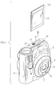
- Fig. 1 shows an instant camera having a built-in flashing device according to the present invention.
- the front of a camera body 2 is provided with a lens barrel 3 of a collapsible type, a light emitting window 4, and a light receiving window 5. These windows are used for performing automatic focusing.
- the lens barrel 3 holds a taking lens 6.
- the front of the lens barrel 3 is provided with a photometry window 7 for performing photometry of subject brightness, and a flash receiving window 8.
- a grip portion 9 is provided with a release button 10, a higher portion of which is provided with a flash emitting unit 11 of the flashing device and a viewfinder 12.
- a top face of the camera body 2 is provided with a main switch button 13, a setting button 14, an LCD 15 and an outlet 16.
- the inside of the grip portion 9 becomes a battery chamber which is loaded with a battery (not shown) being as a power source of the instant camera.
- a light emitting unit and a light receiving unit for measuring a distance are incorporated behind the light emitting window 4 and the light receiving window 5.
- a light receiving element for photometry is disposed behind the photometry window 7.
- a phototransistor 18 for automatically regulating the light is disposed behind the flash receiving window 8.
- the release button 10 When the release button 10 is depressed by half a stroke, the light for measuring a distance is emitted from the light emitting unit toward a subject. The reflected light is received by the light receiving unit to measure the subject distance. Meanwhile, subject brightness is measured by the light receiving element via the photometry window 7. Successively, the release button 10 is fully depressed. Upon this, focusing of the taking lens 6 is performed in accordance with the measured subject distance. After that, a shutter blade of a program system is operated on the basis of the measured subject brightness to expose an instant photo film 17.
- the flash light is emitted from the flash emitting unit 11 toward the subject in synchronism with the operation of the shutter blade.
- the flash light reflected by the subject is received by the phototransistor 18.
- flashing is stopped.
- the shutter blade is operated at a fixed shutter speed and a fixed stop value for flashing.
- the exposed instant photo film 17 is extruded from the outlet 16.
- a developer pod 17a of the instant photo film 17 is ruptured by a pair of development rollers provided behind the outlet 16. Owing to this, developing solution contained in the developer pod 17a is developed into the instant photo film 17. In this way, a developing process necessary for the instant photo film 17 is completed, and a photo print is obtained after a set period has passed.
- the LCD 15 displays necessary information relative to photographing, for example, the flash mode, a remaining number of the instant photo films, and a remaining amount of a battery.
- the flash mode it is possible to select either of the automatic flash mode and a flash prohibiting mode.
- flashing is automatically performed in synchronism with the operation of the shutter blade when the subject brightness is the predetermined level or less.
- the flash light is emitted from the flash emitting unit 11 toward the subject.
- flash prohibiting mode flashing is not performed without regard to the subject brightness.
- FIG. 2 partially shows a structure of the instant camera.
- a microcomputer 20 is a chip in which a CPU, an interface, an A-D converter and so forth are integrated.
- the interface performs input-output of signals and data relative to the respective sections.
- the A-D converter is described later.
- the microcomputer 20 is connected to a ROM 21, a RAM 22, an EEPROM 23 and so forth.
- the microcomputer 20 controls the whole operation of the instant camera in accordance with a sequence program stored in the ROM 21.
- the RAM 22 is utilized as a work memory in which data for executing the sequence is temporarily written.
- data D REF1 of a reference voltage described later is written at the time of manufacturing.
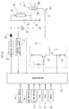
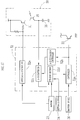
- the flashing device is constituted of a booster circuit 25, a main capacitor 26, a charging-voltage detection circuit 27, a flash discharge tube 28, trigger capacitor 29, a trigger coil 30, an IGBT (insulation-gate type bipolar transistor) 31, a light receiving circuit 32, and so forth. Flashing is controlled by the microcomputer 20.
- the booster circuit 25 is activated while a charge signal is inputted from the microcomputer 20.
- the booster circuit 25 converts a low voltage of the battery to an alternating high voltage to output it.
- the alternating voltage outputted from the booster circuit 25 is rectified by a rectifier diode 25a and is supplied to the main capacitor 26 to charge it.
- the rectifier diode 25a is arranged between the booster circuit 25 and the main capacitor 26 such that a cathode of the rectifier diode 25a is adapted to be connected with a plus side of the main capacitor 26.
- the microcomputer 20 detects a charging voltage of the main capacitor 26 on the basis of a detection voltage which is outputted from the charging-voltage detection circuit 27 connected to the main capacitor 26. When the charging voltage reaches a prescribed charging voltage, sending the charge signal is stopped to finish charging the main capacitor 26. When the charging voltage of the main capacitor 26 is lowered rather than the prescribed charging voltage due to natural discharge and so forth, the microcomputer 20 starts to send the charge signal again. In virtue of this, the charging voltage of the main capacitor 26 is substantially kept at the prescribed charging voltage.
- the prescribed charging voltage is set so as to be considerably higher than a minimum flashing voltage necessary for flashing the flash discharge tube 28.
- the reason for this is as follows. When the flash is emitted in a pulse state such as described later in detail, it is necessary for the stable flash to perform flashing in a state that the charging voltage of the main capacitor 26 is equal to the minimum flashing voltage or more.
- the flash discharge tube 28 is arranged in the flash emitting unit 11.
- One end of the flash discharge tube 28 is connected to a plus side of the main capacitor 26, and the other end thereof is connected to one end of a primary coil 30a of the trigger coil 30.
- the other end of the primary coil 30a is connected to a collector terminal of the IGBT 31.
- An emitter terminal of the IGBT 31 is grounded to be connected to a minus side of the main capacitor 26.
- a gate terminal of the IGBT 31 is connected to the microcomputer 20.
- a secondary coil 30b of the trigger coil 30 one end thereof is connected to a trigger electrode 33 provided near the flash discharge tube 28, and the other end thereof is connected to the collector terminal of the IGBT 31.
- One end of the trigger capacitor 29 is connected to the cathode of the rectifier diode 25a via a resistance 34, and the other end thereof is grounded. Moreover, the above-noted end of the trigger capacitor 29 is connected to one end of the primary coil 30a.
- the trigger capacitor 29 is charged, together with the main capacitance 26, by an output current of the booster circuit 25.
- IGBT 31 is repeatedly turned on and off in a short cycle during one exposure when the flash signal is inputted from the microcomputer 20 to the gate terminal of the IGBT. While the IGBT 31 is turned on, the flash discharge tube 28 is connected to the main capacitor 26 to emit the flash light. Since the IGBT 31 is repeatedly turned on and off, the flash discharge tube 28 repeatedly flashes in the pulse state during one exposure. In other words, the flashing device is set in an intermittent operation mode.
- stepping flash means the flash light which is emitted in the pulse state while the IGBT 31 is turned on.
- the trigger capacitor 29 lets a discharge current flow in the primary coil 30a when the IGBT 31 is turned on at the outset every exposure.
- a trigger voltage of several kV is generated in the secondary coil 30b.
- the trigger voltage is applied to the flash discharge tube 28 via the trigger electrode 33.
- the flash discharge tube 28 discharges the electric charge of the main capacitor 26 while internal insulation of the flash discharge tube 28 is broken and the IGBT 31 is turned on. In this way, the first stepping flash is performed.
- the succeeding stepping flash is performed by turning on the IGBT 31 in a state that the flash discharge tube 28 is activated owing to the last stepping flash.
- the succeeding stepping flash is performed only by turning on the IGBT 31 for connecting the flash discharge tube 28 to the main capacitor 26, without applying the trigger voltage to the flash discharge tube 28.
- the primary coil 30a of the trigger coil 30 is arranged between the flash discharge tube 28 and the main capacitor 26.
- the primary coil 30a works as a choke coil so that the light amount of the stepping flash is considerably prevented from increasing at the beginning of flashing.
- flashing is intermittently performed.
- the primary coil 30a work as the choke coil, the flash-light amount may be controlled more effectively to avoid the over-exposure.
- the choke coil may be separately provided. It is needless to say that a number of parts increases if so.
- the light receiving circuit 32 is constituted of the above-mentioned phototransistor 18 and a capacitor 35. A fixed voltage is applied to a collector terminal of the phototransistor 18. One end of the capacitor 35 is connected to an emitter terminal of the phototransistor 18, and the other end thereof is grounded. The light receiving circuit 32 outputs a charging voltage of the capacitor 35 being as a integral voltage V Cph to the microcomputer 20.
- the phototransistor 18 receives the flash light reflected by a subject, and lets a photocurrent flow in accordance with an amount of the received flash light.
- the capacitor 35 is charged by the photocurrent. As charging is performed, the charging voltage of the capacitor 35, namely the integral voltage V Cph is raised.
- the light receiving circuit 32 receives the flash light reflected by the subject to integrate the light amount. Then, the integral voltage V Cph is outputted in accordance with the integrated light amount.
- the microcomputer 20 measures the subject distance with the light emitting unit and the light receiving unit used for measuring the distance. At the same time, the microcomputer 20 measures the subject brightness with the light receiving element used for photometry. Successively, when the release button 10 is fully depressed, the microcomputer 20 actuates a shutter device 36 after focusing of the taking lens 6 has been performed in accordance with the obtained subject distance. In case the subject brightness is a predetermined level or less under the automatic flash mode, the shutter blade is operated at a shutter speed and at a stop value for flashing.
- a synchronizing signal which is a commencement signal for starting the flash, is sent from the shutter device 36 to the microcomputer 20 in synchronism with the operation of the shutter blade.
- the microcomputer 20 begins to send the flash signal to start flashing.
- the microcomputer 20 executes the A-D conversion relative to the integral voltage V Cph while flashing is performed.
- the converted integral voltage is monitored.
- the flash signal is stopped to be sent so that flashing is stopped.
- Fig. 3 shows a block diagram of the microcomputer 20.
- the microcomputer 20 works as a controller for turning on and off the IGBT 31. Besides this, the microcomputer 20 works as a light regulator together with the light receiving circuit 32.
- a controller 20a starts to send the flash signal in response to the synchronizing signal inputted from the shutter device 36.
- the IGBT 31 is turned on and off for the respective periods at the time of flashing.
- the flash signal is stopped to be sent when a stop signal is inputted. Upon this, the IGBT 31 is continuously turned off. In other words, the flashing device is set in a non-operation mode.
- the IGBT 31 is turned on while the flash signal is "H level”, namely while an on-signal is inputted.
- the IGBT 31 is turned off while the flash signal is "L level”, namely while an off-signal is inputted.
- the IGBT 31 is turned on during an on-period which is identical with a pulse width (period) T on of the on-signal.
- the IGBT 31 is turned off during an off-period which is identical with a pulse width (period) T off of the off-signal.
- commencement of sending the flash signal means commencement of outputting the on-signal and the off-signal.
- stopping the flash signal means continuously outputting the off-signal.
- the pulse width T on of the on-signal and the pulse width T off of the off-signal are fixed.
- the flash signal having a fixed cycle and a fixed duty factor is given to the IGBT 31.
- the light amount of the individual stepping flash tends to increase at the beginning of the flash, as a number of the stepping flash increases. After the light amount of the stepping flash has reached the peak, the light amount of the individual stepping flash tends to decrease. This tendency is considered to be caused by a change of an activation state in the flash discharge tube 28 and by a change of the charging voltage of the main capacitor 26, for example.
- the light amount of the individual stepping flash is changed, even if the activation state of the flash discharge tube 28 is fixed and the charging voltage of the main capacitor 26 is fixed. This phenomenon is confirmed as a result of experiment by the inventors of this application. Concretely, the light amount of the individual stepping flash decreases as the pulse width T on decreases or the pulse width T off increases. On the contrary, the light amount of the individual stepping flash increases as the pulse width T on increases or the pulse width T off decreases.
- the respective pulse widths T on and T off are properly adjusted in advance.
- the pulse width T on is adjusted to "7 ⁇ s”
- the pulse width T off is adjusted to "40 ⁇ s”.
- the stepping flash is properly performed by certain times so as to correspond to full flashing when the shutter blade is operated.
- the stepping flash is performed in "3 ms" by times corresponding to full flashing.
- An A-D conversion controller 20b monitors a signal level of the flash signal to control sampling performed by an A-D converter 20c which is incorporated in the microcomputer 20. When the flash signal is changed from "H level” to "L level", the A-D conversion controller 20b instructs the A-D converter 20c to perform sampling.
- the integral voltage V Cph is inputted from the light receiving circuit 32.
- the A-D converter 20c performs sampling of the integral voltage V Cph upon receiving the instruction of sampling. An obtained voltage value is digitally converted to integral voltage data D Cph and is sent to a judging section 20d.
- the judging section 20d compares the integral voltage data D Cph with data D REF1 of the reference voltage whenever the integral voltage data D Cph is inputted. When the data D Cph is equal to the data D REF1 or more, the stop signal is sent to the controller 20a. Judging sequence is executed from the commencement of sampling performed by the A-D converter 20c to the judgement by the judging section 20d. This sequence is completed within the duration that the flash signal is "L level".
- sampling by the A-D converter 20c may be performed during the stepping flash.
- the integral voltage V Cph is sampled during an increase thereof so that the sampled integral voltage V Cph becomes smaller than the integral voltage V Cph obtained after completion of the stepping flash.
- the extra stepping flash is emitted.
- the reference voltage data D REF1 is determined such that the integral voltage V Cph outputted from the light receiving circuit 32 is equal to the voltage data converted by the A-D converter 20c at a juncture that flashing is performed and a normal exposure amount is given to the instant photo film 17. Further, the reference voltage data D REF1 is determined, taking account an error of the light receiving circuit 32. Accordingly, the instant camera has the reference voltage data D REF1 being respectively different.
- the stop signal is sent to the controller 20a.
- the flash signal is stopped to be sent so that the succeeding stepping flash is prohibited and flashing for one exposure is finished.
- the microcomputer 20 does not need to integrate the light amount.
- the A-D converter 20c may be externally attached.
- the circuit of the microcomputer 20 merely needs to be changed without altering its producing process. In this case, the producing cost is hardly increased.
- the integral voltage data D Cph is smaller than the reference voltage data D REF1 . Even if a difference between them is small, the next stepping flash is sometimes performed to cause the over-exposure. Especially, at the beginning of flashing wherein the light amount of the stepping flash tends to increase, there is a high possibility to cause the great over-exposure. In order to prevent this problem, even if the integral voltage data D Cph does not reach the reference voltage data D REF1 , flashing may be finished in case the difference is small, for example, in case the integral voltage data D Cph reaches 95% of the reference voltage data D REF1 .
- a collapsing mechanism which is not shown is actuated to protrude the lens barrel 3 toward the photographic position. Then, the instant camera is set in a waiting state capable of photographing. In this state, the microcomputer 20 monitors the charging voltage of the main capacitor 26 on the basis of the detection voltage outputted from the charging-voltage detection circuit 27. When the charging voltage of the main capacitor 26 does not reach the prescribed charging voltage, the booster circuit 25 is activated to perform charging.
- the charging voltage of the main capacitor 26 is substantially kept at the prescribed charging voltage, and a flashable state is always set. Meanwhile, the trigger capacitor 29 is simultaneously charged when the main capacitor 26 is charged. Incidentally, when the flash prohibiting mode is selected by handling the setting button 14, charging may be stopped despite the charging voltage of the main capacitor 26.
- a subject distance is measured with the light emitting unit and the light receiving unit for measuring the distance.
- subject brightness is measured with the light receiving element for photometry.
- the reference voltage data D REF1 is read from the EEPROM 23 to be set in the judging section 20d.
- the shutter device 36 is actuated to operate the shutter blade at the shutter speed and the stop for flashing.
- the synchronizing signal is inputted into the controller 20a of the microcomputer 20.
- the controller 20a starts to send the flash signal in response to the inputted synchronizing signal.
- the flash signal of "H level”, namely the on-signal is inputted into the IGBT 31, this IGBT 31 is turned on.
- a period during which the IGBT 31 is turned on is identical with the pulse width T on of the on-signal.
- the charged trigger capacitor 29 lets the discharge current flow in the primary coil 30a.
- the trigger voltage generated at the secondary coil 30b is applied to the flash discharge tube 28.
- the internal insulation of the flash discharge tube 28 is broken. Then, while the IGBT 31 is turned on, the electric charge of the main capacitor 26 is discharged to emit the flash light. The flash light emitted from the flash discharge tube 28 is radiated toward the subject by the flash emitting unit 11. In this way, the first stepping flash is performed.
- the flash light of the first stepping flash is reflected by the subject, and a part thereof enters the phototransistor 18 through the flash receiving window 8. Upon this, the phototransistor 18 lets the photocurrent corresponding to an incidence-light amount flow. By this photocurrent, the capacitor 35 is charged. Thus, the integral voltage V Cph is raised.
- the flash signal is set to the "L level".
- the IGBT 31 is turned off to cut the connection between the flash discharge tube 28 and the main capacitor 26. Upon this, emitting the flash light is stopped, and the first stepping flash is finished.
- the A-D conversion controller 20b sends the instruction of sampling to the A-D converter 20c. Based on the instruction, the A-D converter 20c performs sampling of the integral voltage V Cph outputted from the light receiving circuit 32. Further, the A-D converter 20c converts the integral voltage V Cph to the integral voltage data D Cph and sends it to the judging section 20d.
- this judging section 20d compares the integral voltage data D Cph with the reference voltage data D REF1 to judge the relationship between them. In this judgment, when the integral voltage data D Cph is equal to the reference voltage data D REF1 or more, the judging section 20d sends the stop signal to the controller 20a to stop the flash signal. However, when the integral voltage data D Cph is smaller than the reference voltage date D REF1 , the stop signal is not sent.
- the judging sequence is executed from the commencement of sampling performed by the A-D converter 20c to the judgment performed by the judging section 20d. This sequence is completed within the period (pulse width) T off of the off-signal, and it is decided whether the stop signal is sent or not by the timing for inputting the second on-signal into the IGBT 31.
- the stop signal is not inputted into the controller 20a.
- the flash signal is set to the "H level” again and the second on-signal having the pulse width T on is inputted into the IGBT 31.
- the flash discharge tube 28 which is kept in a state activated by the first stepping flash, is connected to the main capacitor 26.
- the electric charge of the main capacitor 26 is discharged again in the flash discharge tube 28, and the flash light is emitted from the flash discharge tube 28 to start the second stepping flash.
- the flash signal is set to the "L level" after the second on-signal and the second off-signal is inputted into the IGBT 31. Owing to this, the IGBT 31 is turned off to finish the second stepping flash.
- the capacitor 35 is charged.
- the integral voltage V Cph is raised by an extent corresponding to the incidence-light amount of the instant photo film 17.
- the integral voltage V Cph is set to a value corresponding to the incidence-light amount of the instant photo film 17 relative to the first and second stepping flashes. Strictly speaking, the capacitor 35 discharges during an interval between the first and second stepping flashes so that the integral voltage V Cph is slightly lowered.
- the flash signal is set to the "L level" after secondarily turning on the IGBT 31, sampling is performed by the A-D converter 20c similarly to the foregoing.
- the integral voltage V Cph is converted to the integral voltage data D Cph to be sent to the judging section 20d.
- the judgement is performed by the judging section 20d.
- the stop signal is sent to the controller 20a to stop the flash signal.
- the integral voltage data D Cph is smaller than the reference voltage data D REF1 , the stop signal is not sent.
- the flash signal is continued to be sent until the integral voltage data D Cph reaches the reference Voltage data D REF1 .
- the third stepping flash and the succeeding stepping flash are performed in order.
- the stop signal is sent at that time to stop the flash signal.
- the judging sequence is executed just after the Nth stepping flash has been performed by the Nth on-signal and while the Nth off-signal is inputted into the IGBT 31.
- the stop signal is sent from the judging section 20d to the controller 20a at that time.
- the controller 20a continuously outputs the off-signal as the Nth off-signal.
- the (N+1)th stepping flash and the succeeding stepping flash are not performed so that flashing of one exposure is finished.
- the instant photo film 17 is exposed by the flash light emitted in the stepping flashes of N times.
- the normal exposure amount is almost applied to the instant photo film 17.
- the exposed instant photo film 17 is extruded from the outlet 16. At the time of extrusion, developing solution is developed inside the instant photo film 17. In virtue of this, a necessary process for developing the instant photo film 17 is completed, and a photo print is obtained after a predetermined period has passed.
- the stepping flash is repeated through the one-exposure period.
- successive flashing may be performed after the stepping flash has been repeated at the beginning of flashing.
- a constituting member which is substantially identical with that of the above embodiment is denoted by the same reference numeral, and detailed explanation thereof is omitted.
- the controller 20a gives a predetermined number of the on-signals to the IGBT 31 so as to repeat the stepping flash. After that, the flash signal is continuously set to the "H level" so as to successively perform flashing. In other words, the on-signal is continuously inputted into the IGBT 31 to successively turn on the IGBT 31. Owing to this, successive flash is performed after a predetermined period has passed from the commencement of flashing. In other words, the flashing device is set in a continuous operation mode.
- the judging sequence is executed just after the stepping flash whenever the stepping flash is performed. Meanwhile, while the flash signal is continuously set to the "H level", the A-D converter 20c is controlled by the A-D conversion controller 20c to perform sampling of the integral voltage V Cph at fixed intervals. The judging section 20d makes the judgment every sampling of the integral voltage V Cph .
- the judging sequence is executed from sampling of the integral voltage V Cph to the judgment by the judging section 20d. This sequence is repeated at fixed intervals.
- the flash signal is set to the "L level" to finish flashing.
- the integral voltage data D Cph reaches the reference voltage data D REF1 while the stepping flash is repeated, flashing is finished at that time. Thus, the successive flash is not performed.
- Timing for changing the stepping flash to the successive flash is determined based on a changing pattern of the flash-light amount and so forth. The timing is determined as a period from the commencement of flashing until a juncture that an increase of the exposure amount becomes gradual.
- the light amount of the individual stepping flash tends to increase, as the number of the stepping flashes increases at the beginning of flashing. After that, the light amount of the individual stepping flash tends to decrease. Under such a tendency, an exposure value (EV) of the flash light applied to the instant photo film 17 suddenly increases at the beginning of flashing. After the light amount of the stepping flash has reached the peak, namely in the latter half of flashing, although the exposure value increases, an increasing rate thereof lowers. Thus, the exposure value is adapted to gradually increase.
- the electric charge of the main capacitor 26 is almost discharged by the flash discharge tube 28.
- the main capacitor 26 having a smaller capacity in comparison with the case for merely performing the stepping flash.
- the timing for changing to the successive flash such that changing to the successive flash is performed when the charging voltage of the main capacitor 26 is equal to the minimum flashing voltage of the flash discharge tube 28 or more. It is necessary, in order to perform the stable successive flash, that the charging voltage of the main capacitor 26 is equal to the minimum flashing voltage of the flash discharge tube 28 or more. Meanwhile, a delay of the timing for stopping the flash is changed in accordance with an execution period and a cycle of the judging sequence. Moreover, the increase of the exposure value is also changed in accordance with the delay of the timing. Thus, it is necessary to determine the timing for changing from the stepping flash to the successive flash so as not to be affected by the increase of the exposure value, taking account of the execution period and the cycle of the judging sequence. Of course, in view of the delay of the timing, the reference voltage data D REF1 used in the successive flash may be adapted to be smaller than that in the stepping flash.
- passage of the set period for changing from the stepping flash to the successive flash is detected by utilizing the predetermined cycle of the flash signal and upon completion of sending the predetermined number of the on-signals.
- the period from the commencement of flashing may be measured by a timer, and changing to the successive flash may be performed when the measured period has reached a prescribed period.
- the timing for changing to the successive flash may be determined on the basis of a number of the sent on-signals, namely a frequency of turning on the IGBT 31.
- Fig. 7 is a block diagram of the microcomputer 20 showing an embodiment in which changing to the successive flash is performed based on the integral voltage data D Cph .
- a circuit of the flashing device is identical with the circuit shown in Fig. 2.
- a member in Fig. 7 which is substantially identical with that in Fig. 3 is denoted by the same reference numeral.
- the microcomputer 20 performs changing to the successive flash on the basis of the integral voltage data D Cph
- the other points are similar to the embodiment shown in Fig. 6, for example, relative to the timing for sampling the integral voltage V Cph and so forth.
- a pulse-width controller 20e calculates a difference between the current integral voltage data D Cph and the last integral voltage data D Cph .
- the current integral voltage data D Cph is outputted from the A-D converter 20c every stepping flash.
- the last integral voltage data D Cph has been outputted at the last time.
- the pulse-width controller 20e instructs the controller 20a to continuously output the on-signal.
- the controller 20a sets the flash signal to the "H level" to perform the successive flash until the stop signal is inputted from the judging section 20d.
- changing to the successive flash is performed based on the increase of the integral voltage data D Cph .
- this is not exclusive.
- Changing to the successive flash may be performed based on, for example, a ratio of the current integral voltage data D Cph to the last integral voltage data D Cph , a size of the integral voltage data D Cph , a difference between the increases of the current integral voltage data D Cph and the last integral voltage data D Cph , and a ratio thereof.
- Fig. 8 shows an embodiment in which the pulse width Ton, namely the on-period of the IGBT 31 is changed, instead of changing to the successive flash on the basis of the integral voltage data D Cph .
- the on-signal whose pulse width Ton is relatively narrow at the beginning of the flash is inputted into the IGBT 31.
- the integral voltage data D Cph is monitored by the pulse-width controller 20e similarly to the embodiment shown in Fig. 7.
- the pulse width Ton of the on-signal is widened in comparison with that of the beginning of flashing.
- the on-period (the pulse width Ton) is changed in two steps.
- the on-period may be changed in three steps or more. Otherwise, the on-period may be successively changed.
- the pulse width Toff of the off-signal may be shortened to shorten the off-period of the IGBT 31.
- both of the on-period and the off-period may be changed.
- the successive flash may be performed by continuously outputting the on-signal after the flash signal has been changed so as to extend the on-period, such as shown in Fig. 9.
- the successive flash may be performed by continuously outputting the on-signal after the flash signal has been changed so as to shorten the off-signal.
- the on-period and the off-period of the IGBT 31 are changed based on the integral voltage data D Cph .
- the on-period and the off-period may be changed based on a period from the commencement of flashing, and based on a number of turning on the IGBT 31. Otherwise, it is possible to change to the successive flash after the on-period and the off-period have been changed.
- Figs. 10 through 13 show an embodiment in which a photocurrent flowing in the light receiving element is converted to a voltage by a resistance, instead of integrating the light amount with the capacitor included in the light receiving circuit. Based on the obtained voltage, the light amount is integrated by an operation of the microcomputer.
- a constituting member which is substantially identical with that of the first embodiment is denoted by the same reference numeral, and explanation thereof is omitted.
- the light receiving circuit 41 is constituted of the phototransistor 18 and a resistance 42.
- a fixed voltage is inputted into a collector terminal of the phototransistor 18.
- the resistance 42 is provided for converting a photocurrent flowing during the stepping flash to a light-reception voltage corresponding thereto.
- One end of the resistance 42 is connected to an emitter terminal of the phototransistor 18, and the other end thereof is grounded.
- the photocurrent corresponding to the light amount received by the phototransistor 18 flows in the resistance 42, and a voltage corresponding to the photocurrent is generated between both ends of the resistance 42.
- the light receiving circuit 41 outputs the generated voltage to the microcomputer 43 as a light-reception voltage V Rph .
- A-D conversion is carried out relative to the light-reception voltage V Rph obtained during the stepping flash.
- the microcomputer 43 performs a predetermined integral operation to integrate the flash-light amount reflected by a subject.
- the flash signal is stopped to finish flashing.
- Fig. 11 shows a block diagram of the microcomputer 43.
- a controller 43a is identical with the controller 20a of the first embodiment shown in Fig. 3.
- the controller 43a starts to send the flash signal in response to the input of the synchronizing signal and stops sending the flash signal upon the input of the stop signal.
- An A-D conversion controller 43b monitors a signal level of the flash signal. When a predetermined period passes after the flash signal has been changed from the "L level” to the "H level", the A-D conversion controller 43b instructs a A-D converter 43c to perform sampling. Upon this, sampling is executed during the stepping flash.
- the light-reception voltage V Rph from the light receiving circuit 41 is inputted to the A-D converter 43c.
- the A-D converter 43c performs sampling of the light-reception voltage V Rph upon the instruction from the A-D conversion controller 43b.
- the sampled one is digitally converted to light-reception voltage data D Rph and is sent to an integrating section 43d.
- the integrating section 43d integrates the inputted light-reception voltage data D Rph by a predetermined integral operation.
- the flash-light amount received by the phototransistor 18 is integrated, including the stepping flash from which the inputted light-reception voltage data D Rph is obtained.
- integral voltage data D RS is calculated and is sent to a judging section 43e.
- the judging section 43e compares the integral voltage data D RS with a reference voltage data D REF2 whenever the integral voltage data D RS is inputted.
- the stop signal is sent to the controller 20a.
- the reference voltage data D REF2 is predetermined in view of an error of the light receiving circuit 32 such that the reference voltage data D REF2 is adapted to be equal to the integral voltage data D RS obtained from the integrating section 43d, when flashing is performed and the normal exposure amount is given to the instant photo film 17.
- the reference voltage data D REF2 is written in the EEPROM 23.
- the reference voltage data D REF2 is different relative to the respective instant cameras.
- the judging sequence is executed from sampling of the light-reception voltage V Rph to the judgment by the judging section 43e. This sequence is executed every stepping flash and is completed within a term that the flash signal is set to the "L level". Thus, before the next on-signal is inputted into the IGBT 31, it is decided whether the stop signal is sent or not.
- the light amount is integrated based on the light-reception voltage V Rph obtained during the stepping flash
- a relationship between the integral voltage data D RS and an actual exposure amount is sometimes varied due to the sampling timing in the individual stepping flash, even if the stepping flash is performed under the similar condition.
- the reason of this is considered as follows.
- strength of the flash light is gradually increased after turning on the IGBT 31, and is suddenly changed to zero when the IGBT 31 is turned off after the strength of the flash light has reached the peak.
- the sampling timing of the light-reception voltage V Rph is fixed in the respective stepping flashes, and sampling is adapted to be performed when the strength of the flash light has reached the peak, for example. Based on this timing, is adjusted and determined the reference voltage data D REF2 used for controlling the stop of flashing. The timing that the strength of the flash light reaches the peak can be experimentally found as a delay period which is delayed after sending the off-signal to the IGBT 31. Meanwhile, the light-reception voltage data D Rph may be weighted in accordance with the sampling timing to calculate the integral voltage data D RS .
- the integral voltage data D RS is less than the reference voltage data D REF2 and the difference between them is small, the over-exposure is sometimes caused by performing the next stepping flash.
- the integral voltage data D RS is less than the reference voltage data D REF2 , flashing may be finished when the difference between them is small.
- the reference voltage data D REF2 is read from the EEPROM 23 and is set to the judging section 43e.
- the synchronizing signal is inputted into the controller 43a of the microcomputer 43 in synchronism with the operation of the shutter blade. Then, as shown in Figs. 12 and 13, when the flash signal is sent from the controller 43a in response to the input of the synchronizing signal, the IGBT 31 is turned on and off to start the stepping flash.
- the first stepping flash is started by firstly turning on the IGBT 31. After that, when the IGBT 31 is turned off, the first stepping flash is finished.
- the flash light emitted during the first stepping flash is reflected by a subject, and a part thereof enters the phototransistor 18.
- a photocurrent flows in the resistance 42.
- the photocurrent is converted to the corresponding light-reception voltage V Rph by the resistance 42 to be sent from the light receiving circuit 41.
- the A-D conversion controller 43b instructs the A-D converter 43c to perform sampling after a proper delay.
- the light-reception voltage V Rph outputted from the light receiving circuit 41 is sampled by the A-D converter 43c during the first stepping flash.
- the sampled one is converted to the light-reception voltage data D Rph to be sent to the integrating section 43d.
- the integrating section 43d integrates the flash-light amount received by the phototransistor 18 during the first stepping flash.
- the flash-light amount is integrated by applying a predetermined operation formula.
- the integral voltage data D RS is calculated. In other words, the integral voltage data D RS is calculated in accordance with the exposure amount of the instant photo film 17 given by the first stepping flash.
- the integral voltage data D RS is sent to the judging section 43e.
- this judging section 43e compares the integral voltage data D RS with the reference voltage data D REF2 to judge a relationship between them. In this judgement, when the integral voltage data D RS is equal to the reference voltage data D REF2 or more, the stop signal is sent to the controller 43a to stop the flash signal. However, when the integral voltage data D RS is less than the reference voltage data D REF2 , the stop signal is not sent.
- the judgement by the judging section 43e is completed within the period (pulse width) Toff of the off-signal. Before the second on-signal is started to be inputted into the IGBT 31, it is decided whether the stop signal is sent or not.
- the flash signal is set to the "H level” again after the period T OFF has passed from the point that the flash signal is lastly set to the "L level”. Then, the second on-signal having the pulse width T ON is inputted into the IGBT 31. Upon turning on the IGBT 31, the second stepping flash is performed.
- the phototransistor 18 Similarly to the first stepping flash, a part of the flash light reflected by the subject enters the phototransistor 18 during the second stepping flash. In accordance with the incidence-light amount, the photocurrent flows.
- the light-reception voltage V Rph corresponding to the photocurrent is outputted from the light receiving circuit 41.
- the light-reception voltage V Rph is converted to the light-reception voltage data D Rph by the A-D converter 43c to be sent to the integrating section 43d.
- the integrating section 43d carries out the integral operation by using the last operation result, and calculates the integral voltage data D RS corresponding to the integral amount in which the integral amounts of the first and second stepping flashes are added.
- the integral voltage data D RS is sent to the judging section 43e to perform the judgement.
- sending the flash signal is continued to perform the stepping flash until the integral data D RS reaches the reference data D REF2 .
- sending the flash signal is stopped by the stop signal outputted from the judging section 43e, and flashing of one exposure is finished.
- flashing of one exposure is finished at that time.
- the light amount is integrated based on the light-reception voltage V Rph obtained during the stepping flash, and the integral amount is checked to determine whether the next stepping flash is performed or not.
- the A-D converter 43c and the microcomputer 43 adopted in the present invention have a comparatively slow processing speed and are low in price, it is possible to control the flash-light amount with accuracy so that the over-exposure may be prevented. Moreover, it is possible to control the flash-light amount by a small number of parts without using a voltage controller and so forth.
- Fig. 14 shows an example in which the stepping flash is repeated, similarly to the embodiment shown in Fig. 6, in the circuit structure shown in Fig. 10.
- flashing is successively performed.
- the stepping flash is repeated by giving a predetermined number of the on-signals to the IGBT 31, the light-reception voltage V Rph is sampled during the stepping flash to execute the judging sequence.
- the flash signal is continuously set to the "H level", namely while the flashing is successively performed, the light-reception voltage V Rph is sampled at the fixed intervals to execute the judging sequence.
- the integral voltage data D RS reaches the reference voltage data D REF2
- the flash signal is set to the "L level" so that flashing is finished.
- a period from the commencement of flashing may be measured by a timer, and when the measured period has reached a predetermined period, changing to the successive flash may be performed.
- the timing for changing to the successive flash may be determined based on a number of turning on the IGBT 31.
- Fig. 15 is a block diagram of the microcomputer and shows an embodiment in which changing to the successive flash is performed based on the integral voltage data D RS .
- the circuit of the flashing device is identical with the circuit shown in Fig. 10.
- a member which is substantially identical with that in Fig. 11 is denoted by the same reference numeral.
- the sampling timing of the integral voltage V Rph and so forth are similar to the embodiment shown in Fig. 14.
- a pulse-width controller 43f obtains a difference between the current integral voltage data D RS and the last integral voltage data D RS .
- the current integral voltage data D RS is outputted from the integrating means 43d while the stepping flash is repeated.
- the controller 43a is instructed to continuously output the on-signal. Owing to this, when an increase of the integral voltage data D RS , namely an increase of the exposure amount of the flash light becomes gradual, the on-signal is continuously outputted from the controller 43a to change to the successive flash.
- the A-D conversion controller 43b controls the A-D converter 43c so as to perform sampling of the integral voltage V Cph at a fixed intervals.
- changing to the successive flash may be performed based on a ratio of the current integral voltage date D RS to the last integral voltage data D RS , a size of the integral voltage data D RS , a difference between the increases of the current integral voltage data D RS and the last integral voltage data D RS , and a ratio thereof.
- a ratio of the current integral voltage date D RS to the last integral voltage data D RS a size of the integral voltage data D RS
- a difference between the increases of the current integral voltage data D RS and the last integral voltage data D RS a ratio thereof.
- the changing timing from the stepping flash to the successive flash is determined in view of the execution time and the cycle of the judging sequence so as not to be substantially affected by the increase of the exposure value caused by the delay of the flash stopping.
- changing to the successive flash may be performed based on the integral voltage data D RS , the period from the commencement of flashing, and the number of turning on the IGBT 31. Moreover, changing to the successive flash may be performed by changing at least one of on-period and the off-period of the IGBT 31. Further, changing to the successive flash may be performed after the on-period and the off-period have been changed.
- the light-reception voltage V Rph is sampled to integrate the light amount
- the sampling timing in accordance with the change of the on-period and the off-period, in order to fix the relationship between the light-reception voltage V Rph and the obtained exposure amount.
- the on-signal and the off-signal having the fixed pulse widths T ON and T OFF are inputted at the beginning of flashing.
- the stepping flash is sometimes not performed and sometimes becomes unstable. It is possible to make the stepping flash stable by widening the pulse width T ON of the flash signal for firstly turning on the IGBT 31, for example, up to about "20 ⁇ s".
- the normal exposure amount is obtained by the flash light.
- the reference voltage data corresponding to the exposure amount relative to the normal exposure amount is prepared and is selected in accordance with designation of the exposure amount, it is possible to adjust the flash-light amount so as to correspond to the exposure amount relative to the normal exposure amount.
- Figs. 16 through 21 show an embodiment of the flashing device in which a light-regulation level can be easily adjusted. Except the following, the circuit structure and the operation are similar to those of the first embodiment.
- the identical constituting member is denoted by the same reference numeral, and the description thereof is omitted.
- an exposure correction mode can be selected besides the flashing mode and so forth.
- the selected exposure correction mode is displayed on the LCD 15.
- the exposure correction mode it is possible to select any one of a "normal mode” in which a photo print has normal density gradation, a "light mode” in which a photo print has light density gradation, and a “dark mode” in which a photo print has dark density gradation.
- exposure correction of +2/3 EV and -2/3 EV for example, is performed relative the normal mode.
- the exposure correction is performed by changing a shutter speed and a stop value when the flash light is not emitted. Meanwhile, when the flash light is emitted, the exposure correction is performed by changing the flash-light amount under a condition that the shutter speed and the stop value are fixed.
- Reference voltage data D N , D L and D D respectively corresponding to the normal mode, the light mode and the dark mode are written in the EEPROM 23 at the time of manufacturing.
- a ratio Ra used for adjusting the photosensitivity and commonly used for the respective modes are written in the EEPROM 23 at the time of manufacturing.
- the reference voltage data D N , D L and D D are for regulating a light level in accordance with the exposure correction mode in photographing.
- the data D N , D L and D D are predetermined based on the photosensitivity of the designed light receiving circuit, and are common to the respective instant cameras.
- the reference voltage data D L and D D of the light mode and the dark mode are expressed such as the following formulas 1 ⁇ and 2 ⁇ by using the reference voltage data D N of the normal mode.
- D L D N ⁇ 2 dL 1
- D D D N ⁇ 2 dD 2
- the value "dL” and the value “dD” are differences of the respective exposure values (EV) in the light mode and the dark mode relative to the normal mode.
- the dL is equal to +2/3 and the dD is equal to -2/3.
- any one of the reference voltage data for example only the reference voltage data D N used for the normal mode may be written in the EEPROM 23.
- calculation may be performed by the microcomputer of the instant camera to obtain them, using the reference voltage data D N of the normal mode.
- the ratio Ra is used for adjusting the photosensitivity of a light receiving circuit 50.
- the photosensitivity of the light receiving circuit 50 is adjusted by changing the ratio Ra to make the light-regulation level proper.
- the ratio Ra is determined relative to the respective instant cameras at the time of manufacturing.
- the light receiving circuit 50 is constituted of the phototransistor 18, the capacitor 35, and a transistor 51 used for adjusting the sensitivity.
- this transistor 51 NPN type is used.
- a fixed voltage is supplied to an emitter terminal of the transistor 51 by a power-supply circuit.
- a collector terminal of the transistor 51 is connected to the collector terminal of the phototransistor 18.
- a base terminal of the transistor 51 is connected to a microcomputer 52 so that the transistor 51 is turned on and off by the microcomputer 52.
- An emitter terminal of the phototransistor 18 is connected to one end of the capacitor 35, and the other end of the capacitor 35 is grounded.
- the transistor 51 is repeatedly turned on and off while flashing is performed.
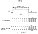
- the photosensitivity of the light receiving circuit 50 is adjusted by changing a ratio of the on-period Ts to a cycle T for turning on and off the transistor 51.
- the microcomputer 52 controls the booster circuit 25, the charging-voltage detection circuit 27 and the IGBT 31, and monitors the integral voltage V Cph obtained from the light receiving circuit 50. Besides these, the microcomputer 52 turned on and off the transistor 51.
- Fig. 17 shows a block diagram of the microcomputer 52.
- a controller 52a, an A-D conversion controller 52b and an A-D converter 52c have similar functions to the controller 20a, the A-D conversion controller 20b and the A-D converter 20c of the first embodiment shown in Fig. 3.
- the A-D converter 52c linearly converts the integral voltage V Cph to the integral voltage data D Cph .
- any one of the reference voltage data D N , D L and D D corresponding to the exposure correction mode selected by the setting button is set to a judging section 52d as reference voltage data D REF3 .
- the judging section 52d compares the integral voltage data D Cph with the reference voltage data D REF3 whenever the integral voltage data D Cph is inputted. When the former is equal to the latter or more, the stop signal is sent to the controller 52a.
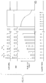
- a switching controller 52e outputs a switching signal to the transistor 51. As shown in Fig. 18, the switching controller 52e outputs the switching signal of which signal level is changed at a fixed cycle T. Moreover, the switching controller 52e outputs the switching signal such that a ratio of a period (Ts) outputting the "L level" to the cycle T of the switching signal is equal to the ratio Ra written in the EEPROM 23.
- the transistor 51 is turned on while the switching signal is set to the "L level”, and is turned off while the switching signal is set to the "H level”.
- the transistor 51 is turned on and off at the fixed cycle T.
- a ratio of the on-period Ts to the cycle T is equal to the ratio Ra written in the EEPROM 23.
- the cycle T of the switching signal is set so as to be sufficiently shorter than the on-period T ON during which the IGBT 31 is turned on by one time.
- the transistor 51 is turned on and off by several times.
- the transistor 51 is repeatedly turned on and off, and the photocurrent flows from the phototransistor 18 only for the on-period during which the transistor 51 is turned on.
- the whole light amount received by the phototransistor 18 during the individual stepping flash only the light amount corresponding to the ratio Ra is converted to the photocurrent to be supplied to the capacitor
- the light receiving circuit 50 has the photosensitivity of 70 % relative to the photosensitivity which is set at the time of continuously turning on the transistor 51.
- the ratio Ra is determined at the time of manufacturing and is written in the EEPROM 23.
- flashing is performed in a state that the switching signal is generated by using any ratio Ra T for testing.
- the reference voltage data D N for the normal mode is used as the reference voltage data D REF3 , and flashing is stopped by an automatic light regulating function.
- the exposure value EV T obtained by flashing is measured by an adjusting device.
- the ratio Ra being used is calculated at the time of photographing in accordance with the following formula 3 ⁇ .
- the ratio Ra may be easily determined so that adjustment is easily performed.
- the reference voltage data D N for the normal mode is used as the reference voltage data D REF3 .
- the reference voltage D L and D D for the light mode and the dark mode. Otherwise, it is possible to use other voltage data.
- instead of the exposure value EV N in the foregoing formula 3 ⁇ is used an exposure value corresponding to the voltage data used as the reference voltage data D REF3 .
- the instant camera into which the flashing device and so forth are incorporated is sent to a step for adjusting the light regulation level.
- the microcomputer 52 of the instant camera is connected to an adjusting device which is not shown.
- electric power is supplied from the adjusting device to the instant camera so that the instant camera is set in a operatable state.
- the instant camera connected to the adjusting device is kept in a position that the flash emitting unit 11 and the flash receiving window 8 thereof face a test reflector having a predetermined reflectance.
- the flash emitting unit 11 and the flash receiving window 8 are positioned so as to keep an interval and an angle which are predetermined and fixed relative to the test reflector.
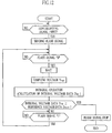
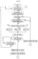
- a sequence for determining the ratio Ra is executed such as schematically shown in Fig. 19.
- the reference voltage data D N , D L and D D for the respective exposure correction modes are written in the EEPROM 23 at the outset.
- the reference voltage data D N , D L and D D are utilized at the time of normal photographing.
- the reference voltage data D N , D L and D D may be written in the EEPROM 23 in advance.
- the booster circuit 25 is activated via the microcomputer 52 upon an instruction from the adjusting device. Owing to this, the main capacitor 26 is charged up to the prescribed charging voltage. At the same time, the trigger capacitor 29 is charged. Meanwhile, the reference voltage data D N is read from the EEPROM 23 as the reference voltage data D REF3 compared with the integral voltage data D Cph . This reference voltage data D N is set in the judging section 52d. Further, the test ratio Ra T for testing is set in the switching controller 52e from the adjusting device. As to the test ratio Ra T , a value "1.0" is set in the switching controller 52e. Incidentally, the test ratio Ra T may be other value.
- an exposure meter of the adjusting device is set in an operatable state.
- a light receiving portion of the exposure meter is provided, for example, on the test reflector to receive the flash light. Based on the received light amount, the exposure value EVT by the flash light is outputted.
- the adjusting device After operating the exposure meter, the adjusting device sends an instruction for flashing to the microcomputer 52. Upon receiving the instruction, the microcomputer 52 starts outputting the switching signal from the switching controller 52e. At this time, since the value "1.0" is set in the switching controller 52e as the test ratio Ra T , the switching signal continuously kept at the "L level” is inputted into the photosensitivity adjusting transistor 51. Thus, the transistor 51 is continuously turned on.
- the microcomputer 52 starts outputting the flash signal from the controller 52a. Upon this, flashing is started and the stepping flash is repeatedly performed. The flash light emitted during the individual stepping flash is reflected by the test reflector, and a part thereof enters the phototransistor 18 through the flash receiving window 8.
- the photosensitivity adjusting transistor 51 is continuously turned on so that the phototransistor 18 allows the photocurrent to flow in accordance with the incidence flash-light amount. By this photocurrent, the capacitor 35 is charged. Owing to this, the integral voltage V Cph is raised.
- the integral voltage V Cph is sampled by the A-D converter 52c just after the stepping flash.
- the obtained integral voltage data D Cph is compared with the reference voltage data D REF3 (the reference voltage data D N ) by the judging section 52d.
- the stop signal is sent to the controller 52a.
- the judging sequence is executed from sampling by the A-D converter 52c to the judgement by the judging section 52b. This sequence is completed within a period that the IGBT 31 is turned off.
- the stop signal is sent from the judging section 52d to the controller 52a at that time.
- the controller 52a continuously sets the flash signal to the "L level".
- the exposure meter of the adjusting device receives a part of the flash light while the stepping flash is performed.
- the exposure meter outputs the exposure value EV T corresponding to the whole amount of the received light.
- the light amount is integrated under a condition that the ratio Ra T is equal to "1.0", namely the photosensitivity of the light receiving circuit 50 is 100 %.
- the exposure value EV T obtained from the exposure meter is the value in the case that the stepping flash has been performed until the integral voltage data D Cph reaches the reference voltage data D N for the normal mode.
- the exposure value EV T is sent to an arithmetic unit of the microcomputer or the like provided in the adjusting device.
- the arithmetic unit applies the exposure value EV T , the exposure value EV N corresponding to the normal mode, and the test ratio Ra T to the forgoing formula 3 ⁇ to calculate the ratio set in the flashing device.
- the calculated ratio Ra is sent from the adjusting device to the microcomputer 52, and is written in the EEPROM 23 by the microcomputer 52.
- the ratio Ra being a half value of the test ratio Ra T is written in the EEPROM 23 to be used at the time of photographing.
- the photosensitivity of the light receiving circuit 50 in the case of using the test ratio Ra T is twice relative to the proper photosensitivity of the light receiving circuit 50 in the case of using the set reference voltage data D N , D L and D D . This means that the proper photosensitivity is obtained if the ratio Ra used for photographing is set to a half value of the test ratio Ra T and the photocurrent supplied to the capacitor 35 is reduced to half.
- the exposure value EV N is equal to 11 EV and the exposure value EV T is equal to 10 EV
- the ratio Ra whose value is 0.5 is written in the EEPROM 23. This is used at the time of normal photographing.
- the instant camera in which the ratio Ra is written in the EEPROM 23 is shipped after incorporating the remaining parts and having a predetermined examination.
- the exposure correction mode selected by the setting button 14 is successively checked when the subject brightness is equal to the predetermined level or less. Then, the reference voltage data corresponding to the selected exposure correction mode is read from the EEPROM 23 by the microcomputer 52.
- the reference voltage data D N for the normal mode is read from the EEPROM 23 and is set in the judging section 52d as the reference voltage data D REF3 .
- the ratio Ra is read from the EEPROM 23 and is set in the switching controller 52e.
- the switching signal is started to be sent from the switching controller on the basis of the ratio Ra.
- the transistor 51 for adjusting the sensitivity is repeatedly turned on and off.
- a ratio of the on-period Ts to the cycle T for turning on and off the transistor 51 is identical with the ratio Ra determined at the time of manufacturing.
- the ratio Ra is 1.0, the transistor 51 is continuously turned on.
- the shutter device 36 is activated to operate the shutter blade at the shutter speed and the stop value for flashing.
- the synchronizing signal is inputted into the microcomputer 52 in synchronism with the operation of the shutter blade, the flash signal is started to be sent from the controller 52a.
- the IGBT 31 is turned on and off so that the stepping flash is performed.
- the stepping flash is repeatedly performed until the integral voltage data D Cph reaches the reference voltage data D REF3 .
- the phototransistor 18 lets the photocurrent flow while the transistor 51 is turned on. This photocurrent is supplied to the capacitor 35. Meanwhile, when the transistor 51 is turned off, the photocurrent does not flow even if the light enters the phototransistor 18.
- the transistor 51 is turned on and off many times during the individual stepping flash so that the light amount converted to the photocurrent is identical with the ratio Ra relative to the whole light amount entering the phototransistor during the stepping flash. For example, when the value of the ratio Ra is 0.5, the photocurrent corresponding to 50 % of the whole light amount flows. Then, the capacitor 35 is charged by the photocurrent so that the integral voltage V Cph is raised.
- the light amount is integrated by the light receiving circuit 32 in accordance with the ratio Ra.
- the light amount is integrated with the ratio of the integral voltage V Cph to the incidence-light amount of the phototransistor 18, namely under a state that the photosensitivity of the light receiving circuit 32 is adjusted.
- the integral voltage V Cph is sampled to be converted to the integral voltage data D Cph whenever the individual stepping flash is completed.
- the stop signal is sent at that time.
- the successive stepping flash is not performed so that flashing of one exposure is finished.
- the flash light emitted to the subject a part thereof enters the instant photo film 17 via an opening formed by the shutter blade to expose the instant photo film 17.
- the exposed instant photo film is extruded from the outlet 16 in a developed state.
- a photo print is obtained. In this way, since the photosensitivity of the light receiving circuit 50 is adjusted, the normal exposure amount is substantially given to the instant photo film 17. Hence, the photo print having normal density gradation is obtained.
- the reference voltage data D L for the light mode is set in the judging section 52d as the reference voltage data D REF3 .
- the integral voltage data D Cph reaches the reference voltage data D L .
- flashing is stopped.
- the exposure amount of the flash light is increased by 2/3 EV in comparison with the case of the normal mode so that the photo print having lighter density gradation is obtained.
- the reference voltage data D D for the dark mode is set in the judging section 52d as the reference voltage data D REF3 .
- the exposure amount of the flash light is reduced by 2/3 EV in comparison with the case of the normal mode so that the photo print having darker density gradation is obtained.
- flashing is performed by turning on and off the IGBT in the fixed on-period and the fixed off-period through one exposure.
- the on-period and the off-period of the IGBT may be changed based on the time from the commencement of flashing, the number of turning on the IGBT, and the integral voltage data D Cph .
- the stepping flash may be repeatedly performed at the beginning of flashing, and after that, the successive flash may be performed.
- the exposure amount is corrected by changing the reference voltage data compared with the integral voltage data.
- the exposure correction may be performed by changing the ratio Ra such as shown in Fig. 22.
- a ratio Ra N for the normal mode, a ratio Ra L for the light mode, and a ratio Ra D for the dark mode are determined at the time of adjustment such as shown in Fig. 23, and are written in the EEPROM of the instant camera.
- the reference voltage data Dc which is common to the respective exposure correction modes is used as the reference voltage data D REF3 .
- a single ratio, for example, only the ratio Ra N for the normal mode may be written in the EEPROM.
- the ratio Ra L for the light mode and the ratio Ra D for the dark mode they may be obtained by the following formulas 4 ⁇ and 5 ⁇ operated by the microcomputer, using the ratio Ra N for the normal mode.
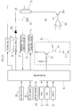
- Fig. 24 shows an embodiment in which flashing is stopped by using a voltage comparator instead of controlling the stop of flashing by checking the integrated light amount with the microcomputer. Except the following, this embodiment is similar to the forgoing embodiment shown in Figs. 16 through 21. A similar constituting member is denoted by the same reference numeral, and description thereof is omitted.
- the flash discharge tube 28 is connected to the main capacitor 26 in parallel, and a IGBT 61 is connected between them.
- the IGBT 61 is turned on prior to flashing and is turned off at the time of stopping the flash.
- a trigger circuit 62 applies a trigger voltage to the flash discharge tube 28 when the synchronizing signal is inputted from the shutter device 36 via a microcomputer 63. Hence, the electric charge of the main capacitor 26 is discharged in the flash discharge tube 28 via the IGBT being turned on so that flashing is started. In this embodiment, the successive flash is performed.
- a reference-voltage generating circuit 64 is controlled by the microcomputer 62 at the time of flashing, and outputs any one of reference voltages V N , V L and V D as a reference voltage V REF4 in accordance with the exposure correction mode selected by the setting button 14.
- the integral voltage V Cph from the light receiving circuit 50 is inputted into an inversion input terminal of a voltage comparator 65.
- the reference voltage V REF4 from the reference-voltage generating circuit 64 is inputted into a non-inversion terminal of the voltage comparator 65.
- the voltage comparator 65 sets a comparison signal to a "H level" when the integral voltage V Cph is less than the reference voltage V REF4 .
- the comparison signal is set to a "L level”.
- the "H level” of the comparison signal is adapted to be more than a gate voltage required for turning on the IGBT 61.
- the "L level” is set to 0 V, for example. Owing to this, the IGBT 61 is turned on when the integral voltage V Cph is less than the reference voltage V REF4 , and is turned off when the integral voltage V Cph reaches the reference voltage V REF4 .
- the IGBT 61 is turned on prior to flashing.
- the IGBT 61 is turned on by applying the reference voltage V REF4 (> 0 V) to the voltage comparator 65 when the integral voltage V Cph from the light receiving circuit 50 is substantially 0 V.
- V REF4 the reference voltage
- the phototransistor 18 receives the flash light reflected by a subject during flashing and the integral voltage V Cph reaches the reference voltage V REF4 , the IGBT 61 is turned off. Hence, connection between the flash discharge tube 28 and the main capacitor 26 is cut so that flashing is stopped.
- the microcomputer 63 controls the booster circuit 25, the trigger circuit 62, and the reference-voltage generating circuit 64. Besides these, the microcomputer 63 controls the sensitivity adjusting transistor 51 in accordance with the switching signal based on the ratio Ra so that the photosensitivity the light receiving circuit 50 is adjusted.
- the successive flash is started in synchronism with the operation of the shutter blade similarly to the conventional one. Then, a part of the flash light reflected by a subject is received by the phototransistor 18 during the successive flash. While the transistor 51 is turned on, the photocurrent corresponding to the received light amount flows to be charged in the capacitor 35. Thus, the integral voltage V Cph is raised. When the integral voltage V Cph reaches the reference voltage V REF4 , the comparison signal from the voltage comparator 65 is set to the "L level". Owing to this, the IGBT 61 is turned off so that flashing of one exposure is finished.
- the photosensitivity of the light receiving circuit 50 is adjusted in accordance with the ratio Ra.
- the flash-light amount relative to the instant photo film is regulated so as to correspond to the exposure correction mode selected by the setting button 14.
- the ratio Ra is determined, the set ratio Ra can be calculated from the exposure value EV T obtained by performing the test flash, the exposure value EV N corresponding to the normal mode, and the test ratio Ra T , using the reference voltage actually outputted from the reference-voltage generating circuit 64, for example the reference voltage V N .
- the ratio Ra is determined, the set ratio Ra can be calculated from the exposure value EV T obtained by performing the test flash, the exposure value EV N corresponding to the normal mode, and the test ratio Ra T , using the reference voltage actually outputted from the reference-voltage generating circuit 64, for example the reference voltage V N .
- the ratios Ra used in the respective exposure correction modes may be calculated and may be selectively used in accordance with the exposure correction mode. In this case, even if dispersion exists in the mutual ratio of the reference voltages V N , V L and V D , it is possible to obtain the proper exposure amounts corresponding to the respective exposure correction mode.
- stopping the flash may be controlled by using the voltage comparator.
- an AND operation is carried out, with an AND circuit, relative to the flash signal for the stepping flash and the output of the voltage comparator, for example.
- the obtained result is supplied to the IGBT 31 shown in Fig. 16 for example.
- Fig. 25 shows an embodiment in which the photosensitivity of the light receiving circuit is adjusted by changing a voltage applied to the phototransistor of the light receiving circuit, instead of changing the ratio Ra of the on-period to the cycle T for turning on and off the sensitivity adjusting transistor.
- a light receiving circuit 66 is constituted of the phototransistor 18, the capacitor 35, and an electric volume 67 being as a voltage applying member for outputting a voltage corresponding to a voltage-control signal.
- the electric volume 67 is constituted of a D-A converter and so forth, as well-known.
- applied-voltage data D V being as the voltage-control signal is inputted from the microcomputer 52
- the inputted applied-voltage data D V is linearly converted to a voltage and is outputted.
- the outputted voltage is applied to the collector terminal of the phototransistor 18.
- a voltage-control-signal generating section 52f of the microcomputer 52 inputs the applied voltage data D V into the electric volume 67 during flashing.
- the applied-voltage data D V is determined relative to each instant camera at the time of manufacturing and is written in the EEPROM 23.
- the other structure is similar to that shown in Fig. 17, and an identical member is denoted by the same reference numeral.
- the photocurrent flows in accordance with the light amount having entered the phototransistor 18, and this photocurrent is proportionally changed in response to the voltage applied from the electric volume 67 to the phototransistor 18.
- the photosensitivity of the light receiving circuit 66 may be adjusted.
- the applied-voltage data D V is determined, flashing is performed in a state that a proper voltage is applied from the electric volume 67 to the phototransistor 18, using any applied-voltage data D VT for testing. Then, flashing is stopped by the automatic light regulating function, using the reference voltage data D N for the normal mode, for example. The exposure value EV T obtained by this flash is measured by the adjusting device. The electric volume 67 linearly converts the applied-voltage data to the voltage. By utilizing this, it is possible to calculate the actually-used applied-voltage data D V with the following formula 6 ⁇ .
- the electric volume is used as the voltage applying member.
- the photosensitivity may be adjusted by changing the applied-voltage of the phototransistor, using another circuit or element.
- the voltage applying member is preferable to linearly convert the inputted voltage-control signal to the voltage.
- the photosensitivity is adjusted by changing its base current and by changing the applied voltage of the phototransistor.
- the base current may be determined by an operation similar to the forgoing formula 6 ⁇ within a working range of the transistor where the voltage between the emitter and the collector is linearly changed based on the base current. Meanwhile, within the working range where the voltage between the emitter and the collector is non-linearly changed, the base current needs to be determined on the basis of changing properties of the voltage between the emitter and the collector.
- the light-regulation level of the flash light may be adjusted by changing the applied-voltage data Dv in accordance with the exposure correction mode under a condition that the reference voltage V REF4 is fixed.
- the method for adjusting the photosensitivity by changing the applied voltage of the phototransistor is applicable to a case using the voltage comparator shown in Fig. 24. Moreover, this method is also applicable to a case in that the photocurrent from the phototransistor is converted to the light-reception voltage, and based on which the light amount is integrated.
- the present invention is applied to the flashing device incorporated in the instant camera.
- the flashing device according to the present invention is applicable to a camera using a photo film of the 135-type and so forth.
- the present invention is applicable to a flashing device incorporated in various cameras, for example a digital still camera.
- the present invention is applicable to a flashing device attached to a camera.
Landscapes
- Physics & Mathematics (AREA)
- General Physics & Mathematics (AREA)
- Stroboscope Apparatuses (AREA)
- Discharge-Lamp Control Circuits And Pulse- Feed Circuits (AREA)
- Exposure Control For Cameras (AREA)
Priority Applications (1)
| Application Number | Priority Date | Filing Date | Title |
|---|---|---|---|
| EP06008759A EP1698932A3 (de) | 1999-11-19 | 2000-11-15 | Blitzgerät mit automatischer Lichteinstellung |
Applications Claiming Priority (6)
| Application Number | Priority Date | Filing Date | Title |
|---|---|---|---|
| JP33031599 | 1999-11-19 | ||
| JP33031499 | 1999-11-19 | ||
| JP33031599 | 1999-11-19 | ||
| JP33031499 | 1999-11-19 | ||
| JP2000077735 | 2000-03-21 | ||
| JP2000077735 | 2000-03-21 |
Related Child Applications (1)
| Application Number | Title | Priority Date | Filing Date |
|---|---|---|---|
| EP06008759A Division EP1698932A3 (de) | 1999-11-19 | 2000-11-15 | Blitzgerät mit automatischer Lichteinstellung |
Publications (3)
| Publication Number | Publication Date |
|---|---|
| EP1102115A2 true EP1102115A2 (de) | 2001-05-23 |
| EP1102115A3 EP1102115A3 (de) | 2003-11-12 |
| EP1102115B1 EP1102115B1 (de) | 2007-08-29 |
Family
ID=27340408
Family Applications (2)
| Application Number | Title | Priority Date | Filing Date |
|---|---|---|---|
| EP00310117A Expired - Lifetime EP1102115B1 (de) | 1999-11-19 | 2000-11-15 | Blitzgerät mit automatischer Regelung der Lichtemission |
| EP06008759A Ceased EP1698932A3 (de) | 1999-11-19 | 2000-11-15 | Blitzgerät mit automatischer Lichteinstellung |
Family Applications After (1)
| Application Number | Title | Priority Date | Filing Date |
|---|---|---|---|
| EP06008759A Ceased EP1698932A3 (de) | 1999-11-19 | 2000-11-15 | Blitzgerät mit automatischer Lichteinstellung |
Country Status (7)
| Country | Link |
|---|---|
| US (1) | US6407512B1 (de) |
| EP (2) | EP1102115B1 (de) |
| JP (1) | JP2001337376A (de) |
| KR (1) | KR100647098B1 (de) |
| CN (1) | CN1251017C (de) |
| DE (1) | DE60036180T2 (de) |
| TW (1) | TW457394B (de) |
Cited By (1)
| Publication number | Priority date | Publication date | Assignee | Title |
|---|---|---|---|---|
| GB2547811B (en) * | 2016-04-15 | 2020-11-25 | Rotolight Ltd | Lighting device and control thereof |
Families Citing this family (15)
| Publication number | Priority date | Publication date | Assignee | Title |
|---|---|---|---|---|
| US6696799B2 (en) * | 2002-04-25 | 2004-02-24 | Star Headlight And Lantern Co., Inc. | Diagnostic system for a strobe lamp and its operating circuit |
| JP5051965B2 (ja) * | 2003-12-05 | 2012-10-17 | 株式会社ニコン | 撮影用照明装置、カメラシステムおよびカメラ |
| JP4565619B2 (ja) * | 2004-06-15 | 2010-10-20 | キヤノン株式会社 | カメラ |
| JP4724478B2 (ja) * | 2005-06-21 | 2011-07-13 | 株式会社リコー | 撮像装置、撮像制御方法およびコンピュータ読取り可能の記録媒体 |
| JP2007107926A (ja) | 2005-10-11 | 2007-04-26 | Rohm Co Ltd | 電流検出回路およびそれを用いた受光装置ならびに電子機器 |
| CN201182022Y (zh) * | 2007-08-24 | 2009-01-14 | 金毅 | 一种摄影灯装置 |
| JP2010244977A (ja) * | 2009-04-09 | 2010-10-28 | Renesas Electronics Corp | 半導体装置 |
| US8692887B2 (en) * | 2010-08-27 | 2014-04-08 | General Electric Company | Thermal imaging method and apparatus for evaluating coatings |
| GB201018572D0 (en) * | 2010-11-04 | 2010-12-15 | Reckitt & Colman Overseas | Refill recognition system and circuit |
| US9385158B2 (en) * | 2013-08-07 | 2016-07-05 | Pixart Imaging Inc. | Bipolar junction transistor pixel circuit, driving method thereof, and image sensor |
| JP6815826B2 (ja) | 2016-10-25 | 2021-01-20 | キヤノン株式会社 | 撮像装置、撮像システム及び自動照射方向制御方法 |
| JP7258589B2 (ja) | 2019-02-18 | 2023-04-17 | キヤノン株式会社 | 照明装置およびその制御方法、撮像装置 |
| CN110044480B (zh) * | 2019-04-03 | 2020-06-26 | 中国科学院西安光学精密机械研究所 | 闪烁光源控制电路、闪烁光源和线阵探测器同步控制电路及方法 |
| CN111836419B (zh) * | 2019-04-22 | 2022-11-04 | 浙江宇视科技有限公司 | 一种hid灯的控制方法及相关设备 |
| US12389126B2 (en) * | 2022-11-14 | 2025-08-12 | Sony Group Corporation | Lighting control for multi-view image capture |
Family Cites Families (14)
| Publication number | Priority date | Publication date | Assignee | Title |
|---|---|---|---|---|
| JPS5223932A (en) * | 1975-08-19 | 1977-02-23 | West Electric Co Ltd | Electronic flash device for photography |
| JPS56132317A (en) * | 1980-03-19 | 1981-10-16 | Minolta Camera Co Ltd | Photographing apparatus using auxiliary light |
| JPS5844428A (ja) * | 1981-09-11 | 1983-03-15 | Minolta Camera Co Ltd | 電子閃光装置 |
| JPH077844B2 (ja) * | 1981-11-30 | 1995-01-30 | 財団法人半導体研究振興会 | 静電誘導型半導体光電変換装置 |
| DD207269A1 (de) * | 1982-03-29 | 1984-02-22 | Pentacon Dresden Veb | Belichtungsmess- und -steuerschaltung |
| JPH0658485B2 (ja) * | 1985-03-11 | 1994-08-03 | 株式会社ニコン | 自動調光装置の増幅率切換回路 |
| US4785295A (en) * | 1986-02-27 | 1988-11-15 | Oki Electric Industry Co., Ltd. | Optical media monitoring device |
| JPS6417033A (en) * | 1987-07-10 | 1989-01-20 | Minolta Camera Kk | Automatic dimming system flash device |
| JP2801240B2 (ja) * | 1989-01-23 | 1998-09-21 | キヤノン株式会社 | 閃光装置 |
| US5248879A (en) * | 1992-10-19 | 1993-09-28 | Ncr Corporation | Circuit for adjusting the sensitivity of a sensor using a digital counter and a low-pass filter |
| JP3259447B2 (ja) * | 1993-06-29 | 2002-02-25 | 株式会社ニコン | 電子閃光制御システム |
| US5640623A (en) * | 1994-07-29 | 1997-06-17 | Olympus Optical Co., Ltd. | Wireless flash photographing system in which light emission control of a slave flash apparatus, situated away from a camera, is effected by a light signal from a master flash apparatus provided on the camera side |
| JPH09115682A (ja) * | 1995-10-20 | 1997-05-02 | Stanley Electric Co Ltd | 自動調光機能付ストロボ装置 |
| JP3689491B2 (ja) * | 1996-06-11 | 2005-08-31 | キヤノン株式会社 | ストロボ装置及びカメラ |
-
2000
- 2000-11-14 US US09/710,874 patent/US6407512B1/en not_active Expired - Lifetime
- 2000-11-15 EP EP00310117A patent/EP1102115B1/de not_active Expired - Lifetime
- 2000-11-15 EP EP06008759A patent/EP1698932A3/de not_active Ceased
- 2000-11-15 DE DE60036180T patent/DE60036180T2/de not_active Expired - Lifetime
- 2000-11-15 JP JP2000347861A patent/JP2001337376A/ja active Pending
- 2000-11-18 KR KR1020000068742A patent/KR100647098B1/ko not_active Expired - Lifetime
- 2000-11-18 TW TW089124475A patent/TW457394B/zh not_active IP Right Cessation
- 2000-11-19 CN CNB001370189A patent/CN1251017C/zh not_active Expired - Lifetime
Cited By (1)
| Publication number | Priority date | Publication date | Assignee | Title |
|---|---|---|---|---|
| GB2547811B (en) * | 2016-04-15 | 2020-11-25 | Rotolight Ltd | Lighting device and control thereof |
Also Published As
| Publication number | Publication date |
|---|---|
| EP1698932A3 (de) | 2007-01-31 |
| JP2001337376A (ja) | 2001-12-07 |
| KR20010051805A (ko) | 2001-06-25 |
| HK1035935A1 (en) | 2001-12-14 |
| EP1102115A3 (de) | 2003-11-12 |
| EP1102115B1 (de) | 2007-08-29 |
| CN1251017C (zh) | 2006-04-12 |
| DE60036180T2 (de) | 2007-12-20 |
| CN1314611A (zh) | 2001-09-26 |
| KR100647098B1 (ko) | 2006-11-17 |
| US6407512B1 (en) | 2002-06-18 |
| DE60036180D1 (de) | 2007-10-11 |
| TW457394B (en) | 2001-10-01 |
| EP1698932A2 (de) | 2006-09-06 |
Similar Documents
| Publication | Publication Date | Title |
|---|---|---|
| US6407512B1 (en) | Flashing device of an automatic light-regulation type | |
| US6349175B1 (en) | Flash photography system | |
| US6718135B2 (en) | Flash photography system | |
| US6826364B2 (en) | Zoom flash and flash photography system | |
| US5729772A (en) | Flashlight control apparatus | |
| US6512891B2 (en) | Electric flash device and camera | |
| US6571061B2 (en) | Uniform flash-emission controller | |
| HK1035935B (en) | Flash device with automatic light emission regulation | |
| JPH0961913A (ja) | カメラシステム | |
| JP3050655B2 (ja) | 赤目軽減機能付カメラ | |
| JP3658054B2 (ja) | 閃光撮影装置 | |
| JPS6364767B2 (de) | ||
| US6313907B1 (en) | Distance measurement system | |
| JPH1039368A (ja) | ストロボ制御カメラシステム | |
| JPH09146151A (ja) | ストロボ調光装置 | |
| JP3122446B2 (ja) | ストロボ制御装置 | |
| JPH05260369A (ja) | ストロボ発光制御装置 | |
| JP2001154246A (ja) | ストロボ装置 | |
| JP2001117147A (ja) | ストロボ装置及びその電圧データ決定方法 | |
| JP3703183B2 (ja) | ストロボ装置 | |
| JP2830369B2 (ja) | マルチ発光可能なフラッシュ装置 | |
| JPS63318531A (ja) | 電動ズ−ムカメラ | |
| JPH0915490A (ja) | 自動焦点調節装置及びカメラ | |
| JP2001117145A (ja) | ストロボ装置 | |
| JPH0954358A (ja) | ストロボシステム |
Legal Events
| Date | Code | Title | Description |
|---|---|---|---|
| PUAI | Public reference made under article 153(3) epc to a published international application that has entered the european phase |
Free format text: ORIGINAL CODE: 0009012 |
|
| AK | Designated contracting states |
Kind code of ref document: A2 Designated state(s): AT BE CH CY DE DK ES FI FR GB GR IE IT LI LU MC NL PT SE TR |
|
| AX | Request for extension of the european patent |
Free format text: AL;LT;LV;MK;RO;SI |
|
| RIC1 | Information provided on ipc code assigned before grant |
Ipc: 7H 05B 41/00 B Ipc: 7G 03B 15/05 B Ipc: 7G 03B 7/16 A |
|
| PUAL | Search report despatched |
Free format text: ORIGINAL CODE: 0009013 |
|
| AK | Designated contracting states |
Kind code of ref document: A3 Designated state(s): AT BE CH CY DE DK ES FI FR GB GR IE IT LI LU MC NL PT SE TR |
|
| AX | Request for extension of the european patent |
Extension state: AL LT LV MK RO SI |
|
| 17P | Request for examination filed |
Effective date: 20040421 |
|
| AKX | Designation fees paid |
Designated state(s): DE FR GB |
|
| 17Q | First examination report despatched |
Effective date: 20040817 |
|
| GRAP | Despatch of communication of intention to grant a patent |
Free format text: ORIGINAL CODE: EPIDOSNIGR1 |
|
| RAP1 | Party data changed (applicant data changed or rights of an application transferred) |
Owner name: FUJIFILM CORPORATION |
|
| GRAS | Grant fee paid |
Free format text: ORIGINAL CODE: EPIDOSNIGR3 |
|
| GRAA | (expected) grant |
Free format text: ORIGINAL CODE: 0009210 |
|
| AK | Designated contracting states |
Kind code of ref document: B1 Designated state(s): DE FR GB |
|
| REG | Reference to a national code |
Ref country code: GB Ref legal event code: FG4D |
|
| REF | Corresponds to: |
Ref document number: 60036180 Country of ref document: DE Date of ref document: 20071011 Kind code of ref document: P |
|
| ET | Fr: translation filed | ||
| REG | Reference to a national code |
Ref country code: HK Ref legal event code: WD Ref document number: 1035935 Country of ref document: HK |
|
| PLBE | No opposition filed within time limit |
Free format text: ORIGINAL CODE: 0009261 |
|
| STAA | Information on the status of an ep patent application or granted ep patent |
Free format text: STATUS: NO OPPOSITION FILED WITHIN TIME LIMIT |
|
| REG | Reference to a national code |
Ref country code: HK Ref legal event code: GR Ref document number: 1035935 Country of ref document: HK |
|
| 26N | No opposition filed |
Effective date: 20080530 |
|
| REG | Reference to a national code |
Ref country code: FR Ref legal event code: PLFP Year of fee payment: 16 |
|
| REG | Reference to a national code |
Ref country code: FR Ref legal event code: PLFP Year of fee payment: 17 |
|
| REG | Reference to a national code |
Ref country code: FR Ref legal event code: PLFP Year of fee payment: 18 |
|
| REG | Reference to a national code |
Ref country code: FR Ref legal event code: PLFP Year of fee payment: 19 |
|
| PGFP | Annual fee paid to national office [announced via postgrant information from national office to epo] |
Ref country code: DE Payment date: 20191105 Year of fee payment: 20 |
|
| PGFP | Annual fee paid to national office [announced via postgrant information from national office to epo] |
Ref country code: FR Payment date: 20191015 Year of fee payment: 20 |
|
| PGFP | Annual fee paid to national office [announced via postgrant information from national office to epo] |
Ref country code: GB Payment date: 20191115 Year of fee payment: 20 |
|
| REG | Reference to a national code |
Ref country code: DE Ref legal event code: R071 Ref document number: 60036180 Country of ref document: DE |
|
| REG | Reference to a national code |
Ref country code: GB Ref legal event code: PE20 Expiry date: 20201114 |
|
| PG25 | Lapsed in a contracting state [announced via postgrant information from national office to epo] |
Ref country code: GB Free format text: LAPSE BECAUSE OF EXPIRATION OF PROTECTION Effective date: 20201114 |