EP1102329A2 - Dielektrisches Element - Google Patents
Dielektrisches Element Download PDFInfo
- Publication number
- EP1102329A2 EP1102329A2 EP00310089A EP00310089A EP1102329A2 EP 1102329 A2 EP1102329 A2 EP 1102329A2 EP 00310089 A EP00310089 A EP 00310089A EP 00310089 A EP00310089 A EP 00310089A EP 1102329 A2 EP1102329 A2 EP 1102329A2
- Authority
- EP
- European Patent Office
- Prior art keywords
- film
- oxide
- element according
- capacitor
- conductor film
- Prior art date
- Legal status (The legal status is an assumption and is not a legal conclusion. Google has not performed a legal analysis and makes no representation as to the accuracy of the status listed.)
- Withdrawn
Links
Images


Classifications
-
- H—ELECTRICITY
- H10—SEMICONDUCTOR DEVICES; ELECTRIC SOLID-STATE DEVICES NOT OTHERWISE PROVIDED FOR
- H10B—ELECTRONIC MEMORY DEVICES
- H10B12/00—Dynamic random access memory [DRAM] devices
-
- H—ELECTRICITY
- H10—SEMICONDUCTOR DEVICES; ELECTRIC SOLID-STATE DEVICES NOT OTHERWISE PROVIDED FOR
- H10D—INORGANIC ELECTRIC SEMICONDUCTOR DEVICES
- H10D1/00—Resistors, capacitors or inductors
- H10D1/60—Capacitors
- H10D1/68—Capacitors having no potential barriers
- H10D1/692—Electrodes
- H10D1/696—Electrodes comprising multiple layers, e.g. comprising a barrier layer and a metal layer
-
- H—ELECTRICITY
- H10—SEMICONDUCTOR DEVICES; ELECTRIC SOLID-STATE DEVICES NOT OTHERWISE PROVIDED FOR
- H10D—INORGANIC ELECTRIC SEMICONDUCTOR DEVICES
- H10D1/00—Resistors, capacitors or inductors
- H10D1/60—Capacitors
- H10D1/68—Capacitors having no potential barriers
- H10D1/682—Capacitors having no potential barriers having dielectrics comprising perovskite structures
Definitions
- the present invention relates to a dielectric element, and more specifically, it relates to a dielectric element such as a capacitor element employing an oxide-based dielectric film.
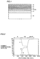
- FIGs. 29 and 30 are sectional views showing representative structures of conventional ferroelectric memories.
- an isolation oxide film 101, a well region 103 for a MOS transistor 102, a source region 104, a source electrode 105 connected with the source region 104, a gate electrode 106, a drain region 107 and an interlayer isolation film 114 are formed on an Si substrate 100.
- An oxide-based dielectric capacitor 113 is connected to the drain region 107 through a plug 109.
- an isolation oxide film 101, a well region 103 for a MOS transistor 102, a source region 104, a source electrode 105 connected with the source region 104, a gate electrode 106, a drain region 107, a drain electrode 108 connected with the drain region 107 and an interlayer isolation film 114 are formed on an Si substrate 100.
- An oxide-based dielectric capacitor 113 is connected to the gate electrode 106 through a plug 109.
- the structure shown in Fig. 30 is referred to as an FET-type ferroelectric memory.
- the oxide-based dielectric capacitor 113 is formed by a lower electrode 110, an oxide-based dielectric film 111 and an upper electrode 112.
- the lower electrode 110 is connected with the plug 109 made of polycrystalline silicon (poly-Si) or tungsten (W).
- the oxide-based dielectric film 111 of PbZr X Ti 1-X O 3 (PZT) or SrBi 2 Ta 2 O 9 (SBT) serving as a ferroelectric film is formed on the lower electrode 110.
- the upper electrode 112 is formed on the oxide-based dielectric film 111.
- iridium (Ir), platinum (Pt) or a material containing such a component is widely employed as the material for the lower electrode 110.
- the upper electrode 112 is also made of a material such as iridium (Ir) or platinum (Pt), similarly to the lower electrode 110. In each of the structures shown in Figs. 29 and 30, the upper electrode 112 is formed by an Ir film.
- DRAM dynamic random access memory
- the capacitor size is recently reduced following refinement of cells and hence a capacitor structure employing an oxide-based dielectric film of Ba X sr 1-X Tio 3 (BST) or the like having a high dielectric constant is required.
- BST Ba X sr 1-X Tio 3
- the capacitor structure of this DRAM is similar to that shown in Fig. 29.
- a silicon oxide film is formed between the lower electrode 110 and the plug 109.
- the silicon oxide film serves as a capacitor insulator film and is serially connected to the oxide-based dielectric capacitor 113.
- a bias applied thereto is divided in inverse proportion to the capacitance of each capacitor.
- the dielectric constant of an oxide-based dielectric film is generally several 10 to several 100 times that of a silicon oxide film, and hence the capacitance of the oxide-based dielectric capacitor 113 is increased.
- a bias applied in the state serially connecting the oxide-based dielectric capacitor 113 with the silicon oxide capacitor is not much divided to the oxide-based dielectric capacitor 113.
- a ferroelectric memory having the oxide-based dielectric film 111 of a ferroelectric film for example, its inverted polarization value is reduced to disadvantageously deteriorate the memory characteristics.
- a DRAM having the oxide-based dielectric film 111 of a high dielectric film its charging quantity is reduced to disadvantageously deteriorate the memory characteristics.
- the plug 109 When made of W in place of the aforementioned poly-Si in the element structure shown in Fig. 29, the plug 109 is partially oxidized to form a tungsten oxide film. In this case, film separation results from volume expansion caused by forming the tungsten oxide film, leading to such a problem that it is difficult to prepare a high-quality capacitor element.
- oxygen diffuses outward from the oxide-based dielectric film 111 along the grain boundaries of Ir or Pt forming the lower electrode 110 or the upper electrode 112, to disadvantageously deteriorate the characteristics such as the polarization characteristic of the oxide-based dielectric film 111 itself.
- Figs. 31 and 32 are schematic sectional views for illustrating problems of the prior art.
- a gigantic hillock (projection) 112a is readily formed on the surface of the upper electrode 112, as shown in Fig. 31 or 32.
- a plate line 116a is disadvantageously disconnected as shown in Fig. 31.
- an upper wire 118 formed on a plate wire 116b through an interlayer isolation film 117 is disadvantageously short-circuited to the plate wire 116b, as shown in Fig. 32.
- the Ir film forming the upper electrode 112 When oxidized, the Ir film forming the upper electrode 112 causes compositional change to inconveniently result in stress change of the Ir film. Therefore, the ferroelectric characteristics also disadvantageously tend to change.
- An object of the present invention is to provide a dielectric element having excellent characteristics by suppressing oxidation of an electrode.
- Another object of the present invention is to suppress deterioration of the characteristics of an oxide-based dielectric film in the aforementioned dielectric element.
- Still another object of the present invention is to provide a dielectric element capable of inhibiting the surface of an upper electrode from formation of a hillock (projection) by suppressing oxidation of the upper electrode.
- a further object of the present invention is to suppress stress change resulting from compositional change of an upper electrode material.
- a dielectric element comprises an insulator film including an oxide-based dielectric film and an electrode including a first conductor film containing at least a metal and silicon.
- the aforementioned metal includes at least one metal selected from a group consisting of Ir, Pt, Ru, Re, Ni, Co and Mo.
- the dielectric element is a wide concept including not only a capacitor element but also another element employing a dielectric material.
- the first conductor film serves as a barrier film for stopping diffusion of oxygen due to the aforementioned structure.
- oxygen can be effectively inhibited from diffusing along grain boundaries of the electrode in heat treatment for sintering the oxide-based dielectric film. Therefore, a conductive material located under the electrode can be inhibited from oxidation.
- deterioration of memory characteristics can be suppressed and film separation can be prevented in the case of a capacitor element, for example. Consequently, an element having excellent characteristics can be formed.
- the first conductor film preferably further contains nitrogen.
- the metal (M) forming the dielectric element according to the aforementioned aspect hardly forms a nitride in general, or is stabilized in a state of MxN (x ⁇ 2) when forming a nitride.
- the metal (M) is more readily bonded with Si than with N while N is readily bonded with Si. Therefore, the M-Si-N film conceivably has a structure obtained by embedding Si-N in metal silicide (M-Si).
- the M-Si-N film can conceivably have oxygen diffusion stoppability of the silicon nitride (Si-N) film and conductivity of the metal silicide (M-Si) at the same time. Consequently, the M-Si-N film can further improve the function of the first conductor film for stopping diffusion of oxygen.
- the metal forming the first conductor film is preferably iridium (Ir).
- the first conductor film can serve as the barrier film for stopping diffusion of oxygen.
- the first conductor film may be a conductor film containing iridium and silicon, or may be a conductor film containing iridium, silicon and nitrogen.
- the first conductor film may be formed by a multilayer structure of a conductor film containing iridium and silicon and a conductor film containing iridium, silicon and nitrogen.
- the conductor film containing iridium, silicon and nitrogen can keep high oxygen diffusion stoppability while the conductor film containing iridium and silicon can form a barrier film reduced in resistance.
- the conductor film containing iridium, silicon and nitrogen is preferably arranged on the side of the oxide-based dielectric film.
- the first conductor film can more effectively stop diffusion of oxygen from the oxide-based dielectric film. Therefore, deterioration of the characteristics of the oxide-based dielectric film itself can be suppressed.
- the first conductor film is preferably arranged between a conductive material and the insulator film.
- the first conductor film can effectively inhibit oxygen from diffusing into the conductive material from the insulating material.
- the conductive material is preferably converted to an insulating material when oxidized, and the first conductor film and the insulator film are preferably successively formed on the conductive material.
- the first conductor film can effectively inhibit oxygen from diffusing into the conductive material from the insulating material, thereby suppressing oxidation of the conductive material.
- the conductive material preferably includes either a polycrystalline silicon plug or a tungsten plug.
- the dielectric element according to the aforementioned aspect preferably further comprises a conductive crystal film arranged between the first conductor film and the insulator film.
- the first conductor film can stop diffusion of oxygen while the conductive crystal film can form an insulator film consisting of an oxide-based dielectric film having excellent characteristics such as a polarization characteristic.
- the conductive crystal film is preferably a metal film containing at least one metal selected from a group consisting of Pt, Ir, Ru and Re.
- the conductive crystal film consisting of the aforementioned metal film can form an insulator film consisting of an oxide-based dielectric film having excellent characteristics such as a polarization characteristic.
- the first conductor film preferably contains Pt, silicon and nitrogen, and the conductive crystal film is preferably a metal film consisting of Pt.
- the first conductor film containing Pt, silicon and nitrogen can more effectively stop diffusion of oxygen while the conductive crystal film consisting of the metal film of Pt can form an insulator film consisting of an oxide-based dielectric film having excellent characteristics such as a polarization characteristic.
- the conductive crystal film may be a metal oxide film containing at least one metal selected from a group consisting of Pt, Ir, Ru and Re.
- the conductive crystal film consisting of the aforementioned metal oxide film can form an insulator film consisting of an oxide-based dielectric film having excellent characteristics such as a polarization characteristic.
- the electrode including the first conductor film is preferably an upper electrode.
- the upper electrode can be effectively inhibited from oxidation.
- the surface of the upper electrode can be inhibited from formation of a hillock (projection) resulting from oxidation of the upper electrode. Consequently, disconnection of wires or short-circuiting across the wires can be suppressed.
- the material for the upper electrode can be inhibited from compositional change resulting from oxidation of the upper electrode.
- stress change of the upper electrode material can be suppressed, thereby suppressing change of the element characteristics.
- the first conductor film preferably further contains nitrogen.
- the function of the first conductor film for stopping diffusion of oxygen can be further improved.
- the first conductor film preferably contains Ir, silicon and nitrogen.
- the first conductor film preferably contains Ir, silicon and nitrogen. Therefore, high oxygen diffusion stoppability can be implemented by employing the first conductor film containing Ir, silicon and nitrogen. Therefore, the first conductor film (upper electrode) can be effectively inhibited from oxidation.
- the upper electrode preferably includes a plurality of layers, and at least the uppermost layer of the upper electrode is preferably formed by the first conductor film.
- the upper electrode is preferably formed by a multilayer structure of the first conductor film, containing Ir, silicon and nitrogen, forming the uppermost layer and a second conductor film containing Ir.
- a dielectric element comprises an insulator film including an oxide-based dielectric film and an upper electrode including a first conductor film containing TaN.
- the upper electrode can be effectively inhibited from oxidation when so formed as to include the first conductor film containing TaN having an excellent barrier property against diffusion of oxygen.
- the surface of the upper electrode can be inhibited from formation of a hillock (projection) resulting from oxidation of the upper electrode. Consequently, disconnection of wires and short-circuiting across the wires can be suppressed.
- compositional change of the upper electrode material resulting from oxidation of the upper electrode can be suppressed thereby suppressing stress change of the upper electrode material.
- Fig. 1 is a sectional view showing the structure of a capacitor element according to a first embodiment of the present invention.
- the capacitor element according to the first embodiment is formed through the following procedure: First, a doped poly-Si film 11 is formed on an Si substrate 10. An IrSi film 12 or an IrSiN film 13 is formed on the poly-Si film 11. Thereafter an Ir film 14 is formed on the IrSi film 12 or the IrSiN film 13. A ferroelectric SBT film 15 is formed on the Ir film 14 as an oxide-based dielectric film. Then, an Ir film 16 is formed on the SBT film 15. Then, annealing is performed in an oxygen atmosphere for sintering the SBT film 15.
- the poly-Si film 11 is 600 nm, the IrSi film 12 or the IrSiN film 13 is 100 nm, the Ir film 14 is 100 nm, the SBT film 15 is 300 nm and the Ir film 16 is 100 nm in thickness respectively.
- the Ir film 16 forms an upper electrode.
- the IrSi film 12 or the IrSiN film 13 and the Ir film 14 form a lower electrode.
- the poly-Si film 11 is an electrode material employed as part of the lower electrode or a plug.
- oxygen diffusion stoppability of the lower electrode formed by the IrSi film 12 or the IrSiN film 13 and the Ir film 14 has been investigated.
- Figs. 2 and 3 show results of element compositional ratios obtained by X-ray photoelectron spectroscopy (XPS) evaluation along the depth direction in a sample having a multilayer structure of Ir film 14/IrSi film 12/poly-Si film 11 similar to that shown in Fig. 1.
- Fig. 2 shows results obtained after forming the Ir/IrSi/poly-Si multilayer film
- Fig. 3 shows results obtained after annealing the sample in an oxygen atmosphere at 800°C for 40 minutes after forming the Ir/IrSi/poly-Si multilayer film. It is understood from the results shown in Fig.
- Figs. 4 and 5 show results of element compositional ratios obtained by XPS evaluation along the depth direction in another sample having a multilayer structure of Ir film 14/IrSiN film 13/poly-Si film 11 similar to that shown in Fig. 1.
- Fig. 4 shows results obtained after forming the Ir/IrSiN/poly-Si multilayer film
- Fig. 5 shows results obtained after annealing the sample in an oxygen atmosphere at 800°C for 40 minutes after forming the Ir/IrSiN/poly-Si multilayer film. It is understood from the results shown in Fig. 5 that oxygen diffusing by oxygen annealing is slightly stored on the interface between the Ir film 14 and the IrSiN film 13. It is also understood that the oxygen content is reduced in the IrSiN film 13. Thus, it is understood that the IrSiN film 13 stops diffusion of oxygen.
- the quantity of oxygen on the latter is smaller than that of the former.
- the IrSiN film 13 prepared by adding N to the IrSi film 12 has a higher function of stopping diffusion of oxygen than the IrSi film 12.
- the poly-Si film 11 was hardly oxidized on the interface between the poly-Si film 11 and the IrSi film 12 or the IrSiN film 13 in each of the samples having the multilayer structures of the Ir film 14/IrSi film 12/poly-Si film 11 and the Ir film 14/IrSiN film 13/poly-Si film 11.
- the IrSi film 12 or the IrSiN film 13 When a high-temperature oxygen annealing step is carried out on the structure obtained by successively forming the IrSi film 12 or the IrSiN film 13 and an oxide-based dielectric film such as the SBT film 15 on a conductive material such as the poly-Si film 11 converted to an insulating material when oxidized as in the first embodiment, the IrSi film 12 or the IrSiN film 13 serves as a barrier film for stopping diffusion of oxygen.
- the conductive material such as the poly-Si film 11 can be inhibited from oxidation.
- the IrSi film 12 has lower resistance than the IrSiN film 13 and hence a barrier film having low resistance and high oxygen diffusion stoppability can be formed with a multilayer film employing the IrSi film 12/IrSiN film 13.
- the poly-Si film 11 may be replaced with a W film or the Ir films 14 and 16 may be replaced with Pt films or metal films containing Ir or Pt in general.
- Fig. 6 is a sectional view showing the structure of a capacitor element according to a first example of the second embodiment of the present invention
- Fig. 7 is a sectional view showing the structure of a comparative capacitor element to be compared with the capacitor element according to the second embodiment of the present invention
- Fig. 8 is a sectional view showing the structure of a capacitor element according to a second example of the second embodiment of the present invention.
- the capacitor structure according to the first example of the second embodiment shown in Fig. 6 is formed through the following procedure: First, a WSi film 21 is formed on an Si substrate 20. Then, an interlayer isolation film 22 is formed. A contact hole 23 is formed through the interlayer isolation film 22. A doped poly-Si plug 24 is formed in the contact hole 23. An IrSiN film 25 connected with the poly-Si plug 24 is formed, followed by formation of an Ir film 26. A ferroelectric SBT film 27 is formed on the Ir film 26 as an oxide-based dielectric film. An Ir film 29 is formed on the SBT film 27. Annealing is performed in an oxygen atmosphere at 800°C for 40 minutes for sintering the SBT film 27.
- the IrSiN film 25, the Ir film 26, the SBT film 27 and the Ir film 29 are patterned by etching, thereby forming a capacitor 30.
- a hole 31 is formed for bringing a probe into contact with the WSi film 21.
- the comparative capacitor element structure shown in Fig. 7 is prepared by eliminating the IrSiN film 25 from the capacitor element structure according to the first example of the second embodiment shown in Fig. 6.
- the capacitor element structure according to the second example of the second embodiment shown in Fig. 8 is prepared by inserting an IrSiN film 28 between the SBT film 27 and the Ir film 29 in the capacitor element structure according to the first example of the second embodiment shown in Fig. 6.
- Fig. 6 shows the case of applying the IrSiN film 25 for stopping diffusion of oxygen to a lower electrode of the capacitor 30, and
- Fig. 8 shows the case of applying the IrSiN films 25 and 28 to lower and upper electrodes of the capacitor 30 respectively.
- the comparative capacitor element shown in Fig. 7 has no IrSiN films 25 and 28 applied to electrodes of the capacitor 30.
- the WSi film 21 is 500 nm and the poly-Si plug 24 is 800 nm in thickness respectively.
- the SBT film 27 employed as an oxide-based dielectric film is 300 nm in thickness.
- the IrSiN film 25 and the Ir film 26 forming the lower electrode in each of the capacitor elements according to the second embodiment shown in Figs. 6 and 8 are 100 nm and 200 nm in thickness respectively, while the Ir film 26 forming the lower electrode in the comparative capacitor element shown in Fig. 7 is 200 nm in thickness.
- the Ir film 29 forming the upper electrode in each of the capacitor elements shown in Figs. 6 and 7 is 300 nm in thickness
- the IrSiN film 28 and the Ir film 29 forming the upper electrode in the capacitor element shown in Fig. 8 are 100 nm and 200 nm in thickness respectively.
- Fig. 9 shows polarization hysteresis characteristics of the ferroelectric capacitors shown in Figs. 6 to 8 respectively.
- the vertical axis shows polarization values of ferroelectric substances
- the horizontal axis shows the strength of electric fields applied to the capacitors.
- Fig. 6 exhibits a loop (a) in Fig. 9.
- the hysteresis characteristic exhibits an excellent saturation characteristic and a value 2Pr (Pr: remanent polarization value) of about 9 ⁇ C/cm 2 .
- the comparative capacitor element shown in Fig. 7 exhibits a loop (b) in Fig. 9.
- the hysteresis characteristic exhibits no saturation characteristic and the value 2Pr thereof remains at about 2 ⁇ C/cm 2 .
- the IrSiN film 25 stopping diffusion of oxygen is inserted between the poly-Si plug 24 and the Ir film 26 thereby inhibiting oxygen from diffusing into the poly-Si plug 24, whereby an excellent hysteresis characteristic is obtained.
- the capacitor element shown in Fig. 8 exhibits a loop (c) in Fig. 9 and has a value 2Pr of about 11 ⁇ C/cm 2 higher than that of the capacitor element shown in Fig. 6.
- the reason for this is conceivably as follows: In the capacitor element structure shown in Fig. 6, oxygen diffuses from the SBT film 27 into the Ir film 29 in the annealing performed in the oxygen atmosphere to slightly deteriorate the film characteristics of the SBT film 27. In the capacitor element structure shown in Fig. 8, on the other hand, the IrSiN film 28 inserted between the SBT film 27 and the Ir film 29 stops diffusion of oxygen from the SBT film 27. Deterioration of the film characteristics of the SBT film 27 is conceivably therefore suppressed.
- an oxide-based dielectric film such as the SBT film 27 from deterioration of film characteristics resulting from annealing by inserting the IrSiN film 28 according to the present invention between a conductive material such as the Ir film 29 and the oxide-based dielectric film such as the SBT film 27.
- the inventive oxide-based dielectric capacitor element employing the IrSiN film 25 or 28 serving as a barrier film for stopping diffusion of oxygen can suppress oxidation of a conductive material such as the poly-Si plug 24 converted to an insulating material when oxidized or deterioration of film characteristics of an oxide-based dielectric film such as the SBT film 27 in a capacitor forming step. Consequently, excellent capacitor characteristics can be obtained.
- the barrier film is not restricted to this but an IrSi film or an IrSi/IrSiN multilayer film allowing reduction of resistance may alternatively be employed.
- the IrSiN film has higher oxygen diffusion stoppability and hence it is possible to effectively stop diffusion of oxygen from the oxide-based dielectric film by arranging the IrSiN film on the side of the SBT film employed as an oxide-based dielectric film.
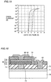
- FIG. 10 is a sectional view showing an exemplary structure of a ferroelectric memory according to a first example of the third embodiment of the present invention
- Fig. 11 is a sectional view showing the structure of a comparative ferroelectric memory to be compared with the ferroelectric memory according to the third embodiment of the present invention
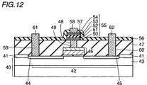
- Fig. 12 is a sectional view showing an exemplary structure of a ferroelectric memory according to a second example of the third embodiment of the present invention.
- the ferroelectric memory according to the first example of the third embodiment shown in Fig. 10 is formed through the following procedure: First, an isolation oxide film 41 and a well region 43 for a MOS transistor 42, a source region 44, a drain region 45 and a WSi/poly-Si gate electrode 46 are formed on a silicon substrate 40. Thereafter a first interlayer isolation film 47 is formed. A contact hole 48 is formed on the gate electrode 46, followed by formation of a poly-Si plug 49. Thereafter an IrSiN film 50 and an Ir film 51 are formed on the first interlayer isolation film 47 and the poly-Si plug 49. Then, a ferroelectric SBT film 52 is formed on the Ir film 51 as an oxide-based dielectric film.
- An Ir film 54 is formed on the SBT film 52. Annealing is performed in an oxygen atmosphere at 800°C for 40 minutes for sintering the SBT film 52. Thereafter the IrSiN film 50, the Ir film 51, the SBT film 52 and the Ir film 54 are patterned by etching, thereby forming a capacitor 55. After forming a second interlayer isolation film 56, a contact hole 57 is formed on the Ir film 54 forming an upper electrode of the capacitor 55. A conductive layer 58 is formed to fill up the contact hole 57.
- contact holes 59 and 60 are formed on the source region 44 and the drain region 45 respectively.
- a source electrode 61 and a drain electrode 62 are formed to fill up the contact holes 59 and 60 respectively.
- the conductive layer 58, the source electrode 61 and the drain electrode 62 are made of TiN/Al-Si-Cu/TiN/Ti or the like, for example.
- the interface between the Ir film 51 and the SBT film 52 is negatively charged and the interface between the gate electrode 46 and a gate insulator film is positively charged. Consequently, an inversion layer is formed on a channel region between the source region 44 and the drain region 45.
- the FET enters an ON state although the voltage of the conductive layer 58 and that of the Ir film 54 forming the upper electrode are zero.
- the interface between the Ir film 51 forming the lower electrode and the SBT film 52 is positively charged thereby negatively charging the interface between the gate electrode 46 and the gate insulator film. Consequently, no inversion layer is formed on the channel region between the source region 44 and the drain region 45 but the FET enters an OFF state.
- the FET can be selectively turned on or off also after setting the voltage applied to the conductive layer 58 as well as the Ir film 54 forming the upper electrode to zero.
- data "1" and "0" stored in the ferroelectric memory can be determined by detecting a source-to-drain current.
- the comparative ferroelectric memory structure shown in Fig. 11 is obtained by eliminating the IrSiN film 50 from the ferroelectric memory structure according to the first example of the third embodiment shown in Fig. 10.
- the ferroelectric memory structure according to the second example of the third embodiment shown in Fig. 12 is obtained by inserting an IrSiN film 53 between the SBT film 52 and the Ir film 54 in the ferroelectric memory structure according to the first example of the third embodiment shown in Fig. 10.
- the FET-type ferroelectric memory structure shown in Fig. 10 employs the IrSiN film 50 for stopping diffusion of oxygen as the lower electrode of the capacitor 55
- the FET-type ferroelectric memory structure shown in Fig. 12 employs the IrSiN films 50 and 53 as lower and upper electrodes of the capacitor 55 respectively.
- the comparative FET-type ferroelectric memory structure shown in Fig. 11 employs no IrSiN films 50 and 53 as electrodes of the capacitor 55.
- the capacitor element structures according to the third embodiment are similar to the three types of structures according to the aforementioned second embodiment.
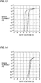
- Figs. 13 to 15 are graphs plotting drain currents and voltages (referred to as gate voltages) applied to the conductive layers 58 on the vertical and horizontal axes respectively.
- source and drain voltages are set to 0 V and 0.1 V respectively.
- the potential of the well region 43 is set identical to the source voltage.
- Fig. 13 shows the results of the ferroelectric memory according to the first example of the third embodiment shown in Fig. 10.
- the shift quantity of a threshold voltage Vt is about 2.0 V, as shown in Fig. 13.
- Fig. 14 shows the results of the comparative ferroelectric memory shown in Fig. 11. It is understood that the shift quantity of the threshold voltage Vt is only about 0.5 V in this case, as shown in Fig. 13.
- Fig. 14 shows the results of the ferroelectric memory according to the second example of the third embodiment shown in Fig. 12.
- the shift quantity of the threshold voltage Vt is further improved to 2.2 V as compared with the ferroelectric memory shown in Fig. 10, as shown in
- a ferroelectric memory having excellent storage characteristics can be prepared by applying the inventive oxide-based ferroelectric capacitor element employing the IrSiN film 50 or 53 serving as a barrier film for stopping diffusion of oxygen.
- Fig. 16 is a sectional view showing a capacitor element according to a fourth embodiment of the present invention.
- the capacitor structure according to the fourth embodiment shown in Fig. 16 is formed through the following procedure: First, an n-type doping layer 71 is formed on an Si substrate 70. An interlayer isolation film 72 is formed on the n-type doping layer 71. A contact hole 73 is formed through the interlayer isolation film 72. A poly-Si plug 74 is formed in the contact hole 73. A PtSiN barrier film 75 is formed to be connected with the poly-Si plug 74. Then, a Pt film 76 is formed on the PtSiN barrier film 75. A ferroelectric SBT film 77 is formed on the Pt film 76 as an oxide-based dielectric film.
- the SBT film 77 is formed by a sol-gel method. In this case, the SBT film 77 is prebaked under conditions of 300°C and five minutes. Thereafter a Pt film 78 is formed on the SBT film 77.
- the Pt film 78, the SBT film 77, the Pt film 76 and the PtSiN film 75 are patterned by etching, thereby forming a capacitor 90. Thereafter annealing is performed in an oxygen atmosphere at 800°C for 40 minutes, for sintering the SBT film 77.
- contact holes 80 and 81 are formed on the Pt film 78 and the n-type doping layer 71 respectively. Electrodes 82 and 83 are formed in the contact holes 80 and 81 respectively.
- the electrodes 82 and 83 are made of TiN/Al-Si-Cu/TiN/Ti or the like, for example.
- Fig. 17 is a sectional view showing the structure of a sample prepared for investigating oxygen diffusion stoppability of the PtSiN barrier film 75 according to the fourth embodiment.
- a multilayer structure of the PtSiN barrier film 75 and the poly-Si film 74 is formed on the Si substrate 70 in this sample.
- the prepared sample was annealed in an oxygen atmosphere at 800°C for 40 minutes, and thereafter an element compositional ratio was investigated by RBS (Rutherford backscattering spectrometry) along the depth of the multilayer structure.
- Fig. 18 shows the element compositional ratio of the multilayer film along the depth direction.
- the oxygen compositional ratio is reduced in the range of depth of about 20 nm from the surface in the PtSiN barrier film 75.
- the oxygen compositional ratio is not more than 5.2 %.
- the PtSiN barrier film 75 sufficiently stops diffusion of oxygen.
- the PtSiN film conceivably has a structure obtained by embedding Si-N in Pt-Si. It is conceivable that the PtSiN barrier film 75 consequently can have both the oxygen diffusion stoppability of a silicon nitride (Si-N) film and conductivity of Pt-Si (metal silicide).
- Fig. 19 is a sectional view showing a comparative capacitor structure prepared to be compared with the ferroelectric capacitor structure according to the fourth embodiment shown in Fig. 16.
- the comparative ferroelectric capacitor structure shown in Fig. 19 is prepared by eliminating the PtSiN barrier film 75 from the ferroelectric capacitor structure according to the fourth embodiment shown in Fig. 16.
- the thickness of the SBT film 77 is set to 200 nm.
- Fig. 20 shows results of polarization hysteresis characteristics of these capacitor structures.
- FIG. 20 the vertical and horizontal axes show polarization values of the ferroelectric substances and voltages applied to the capacitors respectively.
- a loop (a) in Fig. 20 shows the characteristics of the ferroelectric capacitor according to the fourth embodiment shown in Fig. 16, and a loop (b) in Fig. 20 shows the characteristics of the comparative ferroelectric capacitor shown in Fig. 19.
- the hysteresis characteristic of the capacitor structure according to the fourth embodiment shown in Fig. 16 exhibits an excellent saturation characteristic as shown in the loop (a) of Fig. 20, and the value 2Pr (Pr: remanent polarization value) thereof is about 13 ⁇ C/cm 2 .
- the hysteresis characteristic of the comparative capacitor structure shown in Fig. 19 exhibits no saturation characteristic and the value 2Pr thereof remains at about 2 ⁇ C/cm 2 , as shown in the loop (b) in Fig. 20.
- the PtSiN barrier film 75 for stopping diffusion of oxygen is inserted between the poly-Si plug 74 and the Pt film 76, thereby inhibiting oxygen from diffusing into the poly-Si plug 74. Therefore, the poly-Si plug 74 is not oxidized but an excellent hysteresis characteristic can be attained as a result.
- the inventive oxide-based dielectric capacitor element employing the PtSiN barrier film 75 serving as a barrier film for stopping diffusion of oxygen can suppress oxidation of a conductor film such as the poly-Si plug 74 converted to an insulating material when oxidized in a capacitor forming step. Consequently, an excellent capacitor characteristic can be attained.
- Fig. 21 is a sectional view showing a comparative capacitor structure prepared to be compared with the ferroelectric capacitor structure according to the fourth embodiment shown in Fig. 16.
- the comparative structure shown in Fig. 21 is obtained by eliminating the Pt film 76 from the ferroelectric capacitor according to the fourth embodiment shown in Fig. 16.
- Fig. 22 shows results of polarization hysteresis characteristics of these capacitor structures.
- the vertical and horizontal axes show polarization values of the ferroelectric substances and voltages applied to the capacitors respectively.
- a loop (a) in Fig. 22 shows the characteristics of the ferroelectric capacitor according to the fourth embodiment shown in Fig. 16, and a loop (b) in Fig. 22 shows the characteristics of the comparative ferroelectric capacitor shown in Fig. 21.
- the hysteresis characteristic of the capacitor structure according to the fourth embodiment shown in Fig. 16 exhibits an excellent saturation characteristic as shown in the loop (a) of Fig. 22, and the value 2Pr thereof is about 13 ⁇ C/cm 2 .
- the hysteresis characteristic of the comparative capacitor structure shown in Fig. 21 exhibits no saturation characteristic and the value 2Pr thereof remains at about 1 ⁇ C/cm 2 , as shown in the loop (b) in Fig. 22.
- the SBT film 77 When observing the comparative structure shown in Fig. 21 by SEM (scanning electron microscopy), the SBT film 77 exhibits a considerable quantity of space. Thus, this space serves as a capacitor serially connected to the capacitor 92 including the SBT film 77 similarly to the aforementioned capacitor formed by the SiO 2 film. It is conceivable that no sufficient voltage is therefore applied to the capacitor 92 including the SBT film 77. Such a large quantity of space is formed in the SBT film 77 conceivably because the initial growth nuclear concentration in crystallization of the SBT film 77 is small when forming the oxide-based dielectric film on amorphous PtSiN. In order to increase the initial growth nuclear concentration, it is preferable to form a crystal film such as the Pt film 76 and thereafter form the oxide-based dielectric film as in the fourth embodiment shown in Fig. 16.
- the quality of the SBT film 77 can be improved by inserting a conductive crystal film such as the Pt film 76 between the PtSiN barrier film 75 serving as a barrier film for stopping diffusion of oxygen and the SBT film 77 of an oxide dielectric material. Consequently, an excellent capacitor characteristic can be attained.
- Fig. 23 is a sectional view showing a ferroelectric capacitor element according to a fifth embodiment of the present invention.
- Fig. 24 is a sectional view showing a comparative ferroelectric capacitor element formed to be compared with the ferroelectric capacitor element according to the fifth embodiment shown in Fig. 23.
- the capacitor element according to the fifth embodiment of the present invention is formed through the following procedure: First, a tungsten silicide (WSi) film 2 is formed on an Si substrate 1. After forming an interlayer isolation film 3 on the WSi film 2, a contact hole 3a is formed through the interlayer isolation film 3. A polycrystalline silicon plug 4 consisting of doped polycrystalline silicon is formed in the contact hole 3a.
- WSi tungsten silicide
- An IrO 2 film 5 is formed to be connected with the polycrystalline silicon plug 4, and an Ir film 6 is formed thereon.
- the IrO 2 film 5 and the Ir film 6 form a capacitor lower electrode.
- An SBT film 7 serving as a ferroelectric film is formed on the Ir film 6.
- An IrSiN film 8 serving as a capacitor upper electrode is formed on the SBT film 7.
- the IrO 2 film 5, the Ir film 6, the SBT film 7 and the IrSiN film 8 are patterned by etching, thereby forming a capacitor 9. Thereafter annealing is performed for crystallizing the SBT film 7.
- the SBT film 7 corresponds to the "insulator film” of the present invention
- the IrSiN film 8 corresponds to the "first conductor film” and the "upper electrode” of the present invention.
- the fifth embodiment shown in Fig. 23 employs the IrSiN film 8 as the upper electrode of the ferroelectric capacitor 9.
- the comparative ferroelectric capacitor element shown in Fig. 24 employs an Ir film 208 in place of the IrSiN film 8 forming the upper electrode in the structure of the capacitor element according to the fifth embodiment shown in Fig. 23.
- the comparative ferroelectric capacitor element shown in Fig. 24 employs the Ir film 208 as an upper electrode of a ferroelectric capacitor 209.
- the remaining structure of the comparative capacitor shown in Fig. 24 is similar to that of the fifth embodiment shown in Fig. 23.
- annealing is performed in an oxygen atmosphere at 800°C for 40 minutes in crystallization of the SBT film 7 serving as a ferroelectric film.
- Fig. 25 is a microphotograph of the surface of the upper electrode subjected to oxygen annealing in the structure according to the fifth embodiment shown in Fig. 23 observed with an SEM
- Fig. 26 is a microphotograph of the surface of the upper electrode subjected to oxygen annealing in the comparative structure shown in Fig. 24 observed with an SEM.
- no hillock is formed when employing the IrSiN film 8 according to the fifth embodiment as the upper electrode, as shown in Fig. 25.
- hillocks (projections) having heights of about 1 ⁇ m at the maximum grow when employing the comparative Ir film 208 as the upper electrode, as shown in Fig. 26.
- Fig. 27 is a characteristic diagram showing results of element compositional ratios obtained by RBS with respect to an IrSiN (200 nm)/polycrystalline silicon (600 nm) film formed on a polycrystalline silicon film under the same conditions as the upper electrode according to the fifth embodiment shown in Fig. 23 after performing annealing in an oxygen atmosphere at 800°C for 40 minutes.
- Fig. 28 is a characteristic diagram showing results of element compositional ratios obtained by RBS with respect to an Ir (100 nm)/polycrystalline silicon (600 nm) film formed on a polycrystalline silicon film under the same conditions as the comparative upper electrode shown in Fig. 24 after performing annealing in an oxygen atmosphere at 800°C for 40 minutes.
- Table 1 shows values of film stress of the IrSiN film 8 employed in the fifth embodiment shown in Fig. 23 and the Ir film 208 employed in the comparative sample shown in Fig. 24 before and after oxygen annealing.
- Film Stress Before and After Annealing (unit:Pa) Before Annealing After Annealing IrSiN 4.94x10 8 4.29x10 8 Ir 3.8x10 9 6.1x10 7
Landscapes
- Semiconductor Memories (AREA)
Applications Claiming Priority (6)
| Application Number | Priority Date | Filing Date | Title |
|---|---|---|---|
| JP32654499 | 1999-11-17 | ||
| JP32654499 | 1999-11-17 | ||
| JP2000284892A JP2001210795A (ja) | 1999-11-17 | 2000-09-20 | 誘電体素子 |
| JP2000285667A JP3505497B2 (ja) | 1999-11-17 | 2000-09-20 | 誘電体素子 |
| JP2000285667 | 2000-09-20 | ||
| JP2000284892 | 2000-09-20 |
Publications (2)
| Publication Number | Publication Date |
|---|---|
| EP1102329A2 true EP1102329A2 (de) | 2001-05-23 |
| EP1102329A3 EP1102329A3 (de) | 2003-09-24 |
Family
ID=27340182
Family Applications (1)
| Application Number | Title | Priority Date | Filing Date |
|---|---|---|---|
| EP00310089A Withdrawn EP1102329A3 (de) | 1999-11-17 | 2000-11-14 | Dielektrisches Element |
Country Status (3)
| Country | Link |
|---|---|
| US (1) | US6720096B1 (de) |
| EP (1) | EP1102329A3 (de) |
| KR (1) | KR100744280B1 (de) |
Cited By (2)
| Publication number | Priority date | Publication date | Assignee | Title |
|---|---|---|---|---|
| US7057246B2 (en) | 2000-08-23 | 2006-06-06 | Reflectivity, Inc | Transition metal dielectric alloy materials for MEMS |
| US7071520B2 (en) | 2000-08-23 | 2006-07-04 | Reflectivity, Inc | MEMS with flexible portions made of novel materials |
Families Citing this family (4)
| Publication number | Priority date | Publication date | Assignee | Title |
|---|---|---|---|---|
| JP4753873B2 (ja) * | 2004-06-23 | 2011-08-24 | パトレネラ キャピタル リミテッド, エルエルシー | メモリ |
| JP4714590B2 (ja) * | 2006-01-23 | 2011-06-29 | パトレネラ キャピタル リミテッド, エルエルシー | メモリ |
| US8134275B2 (en) * | 2008-11-21 | 2012-03-13 | Trace Photonics, Inc. | High efficiency 4-π negatron β-3 particle emission source fabrication and its use as an electrode in a self-charged high-voltage capacitor |
| TWI698892B (zh) * | 2017-03-24 | 2020-07-11 | 日商村田製作所股份有限公司 | 電容器 |
Family Cites Families (41)
| Publication number | Priority date | Publication date | Assignee | Title |
|---|---|---|---|---|
| JPH02183569A (ja) | 1989-01-10 | 1990-07-18 | Seiko Epson Corp | 強誘電体記憶装置 |
| EP0415751B1 (de) * | 1989-08-30 | 1995-03-15 | Nec Corporation | Dünnfilmkondensator und dessen Herstellungsverfahren |
| DE69014027T2 (de) * | 1989-08-30 | 1995-06-01 | Nippon Electric Co | Dünnfilmkondensatoren und deren Herstellungsverfahren. |
| US5111355A (en) | 1990-09-13 | 1992-05-05 | National Semiconductor Corp. | High value tantalum oxide capacitor |
| US5504041A (en) | 1994-08-01 | 1996-04-02 | Texas Instruments Incorporated | Conductive exotic-nitride barrier layer for high-dielectric-constant materials |
| JP3683972B2 (ja) | 1995-03-22 | 2005-08-17 | 三菱電機株式会社 | 半導体装置 |
| US5822175A (en) | 1995-04-13 | 1998-10-13 | Matsushita Electronics Corporation | Encapsulated capacitor structure having a dielectric interlayer |
| US5883781A (en) * | 1995-04-19 | 1999-03-16 | Nec Corporation | Highly-integrated thin film capacitor with high dielectric constant layer |
| JP3417167B2 (ja) | 1995-09-29 | 2003-06-16 | ソニー株式会社 | 半導体メモリ素子のキャパシタ構造及びその形成方法 |
| US6004839A (en) | 1996-01-17 | 1999-12-21 | Nec Corporation | Semiconductor device with conductive plugs |
| JP3474352B2 (ja) | 1996-03-18 | 2003-12-08 | 株式会社東芝 | 薄膜キャパシタ及び半導体装置 |
| JPH09289291A (ja) | 1996-04-19 | 1997-11-04 | Texas Instr Japan Ltd | 誘電体キャパシタ及び誘電体メモリ装置と、これらの製造方法 |
| US5843830A (en) | 1996-06-26 | 1998-12-01 | Micron Technology, Inc. | Capacitor, and methods for forming a capacitor |
| JPH1093043A (ja) | 1996-09-13 | 1998-04-10 | Mitsubishi Electric Corp | キャパシタを有する半導体装置 |
| US6294420B1 (en) * | 1997-01-31 | 2001-09-25 | Texas Instruments Incorporated | Integrated circuit capacitor |
| JP3281839B2 (ja) | 1997-06-16 | 2002-05-13 | 三洋電機株式会社 | 誘電体メモリおよびその製造方法 |
| JPH1168057A (ja) | 1997-08-25 | 1999-03-09 | Sanyo Electric Co Ltd | 誘電体素子 |
| JP3212930B2 (ja) | 1997-11-26 | 2001-09-25 | 日本電気株式会社 | 容量及びその製造方法 |
| WO1999027579A1 (en) | 1997-11-26 | 1999-06-03 | Applied Materials, Inc. | Damage-free sculptured coating deposition |
| US6320213B1 (en) * | 1997-12-19 | 2001-11-20 | Advanced Technology Materials, Inc. | Diffusion barriers between noble metal electrodes and metallization layers, and integrated circuit and semiconductor devices comprising same |
| US6177351B1 (en) | 1997-12-24 | 2001-01-23 | Texas Instruments Incorporated | Method and structure for etching a thin film perovskite layer |
| KR100481982B1 (ko) * | 1997-12-30 | 2005-06-07 | 매그나칩 반도체 유한회사 | 트랜지스터의 게이트 전극 형성 방법 |
| US6178082B1 (en) | 1998-02-26 | 2001-01-23 | International Business Machines Corporation | High temperature, conductive thin film diffusion barrier for ceramic/metal systems |
| US5998258A (en) * | 1998-04-22 | 1999-12-07 | Motorola, Inc. | Method of forming a semiconductor device having a stacked capacitor structure |
| JP2000004001A (ja) | 1998-06-15 | 2000-01-07 | Toshiba Corp | 半導体記憶装置及びその製造方法 |
| JP2000040800A (ja) | 1998-07-24 | 2000-02-08 | Sharp Corp | 強誘電体記憶素子及びその製造方法 |
| JP3249481B2 (ja) | 1998-11-13 | 2002-01-21 | 株式会社東芝 | 半導体装置及びその製造方法 |
| KR100292692B1 (ko) | 1998-09-10 | 2001-07-12 | 김영환 | 반도체장치의커패시터제조방법 |
| JP3945043B2 (ja) | 1998-10-12 | 2007-07-18 | ソニー株式会社 | 金属窒化物膜の形成方法および電子装置の製造方法 |
| US6225656B1 (en) | 1998-12-01 | 2001-05-01 | Symetrix Corporation | Ferroelectric integrated circuit with protective layer incorporating oxygen and method for fabricating same |
| JP2000200886A (ja) | 1999-01-07 | 2000-07-18 | Hitachi Ltd | 半導体集積回路装置およびその製造方法 |
| JP4322347B2 (ja) | 1999-03-15 | 2009-08-26 | エルピーダメモリ株式会社 | 半導体装置およびその製造方法 |
| KR100316798B1 (ko) | 1999-03-16 | 2001-12-22 | 박종섭 | 반도체장치의 커패시터 및 그의 제조방법 |
| JP2000340769A (ja) | 1999-06-01 | 2000-12-08 | Mitsubishi Electric Corp | キャパシタの電極構造 |
| US6235603B1 (en) | 1999-07-12 | 2001-05-22 | Motorola Inc. | Method for forming a semiconductor device using an etch stop layer |
| US6916693B2 (en) | 2000-03-08 | 2005-07-12 | Semiconductor Energy Laboratory Co., Ltd. | Semiconductor device and manufacturing method thereof |
| JP2001257327A (ja) | 2000-03-10 | 2001-09-21 | Nec Corp | 半導体装置およびその製造方法 |
| JP2001274160A (ja) | 2000-03-24 | 2001-10-05 | Matsushita Electric Ind Co Ltd | 半導体装置およびその製造方法 |
| KR100396879B1 (ko) | 2000-08-11 | 2003-09-02 | 삼성전자주식회사 | 동일 물질로 이루어진 이중막을 포함하는 다중막으로캡슐화된 캐패시터를 구비한 반도체 메모리 소자 및 그의제조 방법 |
| US7057246B2 (en) | 2000-08-23 | 2006-06-06 | Reflectivity, Inc | Transition metal dielectric alloy materials for MEMS |
| JP2002134715A (ja) | 2000-10-23 | 2002-05-10 | Hitachi Ltd | 半導体集積回路装置およびその製造方法 |
-
2000
- 2000-11-14 US US09/711,512 patent/US6720096B1/en not_active Expired - Lifetime
- 2000-11-14 EP EP00310089A patent/EP1102329A3/de not_active Withdrawn
- 2000-11-16 KR KR1020000067936A patent/KR100744280B1/ko not_active Expired - Fee Related
Cited By (2)
| Publication number | Priority date | Publication date | Assignee | Title |
|---|---|---|---|---|
| US7057246B2 (en) | 2000-08-23 | 2006-06-06 | Reflectivity, Inc | Transition metal dielectric alloy materials for MEMS |
| US7071520B2 (en) | 2000-08-23 | 2006-07-04 | Reflectivity, Inc | MEMS with flexible portions made of novel materials |
Also Published As
| Publication number | Publication date |
|---|---|
| EP1102329A3 (de) | 2003-09-24 |
| KR100744280B1 (ko) | 2007-07-30 |
| US6720096B1 (en) | 2004-04-13 |
| KR20010051725A (ko) | 2001-06-25 |
Similar Documents
| Publication | Publication Date | Title |
|---|---|---|
| JP4428500B2 (ja) | 容量素子及びその製造方法 | |
| KR100281017B1 (ko) | 반도체 메모리 및 그 제조방법 | |
| US6046469A (en) | Semiconductor storage device having a capacitor and a MOS transistor | |
| JP3542704B2 (ja) | 半導体メモリ素子 | |
| US6180974B1 (en) | Semiconductor storage device having a capacitor electrode formed of at least a platinum-rhodium oxide | |
| CN100385668C (zh) | 多晶存储结构,形成该结构的方法,和使用该结构的半导体存储装置 | |
| US6624458B2 (en) | Semiconductor device having a ferroelectric capacitor and fabrication process thereof | |
| KR100504318B1 (ko) | 전자재료,그제조방법,유전체커패시터,불휘발성메모리및반도체장치 | |
| US6690054B2 (en) | Capacitor | |
| KR20060048987A (ko) | 강유전체 캐패시터, 그 제조 방법 및 강유전체 메모리 소자 | |
| US6888189B2 (en) | Dielectric element including oxide-based dielectric film and method of fabricating the same | |
| US5742472A (en) | Stacked capacitors for integrated circuit devices and related methods | |
| US6117689A (en) | Stable high-dielectric-constant material electrode and method | |
| US6727156B2 (en) | Semiconductor device including ferroelectric capacitor and method of manufacturing the same | |
| KR100590536B1 (ko) | 반도체 장치의 커패시터, 이를 포함하는 메모리 소자 및커패시터 제조 방법 | |
| US6720096B1 (en) | Dielectric element | |
| JP2001210795A (ja) | 誘電体素子 | |
| US6617626B2 (en) | Ferroelectric semiconductor memory device and a fabrication process thereof | |
| KR100442709B1 (ko) | 이종 질화물의 이중 방지막을 갖는 커패시터 및 그의 전극형성 방법 | |
| JPH08236719A (ja) | 白金薄膜、半導体装置及びそれらの製造方法 | |
| KR100576355B1 (ko) | 2단계 급속 열처리를 이용한 강유전체 메모리 소자의 제조방법 | |
| JP3505497B2 (ja) | 誘電体素子 | |
| JPH10150158A (ja) | 半導体メモリセルのキャパシタ構造の作製方法 | |
| JP2001267535A (ja) | 半導体装置 |
Legal Events
| Date | Code | Title | Description |
|---|---|---|---|
| PUAI | Public reference made under article 153(3) epc to a published international application that has entered the european phase |
Free format text: ORIGINAL CODE: 0009012 |
|
| AK | Designated contracting states |
Kind code of ref document: A2 Designated state(s): AT BE CH CY DE DK ES FI FR GB GR IE IT LI LU MC NL PT SE TR |
|
| AX | Request for extension of the european patent |
Free format text: AL;LT;LV;MK;RO;SI |
|
| PUAL | Search report despatched |
Free format text: ORIGINAL CODE: 0009013 |
|
| AK | Designated contracting states |
Kind code of ref document: A3 Designated state(s): AT BE CH CY DE DK ES FI FR GB GR IE IT LI LU MC NL PT SE TR |
|
| AX | Request for extension of the european patent |
Extension state: AL LT LV MK RO SI |
|
| AKX | Designation fees paid |
Designated state(s): DE FR GB NL |
|
| STAA | Information on the status of an ep patent application or granted ep patent |
Free format text: STATUS: THE APPLICATION IS DEEMED TO BE WITHDRAWN |
|
| 18D | Application deemed to be withdrawn |
Effective date: 20040325 |