EP1102527A2 - Boítier protégé contre les décharges électrostatiques - Google Patents
Boítier protégé contre les décharges électrostatiques Download PDFInfo
- Publication number
- EP1102527A2 EP1102527A2 EP00125186A EP00125186A EP1102527A2 EP 1102527 A2 EP1102527 A2 EP 1102527A2 EP 00125186 A EP00125186 A EP 00125186A EP 00125186 A EP00125186 A EP 00125186A EP 1102527 A2 EP1102527 A2 EP 1102527A2
- Authority
- EP
- European Patent Office
- Prior art keywords
- shielding housing
- shells
- circuit board
- housing
- housing according
- Prior art date
- Legal status (The legal status is an assumption and is not a legal conclusion. Google has not performed a legal analysis and makes no representation as to the accuracy of the status listed.)
- Granted
Links
- 229910052751 metal Inorganic materials 0.000 claims abstract description 18
- 239000002184 metal Substances 0.000 claims abstract description 18
- 229920003023 plastic Polymers 0.000 claims abstract description 9
- 239000004033 plastic Substances 0.000 claims abstract description 9
- 238000009423 ventilation Methods 0.000 claims description 13
- 230000000712 assembly Effects 0.000 claims description 6
- 238000000429 assembly Methods 0.000 claims description 6
- 238000001816 cooling Methods 0.000 claims description 5
- 210000002105 tongue Anatomy 0.000 claims description 5
- 238000004049 embossing Methods 0.000 claims description 3
- 230000008878 coupling Effects 0.000 claims description 2
- 238000010168 coupling process Methods 0.000 claims description 2
- 238000005859 coupling reaction Methods 0.000 claims description 2
- 230000006872 improvement Effects 0.000 claims description 2
- 230000002787 reinforcement Effects 0.000 claims description 2
- 239000003351 stiffener Substances 0.000 claims description 2
- 238000004519 manufacturing process Methods 0.000 description 9
- 230000008901 benefit Effects 0.000 description 5
- 230000006978 adaptation Effects 0.000 description 3
- 229910052782 aluminium Inorganic materials 0.000 description 3
- XAGFODPZIPBFFR-UHFFFAOYSA-N aluminium Chemical compound [Al] XAGFODPZIPBFFR-UHFFFAOYSA-N 0.000 description 3
- 238000010276 construction Methods 0.000 description 3
- 229910000831 Steel Inorganic materials 0.000 description 2
- 238000005452 bending Methods 0.000 description 2
- 238000005516 engineering process Methods 0.000 description 2
- 238000004080 punching Methods 0.000 description 2
- 239000010959 steel Substances 0.000 description 2
- RYGMFSIKBFXOCR-UHFFFAOYSA-N Copper Chemical compound [Cu] RYGMFSIKBFXOCR-UHFFFAOYSA-N 0.000 description 1
- 230000005540 biological transmission Effects 0.000 description 1
- 239000011248 coating agent Substances 0.000 description 1
- 238000000576 coating method Methods 0.000 description 1
- 239000004020 conductor Substances 0.000 description 1
- 229910052802 copper Inorganic materials 0.000 description 1
- 239000010949 copper Substances 0.000 description 1
- 238000009826 distribution Methods 0.000 description 1
- 230000000694 effects Effects 0.000 description 1
- 230000005672 electromagnetic field Effects 0.000 description 1
- 230000005670 electromagnetic radiation Effects 0.000 description 1
- 238000001125 extrusion Methods 0.000 description 1
- 230000017525 heat dissipation Effects 0.000 description 1
- 238000007373 indentation Methods 0.000 description 1
- 238000009434 installation Methods 0.000 description 1
- 238000009413 insulation Methods 0.000 description 1
- 238000005304 joining Methods 0.000 description 1
- 239000000463 material Substances 0.000 description 1
- 238000001465 metallisation Methods 0.000 description 1
- 238000012986 modification Methods 0.000 description 1
- 230000004048 modification Effects 0.000 description 1
- 238000007639 printing Methods 0.000 description 1
- 230000009467 reduction Effects 0.000 description 1
- 230000008439 repair process Effects 0.000 description 1
- 238000000926 separation method Methods 0.000 description 1
- 229910001220 stainless steel Inorganic materials 0.000 description 1
- 239000010935 stainless steel Substances 0.000 description 1
Images









Classifications
-
- H—ELECTRICITY
- H05—ELECTRIC TECHNIQUES NOT OTHERWISE PROVIDED FOR
- H05K—PRINTED CIRCUITS; CASINGS OR CONSTRUCTIONAL DETAILS OF ELECTRIC APPARATUS; MANUFACTURE OF ASSEMBLAGES OF ELECTRICAL COMPONENTS
- H05K9/00—Screening of apparatus or components against electric or magnetic fields
- H05K9/0062—Structures of standardised dimensions, e.g. 19" rack, chassis for servers or telecommunications
-
- H—ELECTRICITY
- H05—ELECTRIC TECHNIQUES NOT OTHERWISE PROVIDED FOR
- H05K—PRINTED CIRCUITS; CASINGS OR CONSTRUCTIONAL DETAILS OF ELECTRIC APPARATUS; MANUFACTURE OF ASSEMBLAGES OF ELECTRICAL COMPONENTS
- H05K7/00—Constructional details common to different types of electric apparatus
- H05K7/14—Mounting supporting structure in casing or on frame or rack
- H05K7/1461—Slidable card holders; Card stiffeners; Control or display means therefor
Definitions
- the invention relates primarily to a shield housing for receiving at least one component-equipped circuit board and / or assembly, which has metallic housing walls (preamble of claim 1).
- Printed circuit boards of the otherwise usual size in a closed It is known from DE 37 35 456 A1 to use a screen housing Guide means in the receiving device as webs and the guide means on Design the shield housing as grooves.
- the shield housing is made of sheet metal, the grooves being formed by impressions.
- the guide planes are formed from sheet metal cross members and a Carrying a plurality of webs which are punched out of the sheet metal surface and are bent sheet metal strips at right angles.
- cross beams can also be used be provided with only one web each, which as an elongated Sheet metal angles are formed, one leg of the sheet metal angle being the web.
- the front panel is attached to one on the front edge of the circuit board Angle plate attached and is higher than the shield housing itself, so that it both above and below on the outer dimensions of the screen housing protrudes. With these protruding sections of the front panel, it is on the Front of the frame's uprights held in T-shaped grooves Screwed threaded rails or sliding nuts.
- the disadvantage is however, that depends on the assembly of the circuit board or for each A corresponding setting must be made separately and that the assembly of mockery, crossbeam, shield housing and front panel a variety required by hand movements.
- the outer wall has two of the perforated shield plates, which are at least approximately at a distance extend parallel to each other.
- the outer wall can also be used as a separate wall part be formed, wherein at least one of the shield plates along the has circumferential edges of bent webs which are aligned with the other Overlap shield plate and the two shield plates in the overlap area are contacted.
- the two can essential flat shield plates z.
- a common connecting web can be connected in one piece, wherein the overlapping webs are formed along the remaining edges.
- On one side of the subrack facing away from the front is one Rear wall wiring plate arranged and the two shield plates have along the back, bent parallel to the backplane wiring board overlapping webs on which the backplane wiring board by means of screw-like fasteners is attached.
- the fasteners are passed through the two rear webs and brace the two webs with the backplane wiring board.
- DE 298 19 397 U1 is a shielding plate for a subrack -
- the to be equipped with electrical components and preferably for Installation in a distribution cabinet is intended - known, an upper one and / or a lower metallic shield for the purpose of shielding the Carried electrical components against electromagnetic fields are / is intended to with the metallic Side walls of the rack to be electrically connected.
- the shielding plate on its side walls edges adjacent to the subrack, preferably at right angles angled tabs is provided with mounting holes for attachment are provided on the side walls of the subrack.
- the Mounting holes are as threaded holes, as thread-free indentations or as threaded indents and the tabs are at or near the places where they emerge from the shielding plate with a Provide predetermined breaking point.
- the housing for receiving electronic Assemblies known, the construction of the electromagnetic radiation should reduce.
- the housing consists of two metallic U-shaped ones Housing walls (chassis and cover) and another housing part, which is to be inserted in the front cutout and the inclusion of, for example Drives.
- the two housing walls are overlapped by means of Fold and pre-locked grooves and tongues integrated therein during assembly then screwed, for example, as it is used by some common (Desktop) PC models are known ago.
- the use of overlapping folds with integrated grooves / springs serves to increase the EMC tightness At the same time, the aim is to make manufacturing and assembly easier.
- the chassis contains both the front and the back, while the cover contains the has both side walls.
- a stray radiation-proof housing is known from DE 43 09 084 A1, the housing for receiving a circuit board, made of two identical U-shaped Bowls and a front cover and which back with a backplane circuit board is completed. In detail here overlapping folds described.
- Shield housings often on one-piece housings or on housings resorted to, which is assembled from a variety of items or complete pre-assembled systems in one housing used, which are specially designed for the inclusion of these systems got to.
- the invention has for its object to provide a shield housing design that an inexpensive manufacture as well as a simple Assembly is made possible.
- This task is based on a shield housing with the features solved in the preamble of claim 1 in that the housing consists of two metallic half-shells, one side of one of the two Half shells is designed as a front panel, and that inside the housing at least one metal block or a metallized plastic block is attached, which is used for positive and / or non-positive fastening of the circuit board and an electrical connection between the two half shells and the Manufactures printed circuit board, whereby a central reference potential is available and the housing meets both EMC and ESD requirements.
- the housing is designed and exists in two-shell technology therefore essentially from only two housing parts, in which already the Front plate is integrated, which allows easy assembly of the housing makes. Since the two half shells are metallic (sheet steel, galvanized or nickel-plated or chrome-plated sheet steel or sheets of aluminum or Copper), they also serve as grounded shield plates, so that none additional shielding is necessary. Another advantage is that the Disposal effort is low and that an easy and cost effective Adaptation to different front parts and formats is possible. In particular is an adaptation to VME, VXI, CompactPCl and similar systems already feasible through minor modifications.
- the assembly or circuit board is already in one Half-shell can be firmly fixed with access to the assembly side (assembly side), what possible repair work and component replacement on the board considerably facilitated. Since the single half shell with the assembly also without the upper one Housing shell can be stably housed in the shield housing (bus housing) configuration of switches on the circuit board becomes significant facilitated.
- the two half-shells along the circumferential edges overlapping folds or the shell edges meet without overlap one on top of the other, with at least one of the two half-shells two outer walls with holes that are used for ventilation and cooling of the assembly.
- the front panel Recesses and / or slots in which elevations and / or tongues the other half shell are insertable.
- the two housing shells can be made in two different versions.
- the two shells have along the circumferential Edges overlapping edges, in the other version they butt without Overlap one another.
- the folds offer several advantages. For one let the two shells lock well together before screwing and get a higher stability. On the other hand, they increase the EMC tightness of the housing at the connection points.
- the ventilation holes in Honeycomb pattern with a maximum diameter of 4mm which means no additional EMC sheets or overlapping outer walls are necessary.
- the arrangement of the ventilation holes in the honeycomb pattern means that frequency range of interest an optimum between ventilation (narrow Bars) and EMC tightness achieved. If larger air holes than in claim 5 can be used, additional EMC sheets or overlapping outer walls of the two half-shells can be attached like this is described in claim 4 to the EMC tightness again to manufacture.
- Plastic holding parts according to claim 8 increase the positioning accuracy and can also be metallized as a whole (if there are no folds ), which further increases EMC tightness at connection points.
- the two half-shells cuts and this one in the middle Opening for fasteners, the circuit board on the counterbores lies on.
- the invention is based on a shield for interference sensitive and emitting electronic assemblies in Backplane bus systems described, the shield housing in Two-shell technology with an integrated front panel and which is on the Exterior of the housing (except for the countersinks 1, 2, 3 and 4) can be painted.
- the shielding housing according to the invention is for many applications suitable, for example in all digital transmission systems.
- the Drawing, especially FIG. 1 and FIG. 2 show a first embodiment of the shielding housing according to the invention in an exploded view or in perspective sectional view for receiving a component-equipped PCB and / or assembly, which has metallic housing walls having.
- the housing consists of two half-shells H1, H2, where the half-shell H1 is designed with an integrated front panel F.
- the PCB (assembly) is positive or non-positive in a half shell H1 attached in such a way that the shield housing has both EMC and ESD requirements justice.
- the two half shells H1, H2 can be along the have overlapping folds FZ or the shell edges collide without overlap (see comparison of FIG. 8 and FIG. 9).
- the shielding housing Fastening device for connecting the shielding housing to a Backplane bus system provided.
- the front panel F at least one recess BL is provided and the block arranged behind it M has at least one guide SF for at least one through the Shield housing operable fastener for fastening the Shielding housing in a backplane bus system.
- Below the recess BL can also have a recess embossed from the front, like this for example in FIG. 7 is shown.
- a galvanic coupling of the Module with front elements to be connected / external modules can done via the front panel F.
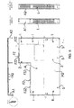
- the circuit board LP (An embodiment for the circuit board LP is shown in FIG.
- a assembly that can be inserted into the shielding housing from the rear carries at least one socket, for example a SUBD9 socket B1 *, one SUBD15 socket B2 * or an Ethernet socket B3 *, which is supported by the respective corresponding recess B1, B2 or B3 of the front panel F protrudes and attached to it.
- a SUBD9 socket B1 * for example a SUBD9 socket B1 *, one SUBD15 socket B2 * or an Ethernet socket B3 *, which is supported by the respective corresponding recess B1, B2 or B3 of the front panel F protrudes and attached to it.
- the RB * socket of the Backplane bus system Further recesses in the front panel F, such as for example the two slots SP and LED (see FIG. 7 or FIG. 8), are used to insert a PCMCIA memory card or an LED display or light guide from the front.
- At least two Outer walls A1, A2 of the shield housing have holes L leading to the Ventilation and cooling of the module serve (see for example FIG. 6).
- the Ventilation holes L can also have a honeycomb pattern with a diameter of maximum 4mm, which means for the frequency range of interest no additional EMC sheets are required.
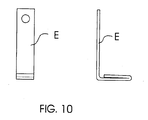
- a metal block or a metallized plastic block M is attached, for receiving and Fixing the circuit board and an electrical connection between the upper and lower shell Hl, H2 of the housing, the circuit board and an earth angle E manufactures, whereby a central reference potential is available.
- the blocks M are for example made of aluminum and as screw guides SF when fastening the shield housing in the backplane bus system executed and can preferably be used to guide the ground contact E (Earth angle).
- the two Half shells H1, H2 countersinks 1, 2, 3, 4, I, II (for example produced by emboss) with a central opening for fasteners have, and on the depressions 1, 2, 3, 4, I, II, the circuit board LP.
- one of the countersink 1, 2, 3, 4, I, II can spatially assigned, pot-like and a central bore supporting element are provided, in each of which a connecting means for fastening Immersed upper and lower shell Hl, H2 of the housing.
- you can Press-in threaded bushes are provided.
- the in FIG. 11 shown hatched rectangles (for I, II) are the areas for the EARTH connection and the hatched circles (at 1, 2, 3, 4) indicate restricted areas without components and with plated-through holes and conductor tracks on outer layers.
- the blocks M can also be used to fix the rear wall R (sheet metal rear wall) and / or to maintain the grid spacing (specified by the bus system Distance between the two housing shells).
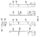
- the block M is preferably of an essentially L-shaped configuration and carries to maintain the grid spacing at least one vertically upright Elevation RA (see for example FIG. 4 and FIG. 5).
- the rear wall R is designed as an essentially elongated plate, which carries tongues RZ on the two long sides, the slots S of the two Insert half-shells H1, H2 (see FIG. 3).
- the central reference potential of the housing via contacts on the rear wall of the housing to the outside (e.g. via bolts for hanging from aluminum or Stainless steel).
- the inside of the Shield housing on the two rails of the backplane bus system Block M attached a facing groove or a groove Has projection for receiving and fixing the circuit board LP, wherein in this area of the circuit board LP is provided with a ground plane.
- the rear wall side of the shielding housing has the metallic angle E attached, creating an electrical connection between the two Half shells H1, H2, the circuit board LP and the earth angle E is produced and a central reference potential is available.
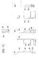
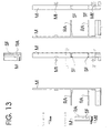
- FIG. 12 to 15 show a second embodiment of the invention Shielding housing for double height or grid spacing.
- Shielding housing for double height or grid spacing.
- Those lying on the ground surface of the PCB LP Overhangs of the block M are labeled MI and MII and have one Hole for the passage of fasteners or guides (see FIG. 12 and FIG. 13).
- Front plate F integrated in the L-shaped upper shell H2.
- the lower shell is H1 Designed in a U-shape and has the two outer walls A1, A2.
- A2 of the lower shell H1 are provided with bends FH, which engage in corresponding recesses FS of the upper shell H2 (see FIG. 14 and FIG. 15).
- the upper shell H2 has a depression TY for attaching a nameplate.
- Block M is still not a complex manufacturing process, especially with the metallization, as this is necessary for the entire Block M and can also be done without a mask.
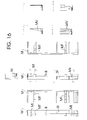
- the block contains M for the guidance of the assemblies, preferably guide rails MF (see FIG. 16 and FIG. 17). Stiffeners MV are also used to improve stability or stability and / or contact threaded bushings III provided.
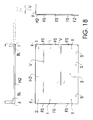
- the upper shell H2 and the lower shell H1 have reinforcements V in the form of embossments or ribs for stiffening (see FIG. 18 and FIG. 19).
- the upper shell H2 can be provided with a partial front panel F and the lower shell H1 has punched-out punchings A like this in FIG. 18 and FIG. 19 is shown.
- the blocks M can be a substantially closed Have shape in the region of the holes L; etc.
Landscapes
- Engineering & Computer Science (AREA)
- Microelectronics & Electronic Packaging (AREA)
- Shielding Devices Or Components To Electric Or Magnetic Fields (AREA)
- Mounting Of Printed Circuit Boards And The Like (AREA)
- Transmitters (AREA)
- Casings For Electric Apparatus (AREA)
Priority Applications (1)
| Application Number | Priority Date | Filing Date | Title |
|---|---|---|---|
| DE20022907U DE20022907U1 (de) | 2000-11-20 | 2000-11-20 | Abschirmgehäuse mit ESD-Schutz |
Applications Claiming Priority (2)
| Application Number | Priority Date | Filing Date | Title |
|---|---|---|---|
| DE19956184A DE19956184A1 (de) | 1999-11-22 | 1999-11-22 | Abschirmgehäuse |
| DE19956184 | 1999-11-22 |
Publications (3)
| Publication Number | Publication Date |
|---|---|
| EP1102527A2 true EP1102527A2 (fr) | 2001-05-23 |
| EP1102527A3 EP1102527A3 (fr) | 2002-01-23 |
| EP1102527B1 EP1102527B1 (fr) | 2007-03-21 |
Family
ID=7929951
Family Applications (1)
| Application Number | Title | Priority Date | Filing Date |
|---|---|---|---|
| EP00125186A Expired - Lifetime EP1102527B1 (fr) | 1999-11-22 | 2000-11-20 | Boîtier protégé contre les décharges électrostatiques |
Country Status (3)
| Country | Link |
|---|---|
| EP (1) | EP1102527B1 (fr) |
| AT (1) | ATE357842T1 (fr) |
| DE (2) | DE19956184A1 (fr) |
Families Citing this family (1)
| Publication number | Priority date | Publication date | Assignee | Title |
|---|---|---|---|---|
| DE10223170A1 (de) | 2002-05-24 | 2003-12-18 | Siemens Ag | EMV-Abschirmung für elektronische Bauelemente und EMV-Gehäuse |
Family Cites Families (7)
| Publication number | Priority date | Publication date | Assignee | Title |
|---|---|---|---|---|
| DE3313970A1 (de) * | 1983-04-18 | 1984-10-18 | Siemens AG, 1000 Berlin und 8000 München | Vorrichtung zum sicheren herstellen von elektrisch leitenden verbindungen zwischen gehaeuseteilen eines gehaeuses |
| DE8903217U1 (de) * | 1989-03-15 | 1990-07-12 | Philips Patentverwaltung Gmbh, 2000 Hamburg | Leiterplattengehäuse |
| DE4309084C2 (de) * | 1993-03-20 | 2003-02-27 | Philips Corp Intellectual Pty | Störstrahlsicheres Gehäuse |
| US5544008A (en) * | 1994-06-30 | 1996-08-06 | International Business Machines Corporation | Computer expansion module apparatus |
| GB2292483B (en) * | 1994-08-18 | 1998-12-23 | Sega Enterprises Kk | Shielding construction for shielding noise generated by an electronic circuit |
| US5808237A (en) * | 1995-11-13 | 1998-09-15 | Gateway 2000, Inc. | Electronics case for reducing electromagnetic radiation |
| JP2719905B2 (ja) * | 1995-11-17 | 1998-02-25 | 株式会社三共 | 弾球遊技機 |
-
1999
- 1999-11-22 DE DE19956184A patent/DE19956184A1/de not_active Withdrawn
-
2000
- 2000-11-20 EP EP00125186A patent/EP1102527B1/fr not_active Expired - Lifetime
- 2000-11-20 DE DE50014179T patent/DE50014179D1/de not_active Expired - Lifetime
- 2000-11-20 AT AT00125186T patent/ATE357842T1/de not_active IP Right Cessation
Also Published As
| Publication number | Publication date |
|---|---|
| ATE357842T1 (de) | 2007-04-15 |
| EP1102527B1 (fr) | 2007-03-21 |
| DE19956184A1 (de) | 2001-06-21 |
| EP1102527A3 (fr) | 2002-01-23 |
| DE50014179D1 (de) | 2007-05-03 |
Similar Documents
| Publication | Publication Date | Title |
|---|---|---|
| EP2683230B1 (fr) | Coffret | |
| EP0415246B1 (fr) | Rack électronique | |
| EP0014391A1 (fr) | Système d'unité enfichable et support pour circuits electronique | |
| EP1072179B1 (fr) | Support de modules | |
| EP0313131A2 (fr) | Dispositif de logement de cartes blindées | |
| DE3417451C2 (de) | Einschub-Gehäuse | |
| DE4114484C2 (de) | Baugruppenträger | |
| EP1102527B1 (fr) | Boîtier protégé contre les décharges électrostatiques | |
| EP0886999A1 (fr) | Dispositif de recouvrement de faible hauteur pour boitiers metalliques a blindage electromagnetique | |
| EP0516986B1 (fr) | Rack électronique | |
| DE19609887C1 (de) | Gerätechassis für elektronische Geräte | |
| EP0886992B1 (fr) | Chassis pour appareils electroniques | |
| DE20022907U1 (de) | Abschirmgehäuse mit ESD-Schutz | |
| EP0419949B1 (fr) | Tôle de blindage d'étage de rack électronique | |
| EP0653906B1 (fr) | Dispositif pour boîte électronique pour assemblages étendue de components électronique | |
| EP3270666B1 (fr) | Dispositif de logement d'unités de construction électroniques | |
| DE60223782T2 (de) | Kombination von Frontplatten | |
| EP0934591B1 (fr) | Ensemble d'elements pour systeme de montage | |
| EP4322716B1 (fr) | Boîtier pour circuit électrique et procédé de fabrication associé | |
| EP0886998B1 (fr) | Moulure profilee angulaire pour chassis equipee a protection electromagnetique | |
| DE3624756C2 (fr) | ||
| EP1623609B1 (fr) | Unite d'alimentation electrique | |
| DE10007493C2 (de) | Gehäuse zur Aufnahme elektrischer und/oder elektronische Einbauten | |
| EP1543707B1 (fr) | Chassis | |
| DE102024118228A1 (de) | Steuergerät mit einer eine Vielzahl von Durchschrauböffnungen aufweisenden und zwischen zwei Leiterplatten angeordneten Halteeinrichtung und Fahrzeug |
Legal Events
| Date | Code | Title | Description |
|---|---|---|---|
| PUAI | Public reference made under article 153(3) epc to a published international application that has entered the european phase |
Free format text: ORIGINAL CODE: 0009012 |
|
| AK | Designated contracting states |
Kind code of ref document: A2 Designated state(s): AT BE CH CY DE DK ES FI FR GB GR IE IT LI LU MC NL PT SE TR |
|
| AX | Request for extension of the european patent |
Free format text: AL;LT;LV;MK;RO;SI |
|
| PUAL | Search report despatched |
Free format text: ORIGINAL CODE: 0009013 |
|
| AK | Designated contracting states |
Kind code of ref document: A3 Designated state(s): AT BE CH CY DE DK ES FI FR GB GR IE IT LI LU MC NL PT SE TR |
|
| AX | Request for extension of the european patent |
Free format text: AL;LT;LV;MK;RO;SI |
|
| RIC1 | Information provided on ipc code assigned before grant |
Free format text: 7H 05K 9/00 A, 7H 05K 7/14 B |
|
| AKX | Designation fees paid | ||
| REG | Reference to a national code |
Ref country code: DE Ref legal event code: 8566 |
|
| 17P | Request for examination filed |
Effective date: 20020918 |
|
| RBV | Designated contracting states (corrected) |
Designated state(s): AT BE CH CY DE DK ES FI FR GB GR IE IT LI LU MC NL PT SE TR |
|
| 17Q | First examination report despatched |
Effective date: 20050308 |
|
| GRAP | Despatch of communication of intention to grant a patent |
Free format text: ORIGINAL CODE: EPIDOSNIGR1 |
|
| GRAS | Grant fee paid |
Free format text: ORIGINAL CODE: EPIDOSNIGR3 |
|
| GRAA | (expected) grant |
Free format text: ORIGINAL CODE: 0009210 |
|
| AK | Designated contracting states |
Kind code of ref document: B1 Designated state(s): AT BE CH CY DE DK ES FI FR GB GR IE IT LI LU MC NL PT SE TR |
|
| PG25 | Lapsed in a contracting state [announced via postgrant information from national office to epo] |
Ref country code: FI Free format text: LAPSE BECAUSE OF FAILURE TO SUBMIT A TRANSLATION OF THE DESCRIPTION OR TO PAY THE FEE WITHIN THE PRESCRIBED TIME-LIMIT Effective date: 20070321 Ref country code: NL Free format text: LAPSE BECAUSE OF FAILURE TO SUBMIT A TRANSLATION OF THE DESCRIPTION OR TO PAY THE FEE WITHIN THE PRESCRIBED TIME-LIMIT Effective date: 20070321 Ref country code: IE Free format text: LAPSE BECAUSE OF FAILURE TO SUBMIT A TRANSLATION OF THE DESCRIPTION OR TO PAY THE FEE WITHIN THE PRESCRIBED TIME-LIMIT Effective date: 20070321 |
|
| REG | Reference to a national code |
Ref country code: GB Ref legal event code: FG4D Free format text: NOT ENGLISH |
|
| REG | Reference to a national code |
Ref country code: CH Ref legal event code: EP |
|
| REF | Corresponds to: |
Ref document number: 50014179 Country of ref document: DE Date of ref document: 20070503 Kind code of ref document: P |
|
| REG | Reference to a national code |
Ref country code: IE Ref legal event code: FG4D Free format text: LANGUAGE OF EP DOCUMENT: GERMAN |
|
| PG25 | Lapsed in a contracting state [announced via postgrant information from national office to epo] |
Ref country code: SE Free format text: LAPSE BECAUSE OF FAILURE TO SUBMIT A TRANSLATION OF THE DESCRIPTION OR TO PAY THE FEE WITHIN THE PRESCRIBED TIME-LIMIT Effective date: 20070621 |
|
| PG25 | Lapsed in a contracting state [announced via postgrant information from national office to epo] |
Ref country code: ES Free format text: LAPSE BECAUSE OF FAILURE TO SUBMIT A TRANSLATION OF THE DESCRIPTION OR TO PAY THE FEE WITHIN THE PRESCRIBED TIME-LIMIT Effective date: 20070702 |
|
| PG25 | Lapsed in a contracting state [announced via postgrant information from national office to epo] |
Ref country code: PT Free format text: LAPSE BECAUSE OF FAILURE TO SUBMIT A TRANSLATION OF THE DESCRIPTION OR TO PAY THE FEE WITHIN THE PRESCRIBED TIME-LIMIT Effective date: 20070821 |
|
| NLV1 | Nl: lapsed or annulled due to failure to fulfill the requirements of art. 29p and 29m of the patents act | ||
| GBV | Gb: ep patent (uk) treated as always having been void in accordance with gb section 77(7)/1977 [no translation filed] |
Effective date: 20070321 |
|
| REG | Reference to a national code |
Ref country code: IE Ref legal event code: FD4D |
|
| EN | Fr: translation not filed | ||
| PG25 | Lapsed in a contracting state [announced via postgrant information from national office to epo] |
Ref country code: GB Free format text: LAPSE BECAUSE OF FAILURE TO SUBMIT A TRANSLATION OF THE DESCRIPTION OR TO PAY THE FEE WITHIN THE PRESCRIBED TIME-LIMIT Effective date: 20070321 |
|
| PLBE | No opposition filed within time limit |
Free format text: ORIGINAL CODE: 0009261 |
|
| STAA | Information on the status of an ep patent application or granted ep patent |
Free format text: STATUS: NO OPPOSITION FILED WITHIN TIME LIMIT |
|
| 26N | No opposition filed |
Effective date: 20071227 |
|
| PG25 | Lapsed in a contracting state [announced via postgrant information from national office to epo] |
Ref country code: FR Free format text: LAPSE BECAUSE OF FAILURE TO SUBMIT A TRANSLATION OF THE DESCRIPTION OR TO PAY THE FEE WITHIN THE PRESCRIBED TIME-LIMIT Effective date: 20071123 Ref country code: GR Free format text: LAPSE BECAUSE OF FAILURE TO SUBMIT A TRANSLATION OF THE DESCRIPTION OR TO PAY THE FEE WITHIN THE PRESCRIBED TIME-LIMIT Effective date: 20070622 Ref country code: IT Free format text: LAPSE BECAUSE OF FAILURE TO SUBMIT A TRANSLATION OF THE DESCRIPTION OR TO PAY THE FEE WITHIN THE PRESCRIBED TIME-LIMIT Effective date: 20070321 |
|
| BERE | Be: lapsed |
Owner name: IAD G.- FUR INFORMATIK, AUTOMATISIERUNG UND DATEN Effective date: 20071130 |
|
| PG25 | Lapsed in a contracting state [announced via postgrant information from national office to epo] |
Ref country code: MC Free format text: LAPSE BECAUSE OF NON-PAYMENT OF DUE FEES Effective date: 20071130 |
|
| PG25 | Lapsed in a contracting state [announced via postgrant information from national office to epo] |
Ref country code: LI Free format text: LAPSE BECAUSE OF NON-PAYMENT OF DUE FEES Effective date: 20071130 Ref country code: CH Free format text: LAPSE BECAUSE OF NON-PAYMENT OF DUE FEES Effective date: 20071130 |
|
| REG | Reference to a national code |
Ref country code: CH Ref legal event code: PL |
|
| PG25 | Lapsed in a contracting state [announced via postgrant information from national office to epo] |
Ref country code: BE Free format text: LAPSE BECAUSE OF NON-PAYMENT OF DUE FEES Effective date: 20071130 |
|
| PG25 | Lapsed in a contracting state [announced via postgrant information from national office to epo] |
Ref country code: FR Free format text: LAPSE BECAUSE OF FAILURE TO SUBMIT A TRANSLATION OF THE DESCRIPTION OR TO PAY THE FEE WITHIN THE PRESCRIBED TIME-LIMIT Effective date: 20070321 |
|
| PG25 | Lapsed in a contracting state [announced via postgrant information from national office to epo] |
Ref country code: AT Free format text: LAPSE BECAUSE OF NON-PAYMENT OF DUE FEES Effective date: 20071120 |
|
| PG25 | Lapsed in a contracting state [announced via postgrant information from national office to epo] |
Ref country code: CY Free format text: LAPSE BECAUSE OF FAILURE TO SUBMIT A TRANSLATION OF THE DESCRIPTION OR TO PAY THE FEE WITHIN THE PRESCRIBED TIME-LIMIT Effective date: 20070321 |
|
| PG25 | Lapsed in a contracting state [announced via postgrant information from national office to epo] |
Ref country code: LU Free format text: LAPSE BECAUSE OF NON-PAYMENT OF DUE FEES Effective date: 20071120 Ref country code: DK Free format text: LAPSE BECAUSE OF FAILURE TO SUBMIT A TRANSLATION OF THE DESCRIPTION OR TO PAY THE FEE WITHIN THE PRESCRIBED TIME-LIMIT Effective date: 20070621 |
|
| PG25 | Lapsed in a contracting state [announced via postgrant information from national office to epo] |
Ref country code: TR Free format text: LAPSE BECAUSE OF FAILURE TO SUBMIT A TRANSLATION OF THE DESCRIPTION OR TO PAY THE FEE WITHIN THE PRESCRIBED TIME-LIMIT Effective date: 20070321 |
|
| PGFP | Annual fee paid to national office [announced via postgrant information from national office to epo] |
Ref country code: DE Payment date: 20191115 Year of fee payment: 20 |
|
| REG | Reference to a national code |
Ref country code: DE Ref legal event code: R071 Ref document number: 50014179 Country of ref document: DE |