EP1107314A1 - Strahlenfester MOS-Transistor - Google Patents
Strahlenfester MOS-Transistor Download PDFInfo
- Publication number
- EP1107314A1 EP1107314A1 EP00410153A EP00410153A EP1107314A1 EP 1107314 A1 EP1107314 A1 EP 1107314A1 EP 00410153 A EP00410153 A EP 00410153A EP 00410153 A EP00410153 A EP 00410153A EP 1107314 A1 EP1107314 A1 EP 1107314A1
- Authority
- EP
- European Patent Office
- Prior art keywords
- type
- transistors
- transistor
- region
- drain
- Prior art date
- Legal status (The legal status is an assumption and is not a legal conclusion. Google has not performed a legal analysis and makes no representation as to the accuracy of the status listed.)
- Withdrawn
Links
- 230000005855 radiation Effects 0.000 title 1
- 239000000758 substrate Substances 0.000 claims abstract description 19
- 230000015654 memory Effects 0.000 claims description 16
- 239000002245 particle Substances 0.000 description 12
- 230000015572 biosynthetic process Effects 0.000 description 5
- 230000000295 complement effect Effects 0.000 description 5
- 238000005516 engineering process Methods 0.000 description 5
- 238000000034 method Methods 0.000 description 5
- 230000003071 parasitic effect Effects 0.000 description 5
- 230000010287 polarization Effects 0.000 description 5
- XUIMIQQOPSSXEZ-UHFFFAOYSA-N Silicon Chemical compound [Si] XUIMIQQOPSSXEZ-UHFFFAOYSA-N 0.000 description 4
- 238000004519 manufacturing process Methods 0.000 description 4
- 230000009467 reduction Effects 0.000 description 4
- 229910052710 silicon Inorganic materials 0.000 description 4
- 239000010703 silicon Substances 0.000 description 4
- 239000004065 semiconductor Substances 0.000 description 3
- 238000010586 diagram Methods 0.000 description 2
- 230000000694 effects Effects 0.000 description 2
- 238000012986 modification Methods 0.000 description 2
- 230000004048 modification Effects 0.000 description 2
- 230000008569 process Effects 0.000 description 2
- 230000002745 absorbent Effects 0.000 description 1
- 239000002250 absorbent Substances 0.000 description 1
- XAGFODPZIPBFFR-UHFFFAOYSA-N aluminium Chemical compound [Al] XAGFODPZIPBFFR-UHFFFAOYSA-N 0.000 description 1
- 229910052782 aluminium Inorganic materials 0.000 description 1
- 230000008859 change Effects 0.000 description 1
- 239000012212 insulator Substances 0.000 description 1
- 150000002500 ions Chemical class 0.000 description 1
- 239000000463 material Substances 0.000 description 1
- 229910021421 monocrystalline silicon Inorganic materials 0.000 description 1
- 244000045947 parasite Species 0.000 description 1
- 230000035945 sensitivity Effects 0.000 description 1
- 230000003068 static effect Effects 0.000 description 1
Images

Classifications
-
- H—ELECTRICITY
- H10—SEMICONDUCTOR DEVICES; ELECTRIC SOLID-STATE DEVICES NOT OTHERWISE PROVIDED FOR
- H10B—ELECTRONIC MEMORY DEVICES
- H10B10/00—Static random access memory [SRAM] devices
-
- H—ELECTRICITY
- H10—SEMICONDUCTOR DEVICES; ELECTRIC SOLID-STATE DEVICES NOT OTHERWISE PROVIDED FOR
- H10D—INORGANIC ELECTRIC SEMICONDUCTOR DEVICES
- H10D89/00—Aspects of integrated devices not covered by groups H10D84/00 - H10D88/00
- H10D89/60—Integrated devices comprising arrangements for electrical or thermal protection, e.g. protection circuits against electrostatic discharge [ESD]
- H10D89/601—Integrated devices comprising arrangements for electrical or thermal protection, e.g. protection circuits against electrostatic discharge [ESD] for devices having insulated gate electrodes, e.g. for IGFETs or IGBTs
- H10D89/611—Integrated devices comprising arrangements for electrical or thermal protection, e.g. protection circuits against electrostatic discharge [ESD] for devices having insulated gate electrodes, e.g. for IGFETs or IGBTs using diodes as protective elements
Definitions
- the present invention relates generally to insulated gate type transistors (MOS). More specifically, the present invention relates to protection - or hardening - such MOS transistors with respect to ionizing particles.
- MOS insulated gate type transistors
- a first approach is to plan around the device shielding, for example aluminum, absorbent particle energy.
- Such shielding is bulky and expensive, especially since it must be thick to be able to absorb most energetic particles.
- a second approach consists in modifying the circuit to allow a cell to return to its original state after a disturbance.
- Such modifications consist, by example, to provide additional cells (redundancy), or to modify the very structure of elementary SRAM cells to six transistors to guarantee the locking of memorized data.
- all of these changes reduce dramatically cell performance for example in terms of access time and / or overconsumption.
- a third approach is to modify the technology for manufacturing MOS transistors. So we used silicon on insulator (SOI) technologies. Although the reductions performance (access time, overconsumption, size) observed is then lower than with other techniques already proposed, such technologies are particularly complex and expensive to implement.
- SOI silicon on insulator
- An object of the present invention is to provide a new MOS transistor structure which exhibits hardening high to ionizing particles.
- Another object of the present invention is to provide such a structure which induces constraints (complexity, negligible manufacturing cost, or at least significantly lower than those induced by the solutions currently proposed.
- Another object of the present invention is to provide a hardened SRAM type memory cell structure using the transistors according to the invention.
- Another object of the present invention is to provide such a hardened memory structure which takes up space limited compared to existing solutions.
- Another object of the present invention is to provide such a hardened memory structure that exhibits performance comparable to those of a conventional memory.
- the present invention provides a lateral type MOS transistor comprising a gate and drain and source regions of a first type of conductivity formed in a substrate of a second type of conductivity connected to a first supply, comprising a buried layer doped with the first type of conductivity extending under said drain region and under part of the grid, the buried layer being connected to the grid via a link with unidirectional conduction.
- the unidirectional conduction means is a diode whose cathode is connected to the transistor gate and the anode to the buried layer.
- connection of the substrate to the first supply is ensured by a deeply doped deep region of the second type of conductivity extending to a more heavily doped portion of said substrate.
- the present invention also provides a cell SRAM type memory, including two first N-channel transistors of the cell have structures according to the embodiment previous, and including two second P-channel transistors of the cell are made in an N type box close to the area in which the first transistors are formed, the regions of drain of the second transistors being formed near said heavily doped region of the first transistors.
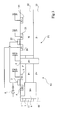
- FIG. 1 illustrates, in partial sectional view and schematic, an N channel MOS transistor N1 produced according to the principles of the present invention.
- the transistor N1 is formed in a surface area 1 of an epitaxial layer 11 itself formed on a slice of monocrystalline silicon 10.
- Zone 1, layer 11 and wafer 10 are all P-type doped, wafer 10 being the most heavily doped region and the weakest layer 11 doped.
- An isolated grid 2, formed above zone 1, defines a channel area.
- On either side of grid 2 is find strongly doped source 3 and drain 4 regions type N, formed in zone 1.
- a heavily doped region 5 type P serves as substrate contact.
- Contact region 5 and the source 3 are connected to the same GND reference potential, by example, the mass of the system.
- the structure also comprises a buried layer 6 heavily doped with type N.
- Layer 6 extends under the entire drain region 4 and under part of the channel. However, it does not reach the vertical of the region of source 3.
- Layer 6 and grid 2 are interconnected at by means of a unidirectional conduction link.
- the link comprises for example an N-type well 7 formed between layer 6 and the surface of zone 1 and a PN type diode 8 whose cathode is connected to grid 2 and the anode to well 7.
- the diode 8 can advantageously be carried out monolithically from anyway known.
- transistor N1 The operation of transistor N1 is as follows.
- transistor N1 In the case where the gate 2 and the drain 4 of the transistor N1 are polarized at the high Vdd supply, region 5 and the source 3 being always polarized at the GND reference potential, transistor N1 is on. Due to the presence of the diode 8, the buried layer 6 does not affect the operation of the transistor N1. In fact, layer 6 has the same ground potential GND, at a voltage drop near the junction, that the layer epitaxially surrounding 11. To improve this polarization at reference potential, for example, of zero value, we predict a deep conductive region 5 crossing region 1 and the epitaxial layer 11 and reaching the silicon wafer underlying 10 more heavily doped.
- layer 6 should be chosen so not to disturb the distribution of equipotentials under the grid and around the drain-substrate junction. However, it layer 6 must be close enough to drain 4 so that the charges created by the passage of an ionizing particle in the structure are absorbed.
- the doping of the layer 6 is high, especially so that layer 6 is conductive enough to quickly transfer loads parasites to ground.
- Additional elements (buried layer 6, well 7, diode 8) to be introduced into a conventional structure to obtain a structure according to the invention described above are advantageously simple and inexpensive to produce and not entraining practically no increase in surface area of the component.
- the present invention is particularly applicable the production of complementary transistors in the same substrate, for example to make type memory cells SRAM.
- Figure 2 is an electrical diagram of a memory cell SRAM type.
- This cell has four transistors, namely two transistors N1 and N2 with N channel and two transistors P1 and P2 with P channel.
- the transistors N1 and N2 are interconnected by their respective sources 3 and 13 at the same low power supply GND.
- the transistors P1 and P2 are interconnected by their respective sources 23 and 33 to the same high Vdd power supply.
- the transistors N1, N2, P1 and P2 are associated in two pairs N1-P1 and N2-P2 as follows. Drains 4-24, 14-34 and grids 2-22, 12-32 of the two transistors of a same pair N1-P1, N2-P2 are interconnected.
- the midpoint of drain interconnects 4-24, 14-34 of a pair N1-P1, N2-P2 is connected to the common point of grid 12-32, 2-22 of the other pair N2-P2, N1-P1.
- the N-channel transistors of this cell which are the most sensitive to ionizing particles can advantageously be made according to the invention.
- FIG. 3 illustrates an embodiment according to the present invention of two complementary transistors, corresponding to the transistors NI and P1 of FIG. 2 formed in a same semiconductor chip.
- the left part of figure 3 represents the transistor N1 of Figure 1 formed in a surface area 1 of a epitaxial layer 11 more weakly doped with type P than the underlying tranche 10. Zone 1 is more heavily doped than layer 11.
- the transistor N1 has, as before, a grid 2, source 3 and drain 4 regions, region 5 of substrate contact, a buried layer 6 and a bond to unidirectional conduction between layer 6 and grid 2. We assume as before that source 3 and region 5 are polarized to the GND reference potential of the circuit.
- the same section 10 also includes, to the right of the figure, a P-channel transistor P1.
- This is formed in a well 42 of type N.
- the transistor P1 comprises regions heavily doped P-type, respectively constituting its source 23 and its drain 24, formed on the surface of the box 42 on the one hand and on the other side of a channel zone defined by an isolated grid 22.
- a heavily doped N-type region 35 formed on the surface of the box 42 provides substrate contact for transistor P1. Source 23 and region 35 are polarized by the high Vdd power supply.
- Figure 3 illustrates the connection of the drain 4 and of gate 2 of transistor N1 respectively to drain 24 and to the gate 22 of the transistor P1, in accordance with the structure of the figure 2.
- Such connections are made using any usual process for forming such conductive bonds.
- the region polarization deep 5 will preferably be, as is shown, close in top view of the drain region 24.
- Figure 4 is a schematic perspective view of a embodiment of the SRAM cell of FIG. 2 in a semiconductor wafer 10 heavily doped type P, according to principles exposed in figure 3.
- the N1, N2 transistors with N channel are formed in an area 1 of an epitaxial layer 11 doped with P type.
- the P channel P1, P2 transistors are formed in a N 42 type box formed on the surface of wafer 10.
- the transistors of the same type are aligned so as to have a common source region. In top view, we therefore see a drain - grid - source - grid - drain sequence.
- a diaper buried heavily doped type N (not shown) is under each drain region 4, 14 of the transistors N1, N2.
- Each layer buried is connected to the gate 2, 12 of the transistor by via a well 7, 17 and a diode 8, 18.
- the cathode diode 8, 18 is connected to the grid 2, 12 while its anode is connected to well 7, 17.
- Regions are also formed of contact substrate 5 and 35 respectively in zone 1 and in the box 42.
- the region 35 is a surface region little deep as region 5 crosses zone 1 and layer 11 and reaches the heavily doped P-type wafer 10.
- Region 5 is preferably formed near the boundary between zone 1 and the box 42, to ensure the polarization of the wafer 10 at the reference potential below the drain regions 24-34 of transistors P1, P2, as explained previously in relationship to Figure 3.
- the memory cell described above ( Figure 2), produced according to the principles of the invention set out in relation to Figures 1 and 3, advantageously has a high hardening. It will indeed require ionizing particles with an energy transfer per unit of length (Linear Energy Transfer) of more than substantially 120 MeV.cm 2 / mg to cause untimely citations from the cell, which is beyond standards common curing.
- Linear Energy Transfer Linear Energy Transfer
- the additional space introduced by the formation of the two buried layers, of the two wells 7, 17 and of the two diodes 8, 18 is less than that of the solutions to redundancy or cell with at least ten transistors.
- the additional junctions formed introduce negligible parasitic capacities before those related to the formation of grid structures additional.
- a structure according to the invention is also advantageous. Indeed, as explained in connection with FIG. 2, in the absence disturbances, the operation of the transistors is not not modified and no additional resistance is introduced. In the presence of ionizing particles bombarding a region of drain of an N channel transistor, the overconsumption introduced by the resistance of layer 6 is negligible compared to that caused by the high resistances necessary for decoupling resistive.
- the present invention is capable of various variants and modifications which will appear to the man of art.
- those skilled in the art will understand that one could apply a such hardening process to the formation of other types of devices.
Landscapes
- Semiconductor Memories (AREA)
- Metal-Oxide And Bipolar Metal-Oxide Semiconductor Integrated Circuits (AREA)
Applications Claiming Priority (2)
| Application Number | Priority Date | Filing Date | Title |
|---|---|---|---|
| FR9915564A FR2802339B1 (fr) | 1999-12-09 | 1999-12-09 | Transistor mos durcis |
| FR9915564 | 1999-12-09 |
Publications (1)
| Publication Number | Publication Date |
|---|---|
| EP1107314A1 true EP1107314A1 (de) | 2001-06-13 |
Family
ID=9553081
Family Applications (1)
| Application Number | Title | Priority Date | Filing Date |
|---|---|---|---|
| EP00410153A Withdrawn EP1107314A1 (de) | 1999-12-09 | 2000-12-08 | Strahlenfester MOS-Transistor |
Country Status (3)
| Country | Link |
|---|---|
| US (1) | US6630719B2 (de) |
| EP (1) | EP1107314A1 (de) |
| FR (1) | FR2802339B1 (de) |
Families Citing this family (11)
| Publication number | Priority date | Publication date | Assignee | Title |
|---|---|---|---|---|
| US20030018970A1 (en) * | 2001-07-19 | 2003-01-23 | Digeo, Inc. | Object representation of television programs within an interactive television system |
| JP4016192B2 (ja) * | 2002-08-19 | 2007-12-05 | ソニー株式会社 | 固体撮像装置とその製造方法 |
| DE10254415A1 (de) * | 2002-11-21 | 2004-08-05 | Infineon Technologies Ag | Feldeffekttransistorstruktur, zugehörige Halbleiter-Speicherzelle sowie zugehöriges Herstellungsverfahren |
| US7250650B2 (en) * | 2002-11-21 | 2007-07-31 | Infineon Technologies Ag | Field-effect transistor structure and associated semiconductor memory cell |
| US20050040546A1 (en) * | 2003-05-12 | 2005-02-24 | Cuchiaro Joseph D. | Radiation hardened microelectronic device |
| WO2004102641A2 (en) * | 2003-05-12 | 2004-11-25 | Structured Materials Industries, Inc. | Radiation hardened microelectronic device |
| US7053452B2 (en) * | 2004-08-13 | 2006-05-30 | United Microelectronics Corp. | Metal oxide semiconductor device for electrostatic discharge protection circuit |
| US9082617B2 (en) * | 2013-12-17 | 2015-07-14 | Taiwan Semiconductor Manufacturing Co., Ltd. | Integrated circuit and fabricating method thereof |
| US9876008B2 (en) * | 2014-08-13 | 2018-01-23 | Taiwan Semiconductor Manufacturing Company, Ltd. | Bandgap reference circuit |
| KR20200018863A (ko) * | 2018-08-13 | 2020-02-21 | 삼성전자주식회사 | 반도체 장치 |
| US11910587B2 (en) * | 2021-02-26 | 2024-02-20 | Taiwan Semiconductor Manufacturing Company, Ltd. | Memory circuit having SRAM memory cells and method for forming a SRAM memory cell structure |
Citations (3)
| Publication number | Priority date | Publication date | Assignee | Title |
|---|---|---|---|---|
| FR2106614A1 (de) * | 1970-09-18 | 1972-05-05 | Rca Corp | |
| FR2260869A1 (en) * | 1974-02-11 | 1975-09-05 | Rca Corp | Semiconductor protective cct. against potential rise - has differential doping levels in defined regions forming lower blocking impedance |
| US5132771A (en) * | 1985-12-27 | 1992-07-21 | Hitachi, Ltd. | Semiconductor memory device having flip-flop circuits |
Family Cites Families (6)
| Publication number | Priority date | Publication date | Assignee | Title |
|---|---|---|---|---|
| US4933739A (en) * | 1988-04-26 | 1990-06-12 | Eliyahou Harari | Trench resistor structures for compact semiconductor memory and logic devices |
| US4984196A (en) * | 1988-05-25 | 1991-01-08 | Texas Instruments, Incorporated | High performance bipolar differential sense amplifier in a BiCMOS SRAM |
| US5422499A (en) * | 1993-02-22 | 1995-06-06 | Micron Semiconductor, Inc. | Sixteen megabit static random access memory (SRAM) cell |
| JPH0955440A (ja) * | 1995-08-17 | 1997-02-25 | Sony Corp | 半導体装置及び半導体装置の製造方法 |
| JP3161508B2 (ja) * | 1996-07-25 | 2001-04-25 | 日本電気株式会社 | 半導体装置 |
| US5896313A (en) * | 1997-06-02 | 1999-04-20 | Micron Technology, Inc. | Vertical bipolar SRAM cell, array and system, and a method of making the cell and the array |
-
1999
- 1999-12-09 FR FR9915564A patent/FR2802339B1/fr not_active Expired - Fee Related
-
2000
- 2000-12-06 US US09/731,266 patent/US6630719B2/en not_active Expired - Lifetime
- 2000-12-08 EP EP00410153A patent/EP1107314A1/de not_active Withdrawn
Patent Citations (3)
| Publication number | Priority date | Publication date | Assignee | Title |
|---|---|---|---|---|
| FR2106614A1 (de) * | 1970-09-18 | 1972-05-05 | Rca Corp | |
| FR2260869A1 (en) * | 1974-02-11 | 1975-09-05 | Rca Corp | Semiconductor protective cct. against potential rise - has differential doping levels in defined regions forming lower blocking impedance |
| US5132771A (en) * | 1985-12-27 | 1992-07-21 | Hitachi, Ltd. | Semiconductor memory device having flip-flop circuits |
Also Published As
| Publication number | Publication date |
|---|---|
| US20010003369A1 (en) | 2001-06-14 |
| US6630719B2 (en) | 2003-10-07 |
| FR2802339A1 (fr) | 2001-06-15 |
| FR2802339B1 (fr) | 2002-03-01 |
Similar Documents
| Publication | Publication Date | Title |
|---|---|---|
| FR2953641A1 (fr) | Circuit de transistors homogenes sur seoi avec grille de controle arriere enterree sous la couche isolante | |
| EP0599745B1 (de) | Überspannungsschutzstruktur für vertikale Halbleiterkomponenten | |
| EP2750180B1 (de) | Integrierter Schaltkreis, der eine Taktbaumzelle umfasst | |
| FR2980035A1 (fr) | Circuit integre realise en soi comprenant des cellules adjacentes de differents types | |
| EP2685500A1 (de) | Integrierte Schaltung auf SOI mit einem Thyristor (SCR) zum Schutz vor elektrostatischen Entladungen | |
| FR3078441A1 (fr) | Dispositif quantique comprenant des transistors fet et des qubits co-integres sur un meme substrat | |
| EP2947689B1 (de) | Photonischer cmos-wechselrichter | |
| EP1107314A1 (de) | Strahlenfester MOS-Transistor | |
| FR2980640A1 (fr) | Circuit integre en technologie fdsoi avec partage de caisson et moyens de polarisation des plans de masse de dopage opposes presents dans un meme caisson | |
| FR2884351A1 (fr) | Procede de fabrication d'un circuit integre comprenant une photodiode et circuit integre correspondant. | |
| FR2735904A1 (fr) | Procede de realisation d'un semi-conducteur avec une zone fortement dopee situee entre des zones faiblement dopees, pour la fabrication de transistors | |
| EP2784817A1 (de) | Verfahren zum Steuern einer integrierten Schaltung | |
| FR2694449A1 (fr) | Composant électronique multifonctions, notamment élément à résistance dynamique négative, et procédé de fabrication correspondant. | |
| EP3451340B1 (de) | Programmierungsverfahren einer dram-speicherzelle mit einem transistor, und speichervorrichtung | |
| FR3009432A1 (fr) | Circuit integre sur soi muni d'un dispositif de protection contre les decharges electrostatiques | |
| FR2984607A1 (fr) | Capteur d'image a photodiode durcie | |
| FR2981503A1 (fr) | Transistor mos non sujet a l'effet hump | |
| EP2750179B1 (de) | Integrierter Schaltkreis, der eine Taktbaumzelle umfasst | |
| EP1722421A2 (de) | Integrierte massefreie Fotodiode | |
| FR2789226A1 (fr) | Dispositif de protection contre les decharges electrostatiques pour composants microelectroniques sur substrat du type soi | |
| WO2014057112A1 (fr) | Circuit integre comportant des transistors avec des tensions de seuil differentes | |
| FR2934926A1 (fr) | Capteur d'images miniature. | |
| EP3163622B1 (de) | Lichtempfindliche logikzelle zur beleuchtung von der vorderseite | |
| EP4297090A1 (de) | Mikroelektronische anordnung mit zwei feldeffekttransistoren | |
| EP4195905A1 (de) | Transistoransteuerungsvorrichtung und ansteuerungsverfahren |
Legal Events
| Date | Code | Title | Description |
|---|---|---|---|
| PUAI | Public reference made under article 153(3) epc to a published international application that has entered the european phase |
Free format text: ORIGINAL CODE: 0009012 |
|
| AK | Designated contracting states |
Kind code of ref document: A1 Designated state(s): DE FR GB IT |
|
| AX | Request for extension of the european patent |
Free format text: AL;LT;LV;MK;RO;SI |
|
| RAP1 | Party data changed (applicant data changed or rights of an application transferred) |
Owner name: STMICROELECTRONICS S.A. |
|
| 17P | Request for examination filed |
Effective date: 20011121 |
|
| AKX | Designation fees paid |
Free format text: DE FR GB IT |
|
| 17Q | First examination report despatched |
Effective date: 20070226 |
|
| STAA | Information on the status of an ep patent application or granted ep patent |
Free format text: STATUS: THE APPLICATION IS DEEMED TO BE WITHDRAWN |
|
| 18D | Application deemed to be withdrawn |
Effective date: 20070703 |