EP2947689B1 - Photonischer cmos-wechselrichter - Google Patents
Photonischer cmos-wechselrichter Download PDFInfo
- Publication number
- EP2947689B1 EP2947689B1 EP15168852.0A EP15168852A EP2947689B1 EP 2947689 B1 EP2947689 B1 EP 2947689B1 EP 15168852 A EP15168852 A EP 15168852A EP 2947689 B1 EP2947689 B1 EP 2947689B1
- Authority
- EP
- European Patent Office
- Prior art keywords
- transistor
- zone
- junction
- photosensitive
- logic
- Prior art date
- Legal status (The legal status is an assumption and is not a legal conclusion. Google has not performed a legal analysis and makes no representation as to the accuracy of the status listed.)
- Not-in-force
Links
Images






Classifications
-
- G—PHYSICS
- G02—OPTICS
- G02F—OPTICAL DEVICES OR ARRANGEMENTS FOR THE CONTROL OF LIGHT BY MODIFICATION OF THE OPTICAL PROPERTIES OF THE MEDIA OF THE ELEMENTS INVOLVED THEREIN; NON-LINEAR OPTICS; FREQUENCY-CHANGING OF LIGHT; OPTICAL LOGIC ELEMENTS; OPTICAL ANALOGUE/DIGITAL CONVERTERS
- G02F3/00—Optical logic elements; Optical bistable devices
- G02F3/02—Optical bistable devices
-
- H—ELECTRICITY
- H10—SEMICONDUCTOR DEVICES; ELECTRIC SOLID-STATE DEVICES NOT OTHERWISE PROVIDED FOR
- H10D—INORGANIC ELECTRIC SEMICONDUCTOR DEVICES
- H10D84/00—Integrated devices formed in or on semiconductor substrates that comprise only semiconducting layers, e.g. on Si wafers or on GaAs-on-Si wafers
- H10D84/80—Integrated devices formed in or on semiconductor substrates that comprise only semiconducting layers, e.g. on Si wafers or on GaAs-on-Si wafers characterised by the integration of at least one component covered by groups H10D12/00 or H10D30/00, e.g. integration of IGFETs
- H10D84/82—Integrated devices formed in or on semiconductor substrates that comprise only semiconducting layers, e.g. on Si wafers or on GaAs-on-Si wafers characterised by the integration of at least one component covered by groups H10D12/00 or H10D30/00, e.g. integration of IGFETs of only field-effect components
- H10D84/83—Integrated devices formed in or on semiconductor substrates that comprise only semiconducting layers, e.g. on Si wafers or on GaAs-on-Si wafers characterised by the integration of at least one component covered by groups H10D12/00 or H10D30/00, e.g. integration of IGFETs of only field-effect components of only insulated-gate FETs [IGFET]
- H10D84/85—Complementary IGFETs, e.g. CMOS
-
- H—ELECTRICITY
- H10—SEMICONDUCTOR DEVICES; ELECTRIC SOLID-STATE DEVICES NOT OTHERWISE PROVIDED FOR
- H10D—INORGANIC ELECTRIC SEMICONDUCTOR DEVICES
- H10D86/00—Integrated devices formed in or on insulating or conducting substrates, e.g. formed in silicon-on-insulator [SOI] substrates or on stainless steel or glass substrates
- H10D86/201—Integrated devices formed in or on insulating or conducting substrates, e.g. formed in silicon-on-insulator [SOI] substrates or on stainless steel or glass substrates the substrates comprising an insulating layer on a semiconductor body, e.g. SOI
-
- H—ELECTRICITY
- H10—SEMICONDUCTOR DEVICES; ELECTRIC SOLID-STATE DEVICES NOT OTHERWISE PROVIDED FOR
- H10F—INORGANIC SEMICONDUCTOR DEVICES SENSITIVE TO INFRARED RADIATION, LIGHT, ELECTROMAGNETIC RADIATION OF SHORTER WAVELENGTH OR CORPUSCULAR RADIATION
- H10F39/00—Integrated devices, or assemblies of multiple devices, comprising at least one element covered by group H10F30/00, e.g. radiation detectors comprising photodiode arrays
- H10F39/10—Integrated devices
- H10F39/107—Integrated devices having multiple elements covered by H10F30/00 in a repetitive configuration, e.g. radiation detectors comprising photodiode arrays
-
- H—ELECTRICITY
- H10—SEMICONDUCTOR DEVICES; ELECTRIC SOLID-STATE DEVICES NOT OTHERWISE PROVIDED FOR
- H10D—INORGANIC ELECTRIC SEMICONDUCTOR DEVICES
- H10D30/00—Field-effect transistors [FET]
- H10D30/60—Insulated-gate field-effect transistors [IGFET]
- H10D30/62—Fin field-effect transistors [FinFET]
Definitions
- the present invention relates to the field of photosensitive devices and relates to the implementation of a photosensitive logic cell also called a photonic logic inverter.
- the document US2009 / 003105A1 presents a DRAM device comprising a logic inverter formed of transistors produced on a substrate of the semiconductor on insulator type.
- EP 2 ° 587 ° 539 presents a microelectronic device formed by a transistor produced on a semiconductor-on-insulator type substrate, the threshold voltage of which can be modulated as a function of a quantity of photons received by a photosensitive zone located in the semiconductor support layer of the substrate and separated from the channel region of the transistor through the insulating layer of the substrate.
- the threshold voltage variation of the transistor is made possible by establishing a capacitive coupling between the photosensitive zone and the channel zone of the transistor.
- the present invention relates firstly to a photosensitive logic cell according to claim 1.
- the first transistor and the second transistor are arranged in a CMOS logic inverter configuration.
- the first transistor can be provided with a gate connected to that of the second transistor, while the drain of the first transistor is connected to the drain of the second transistor.
- the input signal varying the state of the output of the logic cell is a light signal.
- the latter can be configured so as to output a logic signal V OUT having a first logic state when the photosensitive zone is subjected to a first illumination, for example a zero or low illumination, and to deliver at output a logic signal V OUT having a second logic state, when the photosensitive zone is subjected to a second illumination, greater than the first illumination.
- the first junction and the second junction can each be provided with a lower P-doped zone surmounted by an upper N-doped zone.
- the first junction and the second junction each comprise an N-doped zone surmounted by an upper P-doped zone.
- the latter may also comprise an input set to a predetermined fixed bias potential V NP or V PN which is applied to the gates of the first and of the second transistor, the first transistor and the second transistor being biased so as to have constant respective gate-source voltages.
- the first junction can advantageously be polarized independently of the second junction.
- Means can thus be provided for applying a first polarization potential to the first junction and means for applying a second polarization potential different from the first potential to the second junction.
- a threshold voltage modulation of the first transistor different from that implemented for the second transistor.
- the cell may further comprise at least one insulating trench between the first transistor and the second transistor, the insulating trench passing through the support layer.
- Biasing means can be provided and configured to apply a determined bias potential Vpol to the lower zone of the first junction and / or of the second junction, the upper zone of the first junction and / or of the second junction then being placed. at a floating potential.
- the input signal causing the output state of the logic cell to vary is a logic signal of an electrical nature.
- the switching speed from one logic state to another at the output of the cell depends on the lighting state of the cell.
- a second possibility of implementing the photosensitive logic cell thus provides a means for applying a variable potential V IN at the input of the inverter.
- the arrangement of the junctions may be such that the first junction comprises an N-doped lower zone surmounted by a P-doped upper zone, the second junction comprising a P-doped lower zone surmounted by an upper N-doped zone.
- the first junction comprises a lower P-doped zone surmounted by an upper N-doped zone, the second junction comprising a lower N-doped zone surmounted by an upper P-doped zone. junction and the second junction are thus oriented in different directions.
- an insulating zone can be provided around the first transistor and / or the second transistor. This insulating zone can pass through the support layer and be configured so as to electrically isolate said cell, in particular its photosensitive zone, with respect to another cell or another element formed in the substrate.
- the photosensitive logic cell can be integrated into a device comprising one or more other transistors whose threshold voltage does not vary or varies little as a function of the illumination of the device.
- These other transistors can for example be transistors of a signal processing circuit connected to the photosensitive logic cell.
- these other transistors can be formed facing a ground plane produced in the semiconductor support layer.
- the photosensitive logic cell can be integrated into a device whose components are distributed over several levels and further comprising at least one other transistor arranged so that the logic cell and this other transistor are superimposed.
- the transistors can be produced according to a technology of the FDSOI or UTBB-FDSOI type.
- the present invention also relates to a logic circuit for performing a determined logic function such as a NAND or NOT OR function, this circuit comprising a photosensitive logic cell as defined above.
- the present invention also relates to an SRAM (for “Static Random Access Memory”) memory cell, the latch of which is formed by a photosensitive logic cell as defined above.
- SRAM Static Random Access Memory
- the present invention also relates to a photosensitive logic circuit comprising a plurality of cells as defined above.
- the present invention also relates to a photosensitive logic circuit performing a given logic function and provided with one or more photosensitive logic cells as defined above, the logic function, such as a collective programming or reset function. , being modifiable according to the lighting of the device.
- Such a voltage step can make it possible to discharge regions located at the interface between the insulating layer of the substrate and respectively the first and the second junction.
- FIG. 1A An example of a photosensitive logic cell structure, implemented according to the invention, is given on the figure 1A .
- This cell comprises a first transistor T 1 of a first type, for example of P type and a second transistor T 2 of a second type, for example of N type, which are juxtaposed and formed on a semi-type substrate.
- conductor on insulator for example of SOI type (SOI for “Silicon on Insulator” or silicon on insulator).
- the substrate comprises a semiconductor support layer 100, an insulating layer 101 resting on a face called the “front face” of the support layer 100, and a surface semiconductor layer 102 resting on the insulating layer 101 and in which the channel of the first transistor T 1 and of the second transistor T 2 are provided.
- the transistors T 1 and T 2 can be MOS transistors (MOS for “Metal Oxide Semiconductor”) produced for example according to a technology of SOI type completely deserted with thin buried oxide, called UTBB-FDSOI (for “Ultra-Thin Body”). and Box ”-“ Fully Depleted Silicon On Insulator ”).
- MOS Metal Oxide Semiconductor
- the surface semiconductor layer 102 has a thickness e 3 (measured in a direction parallel to a z axis of a mark [O; x; y; z]) which may be for example between 4 and 30 nm, preferably between 6 and 12 nm.
- the support layer 100 is configured so as to include a photosensitive zone 150 which extends opposite the first transistor T 1 and the second transistor T 2 , this photosensitive zone 150 being intended to receive light radiation R, which can penetrate for example in part through a rear face of the support layer 100 opposite to its front face.
- This photosensitive zone 150 comprises a first junction 160, for example a PN type junction facing the first transistor T 1 , and a second junction 170, for example a PN type junction facing the second transistor T 2 .
- the junctions 160, 170 can have a height also called thickness e 1 (measured parallel to the z axis of the reference mark [O; x; y; z]), for example between 100 nm and 5 ⁇ m.
- the first junction 160 and the second junction 170 each comprise a first doped zone 162, 172 according to a doping of a first type, for example of the N type, and a second zone 164, 174 doped according to a doping of a second type, for example of type P, the first zone and the second zone being superimposed.
- the arrangement of the doped zones 162, 164 forming the first junction 160 is such that the first N-doped zone 162 is arranged between the channel zone 104 of the first transistor T 1 and the second P-doped zone 164.
- the arrangement of the zones doped 172, 174 forming the second junction 170 is for its part such that the first N-doped zone 172 is disposed between the channel zone 124 of the second transistor T 2 and the second P-doped zone 174.
- the second P-doped zones 164, 174 are in this example lower zones of the junctions located on the side of the rear face of the support layer 100, while the first N-doped zones 162, 172 are upper zones of the junctions located on the side of the front face of the support layer 100.
- the photosensitive zone 150 can be arranged in the support layer 100 so as to be contiguous to the insulating layer 101 so that the upper doped zones 162, 172 of the junctions 160, 170 are in contact with the insulating layer 101.
- This insulating layer 101 is chosen sufficiently low so that a voltage photo-generated on the side of its rear face can induce a corresponding voltage by capacitive coupling on the side of its front face.
- the photosensitive zone 150 and the channel zone 104 of the first transistor T 1 are thus separated by means of the insulating layer 101, the configuration of which, in particular its composition and its thickness e 2 , are provided so as to allow establishing a capacitive coupling between the first junction 160 and the channel area 104 of the first transistor.
- the insulating layer 101 may for example be based on SiO 2 and have a thickness e 2 which may be for example between 5 nm and 50 nm, preferably between 10 and 25 nm.
- the capacitive coupling is such that a variation in potential subsequent to the reception of light radiation at the level of the photosensitive zone, and in particular of the first junction 160, can induce a variation LIVS P (with “LIVS” for “Light Induced V TP Shift ”or shift of the threshold voltage V TP induced by the light, this shift being denoted LIVS P for a transistor of type P) of the threshold voltage V TP of the first transistor T 1 .
- the photosensitive zone 150 and a channel zone 124 of the second transistor T 2 are separated by the intermediary of the insulating layer 101, configured such that a capacitive coupling between the photosensitive zone 150 and the channel zone is capable of being established and of making it possible to induce a variation denoted LIVS N of the threshold voltage V TN of the second transistor T 2 following the reception of a light radiation at the level of the photosensitive zone 150, and in particular of the second junction 160.
- the variation in threshold voltage V TP of the first transistor T 1 , and / or of that V TN of the second transistor T 2 , following an illumination or a variation in illumination of the photosensitive zone can for example reach a value of the order of 100 mV or even 350 mV or even 500 mV.
- the threshold voltage offset can be adjusted.
- a decrease in the thickness of the insulating layer 101, and / or an increase in the thickness e 3 of the surface semiconductor layer 102, and / or an increase in the thickness of the gate dielectric of the transistors are in particular favorable to an increase in this threshold voltage shift.
- An insulating trench 181 for example of the STI type (STI for "shallow trench insulation") is arranged between the first transistor T 1 and the second transistor T 2 and configured so as to provide electrical insulation between the first junction 160 and the second junction 170.
- This trench is filled with a dielectric material such as for example SiO 2 .
- the isolation can be such that when a photon is absorbed by the photosensitive zone 150 at one of the first junction 160 or second junction 170, the latter does not impact the other junction, that is to say say that it does not induce the creation of a charge carrier in this other junction.
- the trench 181 may have a height H 1 provided for example between 50 nm and 3 ⁇ m and may include an end 181a disposed in the support layer 100 and which protrudes with respect to the lower doped zone of the junctions 160, 170.
- a polarization of the first junction 160 completely independent of that of the second junction 170, ie with different polarization potentials can thus possibly be provided.
- One or more other insulating trenches 183, 185 can also be arranged around the first transistor T 1 and the second transistor T 2 .
- These other insulating trenches 183, 185 which can also be filled with dielectric material such as, for example, SiO 2 , are configured so as to provide electrical insulation between the logic cell and an external element also produced on the substrate, for example another. photosensitive logic cell or other element.
- the trenches 183, 185 arranged around the transistors T 1 , T 2 are arranged so that a photon absorbed at the photosensitive zone 150 of the logic cell does not impact another photosensitive zone of a logic cell neighbor (not shown).
- the trenches 183, 185 may have a height H 2 which may be provided greater than that H 1 of the insulating trench 181, and for example such that they protrude into the support layer 100 under the insulating layer 101 by a distance by example of the order of 200 nm.
- one or more conductive elements 191, 193, passing through the surface semiconductor layer 102, the insulating layer 101 and a part of the support layer 100 may be provided.
- a connection of the conductive elements 191, 193 to the lower doped areas 164, 174 can be established without making a connection with the upper doped areas 162, 172.
- the conductive elements 191, 193 can be in contact with regions of the doped areas 164, 174 which extend in a plane parallel to the main plane of the substrate (ie a plane parallel to the plane [O; x; y] on the figure 1 ) beyond the upper doped areas 162, 172 and beyond these areas.
- the first transistor T 1 and the second transistor T 2 also include source and drain zones which can be formed at least partially of semiconductor blocks 106, 108 arranged on the surface semiconductor layer 102.
- the first transistor T 1 and the second transistor T 2 also each include a gate block 110, the lateral flanks of which may be covered on either side with insulating zones forming first spacers 112.
- the first spacers 112 are partially buried in the respective active areas of transistors T 1 , T 2, while other insulating areas forming second spacers 114, rest on the respective active areas of transistors T 1 , T 2 and are placed against the first spacers 112.
- the respective gate blocks 110 of transistors T 1 , T 2 are placed on gate dielectric areas 109, for example based on SiO 2 and of the thick gate oxide type ("thick consultede oxide" or GO2) or of a “high-k” material such as HfO 2 .
- the gate dielectric zone 109 can have an inversion electrical thickness Tinv of for example between 0.7 nm and 7 nm, preferably between 1.5 nm and 4 nm.
- FIG. 1B An alternative embodiment of the cell of the figure 1A is given on the figure 1B
- the insulating trench 181 disposed between the junctions 160, 170 so as to achieve a separation between the doped zones 162, 172 is this time provided with a height H 1 such that the lower part of the insulating trench 181 is raised relative to the doped zones.
- 164, 174 lower of the junctions 160, 170, these lower doped zones being in contact with one another and being able this time to be put at the same polarization potential, preferably non-floating for example by means of a conductive element 191 to which a fixed voltage is applied. This can then make it possible to make the polarization of the junctions 160, 170 easier.
- FIG. 1C Another variant embodiment of the cell is given on figure 1C .
- the insulating trenches 183, 185 arranged around the junctions 160, 170 are this time provided with a height H 2 such that the lower part 183a, 185a of the trenches 183, 185 is raised relative to the lower doped zones 164, 174 of the junctions 160, 170, these lower doped zones being in contact with one of the other and being able this time to be polarized, by means of one or more conducting elements 197 arranged outside the photosensitive logic cell, around the latter. This can also make it possible to make the polarization of the junctions 160, 170 easier.
- the transistors T 1 , T 2 on a substrate of SGOI type (for “SiGe-on-insulator”), that is to say of which the surface semiconductor layer 102 is based on SiGe, or else on a substrate of the semiconductor on insulator type, the surface layer 102 of which is based on a III-V semiconductor material.
- SiGe-on-insulator for “SiGe-on-insulator”
- the junctions 160, 170 can be formed in the support layer of the substrate 100 of the semiconductor type by ion implantation through the stack formed of the semiconductor layer. surface conductor 102 and the insulating layer 101 of BOX.
- the implantation steps are preferably followed by at least one annealing step to repair the defects created by the implantation.
- the annealing can be carried out, for example, between 550 ° C. and 1200 ° C., with a duration chosen from a range between one msec and ten minutes.
- the implantation annealing can be carried out at 1050 ° C. for 5 s.
- junctions 160, 170 comprises a step of transferring them to the rear face of the insulating layer 102 of BOX, for example by gluing.
- junctions can also be produced by epitaxy of a semiconductor material such as, for example, Si, or SiGe, or Ge, or InGaAs, or InP, or GaN, or InGaN on the support layer 100, for example by performing in-situ doping or else doping by species diffusion.
- a semiconductor material such as, for example, Si, or SiGe, or Ge, or InGaAs, or InP, or GaN, or InGaN on the support layer 100, for example by performing in-situ doping or else doping by species diffusion.
- the photosensitive logic cell of figures 1A-1C can be configured so as to form a photosensitive logic inverter, in particular of the CMOS type.
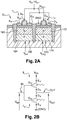
- FIG. 2A-2B A first example of configuration of a CMOS photosensitive logic inverter formed from the cell of the figure 1 , is given on figures 2A-2B , while the figures 2C-2D serve to illustrate the operation of this inverter.
- the logic state of a signal V OUT emitted at the output of the inverter depends on the quantity of photons received by the photosensitive zone opposite the first transistor T 1 and the second transistor T 2 .
- the logic inverter comprises a terminal IN connected to the respective gates G P and G N of the first transistor T 1 and of the second transistor T 2 , the gates G P and G N being connected to each other.
- An output OUT of the inverter making it possible to deliver the logic or binary signal V OUT , is connected to the respective drains D P and D N of the first transistor T 1 and of the second transistor T 2 , the drains D P and D N being connected between them ( figure 2B ).
- the device also comprises a means for biasing the source of the first transistor T 1 provided to apply a potential V DD to the source S P, for example of the order of 1V for transistors having a gate length of between 30 and 35 nm , or 0.9V for transistors having a gate length between 26 nm and 32 nm, or 0.75V for transistors having a gate length between 18 nm and 24 nm.
- a means for biasing the source of the first transistor T 1 provided to apply a potential V DD to the source S P, for example of the order of 1V for transistors having a gate length of between 30 and 35 nm , or 0.9V for transistors having a gate length between 26 nm and 32 nm, or 0.75V for transistors having a gate length between 18 nm and 24 nm.
- the source S N of the second transistor T 2 can be placed at a reference potential V SS or GND serving as ground.
- the transistors T 1 and T 2 are in this example biased so as to have a constant gate-source voltage V GS , the change of conduction state on or off of the transistors being obtained by shifting their threshold voltages V TN , V TP respective due to a variation in illumination of the photosensitive zone.
- Means for polarizing respectively the first junction 160 and the second junction 170 are also provided. These biasing means are configured to apply a first potential Vpoll, for example of the order of -5V to 5V to the lower doped zone 162 (in this example N-doped) of the first junction 160 and to apply a second potential Vpol2, for example of the order of -5V to 5V at the lower doped zone 172 (in this N doped example) of the second junction 170 while the respective upper doped zones of the junctions 160, 170 (in this example the zones 164, 174 doped P) are set to a floating potential.
- Vpoll for example of the order of -5V to 5V
- Vpol2 for example of the order of -5V to 5V
- Vpol2 for example of the order of -5V to 5V at the lower doped zone 172 (in this N doped example) of the second junction 170 while the respective upper doped zones of the junctions 160, 170 (in this example the zones 164, 174 do
- the amplitude of the threshold voltage shift induced by the LIVS light depends for each transistor on a ratio called “Body Factor”. »Capacitance between its channel and a region of the photosensitive zone playing the role of a back gate,
- the Body Factor depends on the bias potential applied (respectively Vpol1 for the first transistor and Vpol2 for the second transistor) to the zones spiked lower 172, 174.
- Provision can for example be made to apply the same bias potential Vpol1 Vpol2 to the lower doped zone 162 and to the lower doped zone 172.
- Vpol 1 and Vpol 2 can be applied respectively to the lower doped zone 162 and to the lower doped zone 172, so as to implement a threshold voltage shift induced by the light LIVS P for the first P-type transistor different from the LIVS N light-induced threshold voltage offset for the second N-type transistor.
- Vpoll, Vpol2 applied to control the threshold voltage shift LIVS depends on the direction of the junction (P / N or N / P), under the insulating layer of BOX on which the channels of the transistors rest.
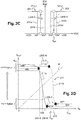
- curves 201, 202 of respective variations of the drain-source currents of the first transistor T 1 and of the second transistor T 2 as a function of their respective gate-source voltages are given.
- This figure shows shifts in threshold voltages LIVS P of the first transistor T 1 and LIVS N of the second transistor T 2 generated by the reception of a given quantity of photons or by a given increase in a quantity of photons received by the zone photosensitive arranged opposite the transistors T 1 , T 2 .
- the threshold voltage of the first transistor T 1 is liable to change from a value Vtp when the photosensitive zone is not illuminated or insufficiently illuminated (portion 201a of the curve 201 in continuous line) to a value Vtp * when the photosensitive zone is illuminated or sufficiently illuminated (portion 201b of curve 201 in broken line), with
- can be increased by decreasing the thickness e 2 of the insulating layer 101 of the weaker substrate, and / or by increasing the chosen thickness e 3 of the surface semiconductor layer, and / or by increasing the chosen thickness of the dielectric gate of the first transistor T 1 .
- the threshold voltage of the second transistor T 2 is liable to change from a value Vtn when the photosensitive zone is not illuminated or is insufficiently illuminated (portion 202a of the curve 202 in solid lines) to a value Vtn * when the photosensitive zone is illuminated or sufficiently illuminated (portion 202b of the curve 202 in broken lines), with Vtn * -Vtn which can be for example of the order of 100 mV.
- the arrangement of the P and N doped zones of the junctions 160, 170 is such that a change in illumination of the photosensitive zone causes a shift of the respective threshold voltages Vtn and Vtp of the transistors in the same one. direction of variation (VtN increasing and VtP decreasing in absolute value).
- VtN increasing and VtP decreasing in absolute value
- an increase in the quantity of photons received by the photosensitive zone of the logic inverter is here likely to induce a decrease (in absolute value) in the threshold voltage of the first transistor T 1 (of type P) and an increase of the threshold voltage of the second transistor T 2 (of type N).
- the 2D figure illustrates a transfer function of the output signal V OUT as a function of the signal applied to the input of the first example of a logic inverter when the latter is subjected to light radiation (portion of curve 211a) and when the latter is not subjected to light radiation (portion of curve 211b).
- the bias potential V NP is in this example chosen so as to be greater than a potential V M corresponding to the potential for which the potential V OUT at the output OUT of the inverter is equal to the potential V IN applied to the terminal IN.
- the bias potential V NP is preferably chosen such that V NP is greater than V M + ⁇ with ⁇ a voltage dependent on the noise margin and which is a function of the voltage V DD .
- V IN V NP applied to the terminal IN is advantageously chosen such that: V M + ⁇ ⁇ V NP ⁇ V M + ⁇ + LIVS NOT + LIVS P 2
- the bias potential V NP of the input IN can be chosen for example so that V NP ⁇ [VM; VM + 200 mV] V M depending on Vt N , Vtp, and on V DD .
- the first example of a photonic logic inverter can thus follow the following truth table: IN Light OUT V NP NO 0 V NP YES 1
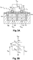
- FIG. 3A-3B A second example of a photosensitive logic inverter configuration is given on the figures 3A-3B , while the figures 3C-3D serve to illustrate how it works.
- the configuration of the second example of an inverter differs from that of the inverter described above in particular by the arrangement of the junctions 160, 170.
- the arrangement of the doped zones 162, 164 forming the first junction 160 is in this example ( figure 3A ) such that the P-doped zone 164 is arranged between the channel zone 104 of the first transistor T 1 and the N-doped zone 162.
- the arrangement of the doped zones 172, 174 forming the second junction 170 is itself such that the zone 174 P doped is disposed between the channel zone 124 of the second transistor T 2 and the second N doped zone 172.
- the second P-doped zones 164, 174 form in this example the upper zones of the junctions, while the N-doped zones 162, 172 form the lower zones of the junctions.
- Polarization means respectively of the first junction 160 and of the second junction 170 may be provided to apply a first potential Vpol 1 to the lower doped zone 162 (in this example doped N) of the first junction 160 and a second potential Vpol 2 to the lower doped zone 172 (in this example doped N) of the second junction 170, while the respective upper doped zones of the junctions 160, 170 in this example the P-doped zones 164, 174 of the junctions are set to a floating potential.
- the configuration of the second example of an inverter is similar to that of the first example of an inverter described above.
- the transistors T 1 and T 2 are thus biased so as to have a constant gate-source voltage V GS , a respective change of on or off state of the transistors being able to be obtained by varying their respective threshold voltages V TP and V TN. , this variation being itself dependent on the state of illumination of the photosensitive zone.
- the figure 3C gives variation curves 301, 302 of the respective drain-source currents of the first transistor T 1 and of the second transistor T 2 as a function of their respective gate-source voltages. It shows LIVS P and LIVS N offsets (illustrated respectively by an offset between the curve portion 301a and the curve portion 301b for the P-type transistor and by an offset between the curve portion 302a and the curve portion 302b for the N-type transistor) of the respective threshold voltages of the first transistor and of the second transistor generated by an illumination or an increase in illumination of the photosensitive zone.
- the threshold voltage of the first transistor T 1 (of type P) increases in absolute value, while the threshold voltage of the second transistor T 2 (of type N) decreases in absolute value.
- the threshold voltage shift Vt is done here in the same direction (negative).
- the input IN of the inverter is biased to a potential V Fixed PN chosen from a range (portion 310 on the abscissa axis of the 3d figure ) of suitable voltages.
- the bias potential V PN is in this example chosen so as to be less than the potential V M and preferably such that V PN is less than V M - ⁇ with ⁇ a voltage dependent on the noise margin.
- V PN applied to the terminal IN is advantageously chosen such that: For a BOX / P / N arrangement of the doped zones of the junctions as illustrated on the figure 3A , we define V PN by: V M - ⁇ - LIVS P + LIVS NOT 2 ⁇ V PN ⁇ V M - ⁇ with LIVS P > 0 and LIVSN ⁇ 0.
- the second example of a photonic logic inverter can thus follow the following truth table: IN Light OUT V NP NO 1 V NP YES 0
- photosensitive cells as described above, it is possible to implement a logic circuit capable of being controlled by light and whose functions, in particular logic, can be modified as a function of the level of illumination that this logic circuit receives.
- the 2D figures and 3d show that, in a certain voltage range applied to the input IN of a photosensitive logic inverter, it is possible to switch, by a variation in illumination and a sufficient supply of photons, the logic output OUT of the inverter, the logic state of this output OUT not switching when the supply of photons is insufficient.
- the function which can be modified by lighting can be, for example, a function of collective programming of cells or of reset.
- Such a logic circuit can be implemented, for example, so that a brief light pulse or a light flash makes it possible to switch a set of photosensitive logic inverters.
- a logic circuit controlled, or programmed, or reset, without requiring specific addressing, by means of a light flash applied for example to the rear face of a chip on which this circuit is mounted can thus be produced.
- a photosensitive logic inverter configuration variant is given on the figures 4A-4B , the figures 4C-4E used to illustrate its operation.
- the logic state '1' or '0' of the output signal V OUT of the inverter does not depend here, unlike the examples previously described, on the quantity of photons received by the photosensitive zone in other words on the 'illumination state of the latter, but of a logic state' 0 'or' 1 'of an electrical input signal V IN applied to input IN of the inverter.
- this photosensitive logic inverter configuration variant differs from the examples described above by the type of signal V IN applied to input IN ( figure 4B ), this signal being a variable voltage, capable of adopting at least a first value for which the transistor T 1 of type P is off while the transistor T 2 of type N is on, and at least a second value for which the transistor T 1 of type P is on while the transistor T 2 of type N is blocked.
- This third example of an inverter also differs from those described above by the arrangement of the junctions 160, 170.
- the arrangement of the doped areas 162, 164 forming the first junction 160 is such that the P-doped area 164 is disposed on the N-doped area 162, while that of the second junction 170 is such that the N-doped area 172 is disposed on P-doped zone 174 ( figure 4A ).
- curves 401, 402 of respective variations of the drain-source currents of the first transistor T 1 and of the second transistor T 2 as a function of their respective gate-source voltages are given.
- an increase in the quantity of photons received by the photosensitive zone is capable of generating an increase in the threshold voltage of the second transistor T 2, this increase being reflected by a shift between a portion of curve 402a in solid line illustrating a non-illuminated state of the photosensitive area and a portion of curve 402b in broken lines illustrating an illuminated state of the photosensitive area.
- an increase in the quantity of photons received by the photosensitive zone is capable of generating an increase (in absolute value) in the threshold voltage of the first transistor T 1 .
- the photosensitive logic inverter has a transfer function of a conventional inverter when it does not receive light radiation.
- the speed of transition at output OUT from one logic state to another logic state then results in a given slope of the portion of curve 411 on the figure 4D .
- the speed of transition from one logic state to another logic state is in this case greater, which results in a slope of the portion of curve 412 on the figure 4D higher than that of the curve portion 411.
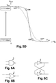
- FIGS. 5A-5D serve to illustrate another example of a photosensitive logic inverter configuration which differs from the example previously described in particular by the arrangement of the junctions 160, 170 ( figure 5A ).
- the arrangement of the doped zones 162, 164 forming the first junction 160 is such that the N-doped zone 162 is disposed between the channel zone 104 of the first transistor T 1 and the P-doped zone 164.
- doped areas 172, 174 forming the second junction 170 is for its part such that the P-doped area 174 is disposed between the channel area 124 of the second transistor T 2 and the N-doped area 172.
- the figure 5C gives curves 501, 502 of respective variations of the drain-source currents of the first transistor T 1 and of the second transistor T 2 as a function of their gate-source voltages and shows that an increase in the quantity of photons received by the photosensitive zone is capable of generating a decrease (in absolute value) in the threshold voltage of the first transistor T 1 (decrease reflected by a shift between a portion of curve 501a in solid line illustrating a non-illuminated state of the photosensitive zone and a portion of curve 501b in dashed line illustrating an illuminated state of the photosensitive zone) while a decrease in the threshold voltage of the second transistor T 2 (decrease reflected by a shift between a portion of curve 501a in solid line illustrating a non-illuminated state of the photosensitive zone and a portion of curve 502b in broken lines illustrating an illuminated state of the photosensitive zone).
- the switching speed from one logic state to another logic state at output OUT depends on the illumination state of the photosensitive zone ( figure 5D ).
- a photosensitive logic inverter matrix arrangement according to one or the other of the embodiments described above can be provided.
- a photosensitive logic inverter according to one or other of the configurations described above, it is also possible to implement a logic circuit comprising at least one logic gate requiring a logic function. inverting or "NOT”, for example a logic gate “NAND” ( figure 6A ) photosensitive or “NO OR” photosensitive ( figure 6B ).
- NOT for example a logic gate “NAND” ( figure 6A ) photosensitive or “NO OR” photosensitive
- a photosensitive logic inverter can also be integrated in a circuit forming a photosensitive latch ( figure 6C ), for example an SRAM memory switch.
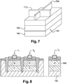
- the figure 8 illustrates an exemplary embodiment of the first P-type transistor T 1 of the photosensitive logic cell according to such finFET technology.
- the junction 160 formed of the superimposed N-doped zone 162 and of the P-doped zone 164 extends in the support layer facing a portion of the semiconductor bar 704 covered by the gate 710 and intended to form a channel.
- a photosensitive logic inverter as described above can be integrated within a device comprising one or more other transistors, for example transistors of a processing circuit, the threshold voltage of which does not vary or varies little as a function of light radiation received by an area of the support layer located opposite the latter.
- FIG 8 an example of such a device is illustrated and comprises a transistor T 3 juxtaposed with transistors T 1 and T 2 forming a photosensitive logic cell opposite which a single doped zone 895 is provided in a region of the support layer 100.
- This doped zone 895 for example of type P and to which a polarization potential can be applied, forms a ground plane ("ground plane" according to the English terminology) replacing the photosensitive zone, in order to make the transistor T 3 insensitive to light radiation.
- a photosensitive logic inverter according to the invention can be integrated into a device comprising several levels of superimposed transistors.
- FIG 9 an example of such a device is illustrated and comprises a transistor T 3, for example of a processing circuit located at a given level N k of a plurality of levels of superimposed components, while the transistors forming the logic inverter photosensitive (only the P-type transistor T 1 being illustrated in this figure) are located at a higher level N k + 1 .
- transistor T 3 may be insensitive to light radiation, so that its threshold voltage does not vary or varies little as a function of the quantity of photons received by the device.
- the channel zone of transistor T 3 is not located opposite a junction capable of acting on its threshold voltage.
- the creation of defects by implantation in the junctions may possibly make it possible to facilitate this discharge.
- Another way to allow rapid discharge of the BOX / junction interface without modifying the structure of the cells is to provide a cell (s) polarization control circuit configured to emit a specific initialization pulse or erasure.
- This pulse is in the form of a voltage step or an edge whose direction of variation depends on the type of PN or NP junction located under the insulating layer of BOX.
- This initialization or erasure pulse can be applied to the respective gates of the transistors of the cell located opposite the junctions and transmitted by electrostatic or capacitive coupling.
- the initialization or erasure pulse can be emitted periodically during an initialization or erasure phase scheduled during each cycle of the photosensitive logic cell and can precede or follow each reading phase in which the logic state of the cell is read.
- an example of the operating sequence of a matrix of photosensitive logic cells comprises an initialization phase of the matrix, then a waiting phase, for example of the order of several nanoseconds during which the cells illuminated are loaded, then a reading phase. Then, such a sequence is repeated.
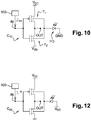
- the figure 10 illustrates an example of a device provided with such a polarization control circuit 100 adapted to a photosensitive logic cell C 10 .
- This C 10 cell has a junction configuration similar to that of the cell previously described in connection with the figures 3A and 3B , that is to say with P-doped areas arranged on the N-doped areas and thus interposed between the N-doped areas and the BOX insulating layer.
- the representation used to show the coupling effect between the front face and the rear face of the substrate is such that the transistors are shown with a second gate on the rear face, the junctions being symbolized by a PD photodiode.
- the voltage step emitted by circuit 100 to allow the discharge at the BOX / junction interface to be accelerated is a voltage step positive, applied to the IN terminal connected to the gates of transistors T 1 and T 2 of cell C 20 .
- the amplitude of the step depends in particular on the type of transistors and on the technology in which the transistors of the cell are made.
- the respective sources of transistors T 1 , T 2 can advantageously be placed by the bias control circuit 100 at a ground potential GND in order to minimize the leaks.
- the bias control circuit 100 applies an ascending voltage step to the gate of transistors T 1 and T 2 of cell C 10 .
- a step can also be applied to the source and drain regions of transistors T 1 , T 2 .
- Such a step can also be applied to a gate of transistors T 1 , T 2 placed on the rear face and interposed between the junction and the insulating layer of BOX.
- the figures 11A-11B illustrate the effect of a voltage step ( figure 11B ) on the strip structure on the rear face of cell C 20 .
- the figure 12 illustrates an alternative embodiment suitable for a photosensitive logic cell C 20 , the configuration of which is similar to that described above in connection with the figures 2A and 2B , that is to say in which the N-doped areas of the junctions are arranged on the P-doped areas and are thus interposed between the P-doped areas and the BOX insulating layer.
- the voltage step emitted by circuit 100 to make it possible to accelerate the discharge at the BOX / junction interface is a voltage step descending, applied to the terminal IN connected to the respective gates of the first transistor T 1 and of the second transistor T 2 .
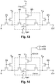
- a polarization control circuit using NMOS and PMOS transistors and configured to modify the polarization state of a photosensitive logic cell C 10 as described previously in connection with the figure 10 are given on figures 13 and 14 .
- the state of polarization of the photosensitive logic cell C 10 depends on the logic state of read signals RD and erase ER.
Landscapes
- Physics & Mathematics (AREA)
- General Physics & Mathematics (AREA)
- Nonlinear Science (AREA)
- Optics & Photonics (AREA)
- Metal-Oxide And Bipolar Metal-Oxide Semiconductor Integrated Circuits (AREA)
- Logic Circuits (AREA)
Claims (15)
- Vorrichtung mit zumindest einer lichtempfindlichen logischen Zelle, wobei die lichtempfindliche logische Zelle enthält:einen ersten Transistor (T1) des p-Typs und einen zweiten Transistor (T2) des n-Typs, die auf einem Halbleiter-auf-Isolator-Substrat aufliegen, wobei das Substrat eine oberflächliche Halbleiterschicht (102) mit einem Kanalbereich des ersten Transistors und einem Kanalbereich des zweiten Transistors, undeine Isolierschicht (101), die die oberflächliche Halbleiterschicht (102) von einer Halbleiterträgerschicht (100) trennt, aufweist, wobei die Isolierschicht (101) auf einer sogenannten "Vorderseite" der Halbleiterträgerschicht (100) aufliegt, die einer sogenannten "Rückseite" der Halbleiterträgerschicht (100) entgegengesetzt ist,wobei die Halbleiterträgerschicht mindestens einen lichtempfindlichen Bereich (150) enthält, wobei der lichtempfindliche Bereich (150) dazu ausgelegt ist, Photonen, die an der Rückseite der Trägerschicht (100) eindringen, in Ladungsträger umzuwandeln, und einen ersten Übergang (160), der dem Kanalbereich des ersten Transistors (T1) gegenüberliegend angeordnet ist,und einen zweiten Übergang (170) aufweist, der dem Kanalbereich des zweiten Transistors (T2) gegenüberliegend angeordnet ist, wobei die Isolierschicht dazu ausgelegt ist, eine kapazitive Kopplung zwischen dem lichtempfindlichen Bereich und der oberflächlichen Halbleiterschicht zu ermöglichen, so dass der erste Transistor und der zweite Transistor jeweils eine erste Schwellenspannung (VTP) bzw. eine zweite Schwellenspannung (VTN) aufweisen, die in Abhängigkeit von einer von dem lichtempfindlichen Bereich empfangenen Photonenmenge moduliert werden können,wobei der erste Transistor und der zweite Transistor so angeordnet sind, dass sie einen logischen Inverter bilden.
- Vorrichtung nach Anspruch 1, wobei der erste Übergang (160) und der zweite Übergang (170) enthalten:- jeweils einen n-dotierten unteren Bereich (162, 172), der von einem p-dotierten oberen Bereich (164, 174) überragt wird, oder- jeweils einen unteren p-dotierten Bereich (164, 174), der von einem oberen n-dotierten Bereich (162, 172) überlagert wird.
- Vorrichtung nach Anspruch 2, ferner enthaltend:- Mittel zum Vorspannen des ersten Transistors und des zweiten Transistors, um an einen Eingang (IN), der mit den Gates (Gp, GN) des ersten und des zweiten Transistors verbunden ist, ein vorbestimmtes festes Vorspannungspotential (VPN, VNP) anzulegen, wobei der erste Transistor und der zweite Transistor so vorgespannt werden, dass sie jeweils konstante Gate-Source-Spannungen haben.
- Vorrichtung nach einem der Ansprüche 2 oder 3, wobei der Inverter dazu ausgelegt ist, an seinem Ausgang einen ersten logischen Zustand anzunehmen, der einen ersten Beleuchtungszustand des lichtempfindlichen Bereichs durch Lichtstrahlung widergibt, und an seinem Ausgang einen zweiten logischen Zustand anzunehmen, der sich von dem ersten Zustand unterscheidet und einen zweiten Beleuchtungszustand des lichtempfindlichen Bereichs widergibt, der sich von dem ersten Beleuchtungszustand unterscheidet.
- Vorrichtung nach Anspruch 1, wobei der erste Übergang (160) einen unteren n-dotierten Bereich (162) aufweist, der von einem oberen p-dotierten Bereich (164) überragt wird, wobei der zweite Übergang einen unteren p-dotierten Bereich (174) aufweist, der von einem oberen n-dotierten Bereich (172) überragt wird, oder
wobei der erste Übergang (160) einen unteren p-dotierten Bereich (164) aufweist, der von einem oberen n-dotierten Bereich (162) überragt wird, wobei der zweite Übergang einen unteren n-dotierten Bereich (172) aufweist, der von einem oberen p-dotierten Bereich (174) überragt wird. - Vorrichtung nach Anspruch 5, enthaltend Mittel zum Anlegen eines variablen Potentials (VIN) an den Eingang (IN) des Inverters.
- Vorrichtung nach einem der Ansprüche 1 bis 6, ferner enthaltend Polarisationsmittel, die dazu ausgelegt sind, ein bestimmtes Polarisationspotential (Vpol1, Vpol2) an den unteren Bereich des ersten Übergangs (160) und/oder des zweiten Übergangs (170) anlegen, wobei der obere Bereich des ersten Übergangs (160) und/oder des zweiten Übergangs (170) auf ein schwebendes Potential gesetzt ist.
- Vorrichtung nach einem der Ansprüche 1 bis 7, ferner enthaltend zumindest einen isolierenden Graben (181) zwischen dem ersten Transistor (T1) und dem zweiten Transistor (T2), wobei der isolierende Graben (181) durch die Trägerschicht hindurchgeht und dazu ausgelegt ist, einen oberen dotierten Bereich des ersten Übergangs (160) von einem oberen dotierten Bereich des zweiten Übergangs (170) elektrisch zu isolieren.
- Vorrichtung nach einem der Ansprüche 1 bis 8, ferner enthaltend zumindest einen isolierenden Bereich (183, 185) um den ersten Transistor und/oder den zweiten Transistor herum, wobei der isolierende Bereich durch die Trägerschicht hindurchgeht und dazu ausgelegt ist, die Zelle von einer anderen Zelle oder einem anderen auf dem Substrat gebildeten Element elektrisch zu isolieren.
- Vorrichtung nach einem der Ansprüche 1 bis 9, ferner enthaltend zumindest einen weiteren Transistor (T3), der neben der logischen Zelle angeordnet ist, wobei dem weiteren Transistor gegenüberliegend eine Masseebene in der Halbleiterträgerschicht vorgesehen ist.
- Vorrichtung nach einem der Ansprüche 1 bis 10, ferner enthaltend zumindest einen weiteren Transistor (T3), der der logischen Zelle überlagert ist.
- Vorrichtung nach einem der Ansprüche 1 bis 11, wobei die logische Zelle zu einer logischen Schaltung zum Ausführen einer bestimmten logischen Funktion, wie etwa einer NAND- oder NOR-Funktion, gehört.
- Vorrichtung nach einem der Ansprüche 1 bis 11, wobei die lichtempfindliche logische Zelle zu einer SRAM-Speicherzelle gehört.
- Lichtempfindliche logische Schaltung, die eine gegebene logische Funktion ausführt und mit einer oder mehreren Vorrichtungen nach einem der Ansprüche 1 bis 13 versehen ist, wobei die Funktion in Abhängigkeit von der Beleuchtung der Vorrichtunge(en) veränderbar ist.
- Vorrichtung nach einem der Ansprüche 1 bis 14, ferner enthaltend eine Vorspannungssteuerschaltung, die dazu ausgelegt ist, den Vorspannungszustand des ersten und des zweiten Transistors zu ändern und eine Spannungsstufe an den ersten Transistor und an den zweiten Transistor anzulegen, um eine Entladung von Bereichen an der Grenzfläche zwischen der Isolierschicht und dem ersten bzw. zweiten Übergang zu ermöglichen.
Applications Claiming Priority (1)
| Application Number | Priority Date | Filing Date | Title |
|---|---|---|---|
| FR1454686A FR3021458B1 (fr) | 2014-05-23 | 2014-05-23 | Inverseur cmos photonique |
Publications (3)
| Publication Number | Publication Date |
|---|---|
| EP2947689A2 EP2947689A2 (de) | 2015-11-25 |
| EP2947689A3 EP2947689A3 (de) | 2016-02-24 |
| EP2947689B1 true EP2947689B1 (de) | 2020-08-19 |
Family
ID=51352616
Family Applications (1)
| Application Number | Title | Priority Date | Filing Date |
|---|---|---|---|
| EP15168852.0A Not-in-force EP2947689B1 (de) | 2014-05-23 | 2015-05-22 | Photonischer cmos-wechselrichter |
Country Status (3)
| Country | Link |
|---|---|
| US (1) | US9841657B2 (de) |
| EP (1) | EP2947689B1 (de) |
| FR (1) | FR3021458B1 (de) |
Families Citing this family (6)
| Publication number | Priority date | Publication date | Assignee | Title |
|---|---|---|---|---|
| US9874693B2 (en) | 2015-06-10 | 2018-01-23 | The Research Foundation For The State University Of New York | Method and structure for integrating photonics with CMOs |
| FR3043249B1 (fr) | 2015-10-28 | 2018-03-09 | Commissariat A L'energie Atomique Et Aux Energies Alternatives | Cellule logique photosensible a illumination par la face avant |
| FR3070792A1 (fr) | 2017-09-05 | 2019-03-08 | Commissariat A L'energie Atomique Et Aux Energies Alternatives | Detecteur photosensible a jonction 3d et grille autoalignees |
| CN111063702B (zh) * | 2019-11-13 | 2022-10-04 | 北京大学 | 一种utbb光电探测器像素单元、阵列和方法 |
| US20250006749A1 (en) * | 2022-08-17 | 2025-01-02 | Peking University | Image sensing computing unit and its operating method, image sensing computer and electronic device |
| CN119483585B (zh) * | 2024-11-20 | 2025-10-21 | 北京纳米能源与系统研究所 | 基于可重构晶体管构建的类cmos反相器及其调制方法 |
Family Cites Families (11)
| Publication number | Priority date | Publication date | Assignee | Title |
|---|---|---|---|---|
| JP2594992B2 (ja) * | 1987-12-04 | 1997-03-26 | 株式会社日立製作所 | 固体撮像装置 |
| US7498644B2 (en) * | 2002-06-04 | 2009-03-03 | Nds Limited | Prevention of tampering in electronic devices |
| GB2389960A (en) * | 2002-06-20 | 2003-12-24 | Suisse Electronique Microtech | Four-tap demodulation pixel |
| US6845034B2 (en) * | 2003-03-11 | 2005-01-18 | Micron Technology, Inc. | Electronic systems, constructions for detecting properties of objects, and assemblies for identifying persons |
| US7875958B2 (en) * | 2006-09-27 | 2011-01-25 | Taiwan Semiconductor Manufacturing Company, Ltd. | Quantum tunneling devices and circuits with lattice-mismatched semiconductor structures |
| JP4215806B2 (ja) * | 2007-03-30 | 2009-01-28 | 株式会社東芝 | 半導体装置 |
| US7759714B2 (en) * | 2007-06-26 | 2010-07-20 | Hitachi, Ltd. | Semiconductor device |
| FR2932005B1 (fr) * | 2008-06-02 | 2011-04-01 | Commissariat Energie Atomique | Circuit a transistor integres dans trois dimensions et ayant une tension de seuil vt ajustable dynamiquement |
| US9054221B2 (en) * | 2011-08-31 | 2015-06-09 | Institute of Microelectronics, Chinese Academy of Sciences | Semiconductor device with a common back gate isolation region and method for manufacturing the same |
| FR2982079A1 (fr) * | 2011-10-28 | 2013-05-03 | Commissariat Energie Atomique | Imageur cmos utbb |
| FR3009887B1 (fr) | 2013-08-20 | 2015-09-25 | Commissariat Energie Atomique | Procede ameliore de separation entre une zone active d'un substrat et sa face arriere ou une portion de sa face arriere |
-
2014
- 2014-05-23 FR FR1454686A patent/FR3021458B1/fr not_active Expired - Fee Related
-
2015
- 2015-05-22 EP EP15168852.0A patent/EP2947689B1/de not_active Not-in-force
- 2015-05-22 US US14/719,580 patent/US9841657B2/en not_active Expired - Fee Related
Non-Patent Citations (1)
| Title |
|---|
| None * |
Also Published As
| Publication number | Publication date |
|---|---|
| FR3021458B1 (fr) | 2016-07-01 |
| FR3021458A1 (fr) | 2015-11-27 |
| US9841657B2 (en) | 2017-12-12 |
| EP2947689A3 (de) | 2016-02-24 |
| US20150338720A1 (en) | 2015-11-26 |
| EP2947689A2 (de) | 2015-11-25 |
Similar Documents
| Publication | Publication Date | Title |
|---|---|---|
| EP2947689B1 (de) | Photonischer cmos-wechselrichter | |
| FR2953641A1 (fr) | Circuit de transistors homogenes sur seoi avec grille de controle arriere enterree sous la couche isolante | |
| EP2587539B1 (de) | CMOS-UTBB-Bildaufnehmer | |
| EP2415079B1 (de) | Integrierter soi-schaltkreis mit transistoren mit separaten schwellenspannungen | |
| EP2750180B1 (de) | Integrierter Schaltkreis, der eine Taktbaumzelle umfasst | |
| FR2980035A1 (fr) | Circuit integre realise en soi comprenant des cellules adjacentes de differents types | |
| FR2958441A1 (fr) | Circuit pseudo-inverseur sur seoi | |
| FR2558010A1 (fr) | Procede pour la fabrication de transistors mos complementaires a basses tensions de seuil dans des circuits integres a haute densite et structure resultant de ce procede | |
| WO2003088366A1 (fr) | Dispositif semiconducteur de memoire, non volatile, programmable et effacable electriquement, a une seule couche de materiau de grille, et plan memoire correspondant | |
| EP1873836B1 (de) | Von hinten beleuchtete Bildaufnahmevorrichtung | |
| EP2685501A1 (de) | Integrierter SOI-Schaltkreis, der einen darunterliegenden Schutztransistor umfasst | |
| FR3007577A1 (fr) | Transistors avec differents niveaux de tensions de seuil et absence de distorsions entre nmos et pmos | |
| FR3003996A1 (fr) | Procede de commande d'un circuit integre | |
| EP2685499A1 (de) | Integrierter SOI-Schaltkreis, der einen Triac zum Schutz gegen elektrostatische Entladungen umfasst | |
| FR2689683A1 (fr) | Dispositif semiconducteur à transistors complémentaires. | |
| EP2200083A2 (de) | Halbleiterdetektor mit schwebendem Gate | |
| EP3451340B1 (de) | Programmierungsverfahren einer dram-speicherzelle mit einem transistor, und speichervorrichtung | |
| EP1107314A1 (de) | Strahlenfester MOS-Transistor | |
| EP2750179B1 (de) | Integrierter Schaltkreis, der eine Taktbaumzelle umfasst | |
| EP3163622B1 (de) | Lichtempfindliche logikzelle zur beleuchtung von der vorderseite | |
| EP0098191B1 (de) | Optoelektronischer Sensor mit Überlaufvorrichtung | |
| FR2846147A1 (fr) | Commande d'une cellule photosensible | |
| WO2014057112A1 (fr) | Circuit integre comportant des transistors avec des tensions de seuil differentes | |
| FR2934926A1 (fr) | Capteur d'images miniature. | |
| EP1876647A2 (de) | Rückbeleuchteter Bildsensor |
Legal Events
| Date | Code | Title | Description |
|---|---|---|---|
| PUAI | Public reference made under article 153(3) epc to a published international application that has entered the european phase |
Free format text: ORIGINAL CODE: 0009012 |
|
| AK | Designated contracting states |
Kind code of ref document: A2 Designated state(s): AL AT BE BG CH CY CZ DE DK EE ES FI FR GB GR HR HU IE IS IT LI LT LU LV MC MK MT NL NO PL PT RO RS SE SI SK SM TR |
|
| AX | Request for extension of the european patent |
Extension state: BA ME |
|
| PUAL | Search report despatched |
Free format text: ORIGINAL CODE: 0009013 |
|
| AK | Designated contracting states |
Kind code of ref document: A3 Designated state(s): AL AT BE BG CH CY CZ DE DK EE ES FI FR GB GR HR HU IE IS IT LI LT LU LV MC MK MT NL NO PL PT RO RS SE SI SK SM TR |
|
| AX | Request for extension of the european patent |
Extension state: BA ME |
|
| RIC1 | Information provided on ipc code assigned before grant |
Ipc: H01L 27/144 20060101AFI20160115BHEP Ipc: H01L 21/84 20060101ALI20160115BHEP Ipc: H01L 27/12 20060101ALI20160115BHEP |
|
| 17P | Request for examination filed |
Effective date: 20160823 |
|
| RBV | Designated contracting states (corrected) |
Designated state(s): AL AT BE BG CH CY CZ DE DK EE ES FI FR GB GR HR HU IE IS IT LI LT LU LV MC MK MT NL NO PL PT RO RS SE SI SK SM TR |
|
| STAA | Information on the status of an ep patent application or granted ep patent |
Free format text: STATUS: REQUEST FOR EXAMINATION WAS MADE |
|
| R17P | Request for examination filed (corrected) |
Effective date: 20160823 |
|
| STAA | Information on the status of an ep patent application or granted ep patent |
Free format text: STATUS: EXAMINATION IS IN PROGRESS |
|
| 17Q | First examination report despatched |
Effective date: 20190508 |
|
| GRAP | Despatch of communication of intention to grant a patent |
Free format text: ORIGINAL CODE: EPIDOSNIGR1 |
|
| STAA | Information on the status of an ep patent application or granted ep patent |
Free format text: STATUS: GRANT OF PATENT IS INTENDED |
|
| RIC1 | Information provided on ipc code assigned before grant |
Ipc: H01L 27/12 20060101ALI20200211BHEP Ipc: H01L 27/144 20060101AFI20200211BHEP Ipc: G02F 3/02 20060101ALI20200211BHEP Ipc: H01L 21/84 20060101ALI20200211BHEP |
|
| INTG | Intention to grant announced |
Effective date: 20200310 |
|
| GRAS | Grant fee paid |
Free format text: ORIGINAL CODE: EPIDOSNIGR3 |
|
| GRAA | (expected) grant |
Free format text: ORIGINAL CODE: 0009210 |
|
| STAA | Information on the status of an ep patent application or granted ep patent |
Free format text: STATUS: THE PATENT HAS BEEN GRANTED |
|
| AK | Designated contracting states |
Kind code of ref document: B1 Designated state(s): AL AT BE BG CH CY CZ DE DK EE ES FI FR GB GR HR HU IE IS IT LI LT LU LV MC MK MT NL NO PL PT RO RS SE SI SK SM TR |
|
| REG | Reference to a national code |
Ref country code: CH Ref legal event code: EP |
|
| REG | Reference to a national code |
Ref country code: DE Ref legal event code: R096 Ref document number: 602015057604 Country of ref document: DE |
|
| REG | Reference to a national code |
Ref country code: AT Ref legal event code: REF Ref document number: 1304915 Country of ref document: AT Kind code of ref document: T Effective date: 20200915 |
|
| REG | Reference to a national code |
Ref country code: IE Ref legal event code: FG4D Free format text: LANGUAGE OF EP DOCUMENT: FRENCH |
|
| REG | Reference to a national code |
Ref country code: LT Ref legal event code: MG4D |
|
| REG | Reference to a national code |
Ref country code: NL Ref legal event code: MP Effective date: 20200819 |
|
| PG25 | Lapsed in a contracting state [announced via postgrant information from national office to epo] |
Ref country code: SE Free format text: LAPSE BECAUSE OF FAILURE TO SUBMIT A TRANSLATION OF THE DESCRIPTION OR TO PAY THE FEE WITHIN THE PRESCRIBED TIME-LIMIT Effective date: 20200819 Ref country code: BG Free format text: LAPSE BECAUSE OF FAILURE TO SUBMIT A TRANSLATION OF THE DESCRIPTION OR TO PAY THE FEE WITHIN THE PRESCRIBED TIME-LIMIT Effective date: 20201119 Ref country code: PT Free format text: LAPSE BECAUSE OF FAILURE TO SUBMIT A TRANSLATION OF THE DESCRIPTION OR TO PAY THE FEE WITHIN THE PRESCRIBED TIME-LIMIT Effective date: 20201221 Ref country code: NO Free format text: LAPSE BECAUSE OF FAILURE TO SUBMIT A TRANSLATION OF THE DESCRIPTION OR TO PAY THE FEE WITHIN THE PRESCRIBED TIME-LIMIT Effective date: 20201119 Ref country code: FI Free format text: LAPSE BECAUSE OF FAILURE TO SUBMIT A TRANSLATION OF THE DESCRIPTION OR TO PAY THE FEE WITHIN THE PRESCRIBED TIME-LIMIT Effective date: 20200819 Ref country code: GR Free format text: LAPSE BECAUSE OF FAILURE TO SUBMIT A TRANSLATION OF THE DESCRIPTION OR TO PAY THE FEE WITHIN THE PRESCRIBED TIME-LIMIT Effective date: 20201120 Ref country code: HR Free format text: LAPSE BECAUSE OF FAILURE TO SUBMIT A TRANSLATION OF THE DESCRIPTION OR TO PAY THE FEE WITHIN THE PRESCRIBED TIME-LIMIT Effective date: 20200819 Ref country code: LT Free format text: LAPSE BECAUSE OF FAILURE TO SUBMIT A TRANSLATION OF THE DESCRIPTION OR TO PAY THE FEE WITHIN THE PRESCRIBED TIME-LIMIT Effective date: 20200819 |
|
| REG | Reference to a national code |
Ref country code: AT Ref legal event code: MK05 Ref document number: 1304915 Country of ref document: AT Kind code of ref document: T Effective date: 20200819 |
|
| PG25 | Lapsed in a contracting state [announced via postgrant information from national office to epo] |
Ref country code: LV Free format text: LAPSE BECAUSE OF FAILURE TO SUBMIT A TRANSLATION OF THE DESCRIPTION OR TO PAY THE FEE WITHIN THE PRESCRIBED TIME-LIMIT Effective date: 20200819 Ref country code: PL Free format text: LAPSE BECAUSE OF FAILURE TO SUBMIT A TRANSLATION OF THE DESCRIPTION OR TO PAY THE FEE WITHIN THE PRESCRIBED TIME-LIMIT Effective date: 20200819 Ref country code: RS Free format text: LAPSE BECAUSE OF FAILURE TO SUBMIT A TRANSLATION OF THE DESCRIPTION OR TO PAY THE FEE WITHIN THE PRESCRIBED TIME-LIMIT Effective date: 20200819 Ref country code: NL Free format text: LAPSE BECAUSE OF FAILURE TO SUBMIT A TRANSLATION OF THE DESCRIPTION OR TO PAY THE FEE WITHIN THE PRESCRIBED TIME-LIMIT Effective date: 20200819 Ref country code: IS Free format text: LAPSE BECAUSE OF FAILURE TO SUBMIT A TRANSLATION OF THE DESCRIPTION OR TO PAY THE FEE WITHIN THE PRESCRIBED TIME-LIMIT Effective date: 20201219 |
|
| PG25 | Lapsed in a contracting state [announced via postgrant information from national office to epo] |
Ref country code: CZ Free format text: LAPSE BECAUSE OF FAILURE TO SUBMIT A TRANSLATION OF THE DESCRIPTION OR TO PAY THE FEE WITHIN THE PRESCRIBED TIME-LIMIT Effective date: 20200819 Ref country code: DK Free format text: LAPSE BECAUSE OF FAILURE TO SUBMIT A TRANSLATION OF THE DESCRIPTION OR TO PAY THE FEE WITHIN THE PRESCRIBED TIME-LIMIT Effective date: 20200819 Ref country code: SM Free format text: LAPSE BECAUSE OF FAILURE TO SUBMIT A TRANSLATION OF THE DESCRIPTION OR TO PAY THE FEE WITHIN THE PRESCRIBED TIME-LIMIT Effective date: 20200819 Ref country code: RO Free format text: LAPSE BECAUSE OF FAILURE TO SUBMIT A TRANSLATION OF THE DESCRIPTION OR TO PAY THE FEE WITHIN THE PRESCRIBED TIME-LIMIT Effective date: 20200819 Ref country code: EE Free format text: LAPSE BECAUSE OF FAILURE TO SUBMIT A TRANSLATION OF THE DESCRIPTION OR TO PAY THE FEE WITHIN THE PRESCRIBED TIME-LIMIT Effective date: 20200819 |
|
| REG | Reference to a national code |
Ref country code: DE Ref legal event code: R097 Ref document number: 602015057604 Country of ref document: DE |
|
| PG25 | Lapsed in a contracting state [announced via postgrant information from national office to epo] |
Ref country code: ES Free format text: LAPSE BECAUSE OF FAILURE TO SUBMIT A TRANSLATION OF THE DESCRIPTION OR TO PAY THE FEE WITHIN THE PRESCRIBED TIME-LIMIT Effective date: 20200819 Ref country code: AL Free format text: LAPSE BECAUSE OF FAILURE TO SUBMIT A TRANSLATION OF THE DESCRIPTION OR TO PAY THE FEE WITHIN THE PRESCRIBED TIME-LIMIT Effective date: 20200819 Ref country code: AT Free format text: LAPSE BECAUSE OF FAILURE TO SUBMIT A TRANSLATION OF THE DESCRIPTION OR TO PAY THE FEE WITHIN THE PRESCRIBED TIME-LIMIT Effective date: 20200819 |
|
| PLBE | No opposition filed within time limit |
Free format text: ORIGINAL CODE: 0009261 |
|
| STAA | Information on the status of an ep patent application or granted ep patent |
Free format text: STATUS: NO OPPOSITION FILED WITHIN TIME LIMIT |
|
| PG25 | Lapsed in a contracting state [announced via postgrant information from national office to epo] |
Ref country code: SK Free format text: LAPSE BECAUSE OF FAILURE TO SUBMIT A TRANSLATION OF THE DESCRIPTION OR TO PAY THE FEE WITHIN THE PRESCRIBED TIME-LIMIT Effective date: 20200819 |
|
| 26N | No opposition filed |
Effective date: 20210520 |
|
| PG25 | Lapsed in a contracting state [announced via postgrant information from national office to epo] |
Ref country code: IT Free format text: LAPSE BECAUSE OF FAILURE TO SUBMIT A TRANSLATION OF THE DESCRIPTION OR TO PAY THE FEE WITHIN THE PRESCRIBED TIME-LIMIT Effective date: 20200819 |
|
| PG25 | Lapsed in a contracting state [announced via postgrant information from national office to epo] |
Ref country code: SI Free format text: LAPSE BECAUSE OF FAILURE TO SUBMIT A TRANSLATION OF THE DESCRIPTION OR TO PAY THE FEE WITHIN THE PRESCRIBED TIME-LIMIT Effective date: 20200819 |
|
| REG | Reference to a national code |
Ref country code: CH Ref legal event code: PL |
|
| GBPC | Gb: european patent ceased through non-payment of renewal fee |
Effective date: 20210522 |
|
| PG25 | Lapsed in a contracting state [announced via postgrant information from national office to epo] |
Ref country code: MC Free format text: LAPSE BECAUSE OF FAILURE TO SUBMIT A TRANSLATION OF THE DESCRIPTION OR TO PAY THE FEE WITHIN THE PRESCRIBED TIME-LIMIT Effective date: 20200819 Ref country code: LI Free format text: LAPSE BECAUSE OF NON-PAYMENT OF DUE FEES Effective date: 20210531 Ref country code: LU Free format text: LAPSE BECAUSE OF NON-PAYMENT OF DUE FEES Effective date: 20210522 Ref country code: CH Free format text: LAPSE BECAUSE OF NON-PAYMENT OF DUE FEES Effective date: 20210531 |
|
| REG | Reference to a national code |
Ref country code: BE Ref legal event code: MM Effective date: 20210531 |
|
| PG25 | Lapsed in a contracting state [announced via postgrant information from national office to epo] |
Ref country code: IE Free format text: LAPSE BECAUSE OF NON-PAYMENT OF DUE FEES Effective date: 20210522 Ref country code: GB Free format text: LAPSE BECAUSE OF NON-PAYMENT OF DUE FEES Effective date: 20210522 |
|
| PG25 | Lapsed in a contracting state [announced via postgrant information from national office to epo] |
Ref country code: BE Free format text: LAPSE BECAUSE OF NON-PAYMENT OF DUE FEES Effective date: 20210531 |
|
| PG25 | Lapsed in a contracting state [announced via postgrant information from national office to epo] |
Ref country code: HU Free format text: LAPSE BECAUSE OF FAILURE TO SUBMIT A TRANSLATION OF THE DESCRIPTION OR TO PAY THE FEE WITHIN THE PRESCRIBED TIME-LIMIT; INVALID AB INITIO Effective date: 20150522 |
|
| PG25 | Lapsed in a contracting state [announced via postgrant information from national office to epo] |
Ref country code: CY Free format text: LAPSE BECAUSE OF FAILURE TO SUBMIT A TRANSLATION OF THE DESCRIPTION OR TO PAY THE FEE WITHIN THE PRESCRIBED TIME-LIMIT Effective date: 20200819 |
|
| PG25 | Lapsed in a contracting state [announced via postgrant information from national office to epo] |
Ref country code: MK Free format text: LAPSE BECAUSE OF FAILURE TO SUBMIT A TRANSLATION OF THE DESCRIPTION OR TO PAY THE FEE WITHIN THE PRESCRIBED TIME-LIMIT Effective date: 20200819 |
|
| PGFP | Annual fee paid to national office [announced via postgrant information from national office to epo] |
Ref country code: DE Payment date: 20240517 Year of fee payment: 10 |
|
| PGFP | Annual fee paid to national office [announced via postgrant information from national office to epo] |
Ref country code: FR Payment date: 20240523 Year of fee payment: 10 |
|
| PG25 | Lapsed in a contracting state [announced via postgrant information from national office to epo] |
Ref country code: MT Free format text: LAPSE BECAUSE OF FAILURE TO SUBMIT A TRANSLATION OF THE DESCRIPTION OR TO PAY THE FEE WITHIN THE PRESCRIBED TIME-LIMIT Effective date: 20200819 |
|
| REG | Reference to a national code |
Ref country code: DE Ref legal event code: R079 Ref document number: 602015057604 Country of ref document: DE Free format text: PREVIOUS MAIN CLASS: H01L0027144000 Ipc: H10F0039100000 |
|
| REG | Reference to a national code |
Ref country code: DE Ref legal event code: R119 Ref document number: 602015057604 Country of ref document: DE |
|
| PG25 | Lapsed in a contracting state [announced via postgrant information from national office to epo] |
Ref country code: TR Free format text: LAPSE BECAUSE OF FAILURE TO SUBMIT A TRANSLATION OF THE DESCRIPTION OR TO PAY THE FEE WITHIN THE PRESCRIBED TIME-LIMIT Effective date: 20200819 |
|
| PG25 | Lapsed in a contracting state [announced via postgrant information from national office to epo] |
Ref country code: DE Free format text: LAPSE BECAUSE OF NON-PAYMENT OF DUE FEES Effective date: 20251202 |
|
| PG25 | Lapsed in a contracting state [announced via postgrant information from national office to epo] |
Ref country code: FR Free format text: LAPSE BECAUSE OF NON-PAYMENT OF DUE FEES Effective date: 20250531 |