EP1109209A1 - Procédé de fabrication d'un réseau de lignes nanométriques en silicium monocristallin et dispositif obtenu - Google Patents
Procédé de fabrication d'un réseau de lignes nanométriques en silicium monocristallin et dispositif obtenu Download PDFInfo
- Publication number
- EP1109209A1 EP1109209A1 EP00403511A EP00403511A EP1109209A1 EP 1109209 A1 EP1109209 A1 EP 1109209A1 EP 00403511 A EP00403511 A EP 00403511A EP 00403511 A EP00403511 A EP 00403511A EP 1109209 A1 EP1109209 A1 EP 1109209A1
- Authority
- EP
- European Patent Office
- Prior art keywords
- silicon
- lines
- recess
- side walls
- monocrystalline silicon
- Prior art date
- Legal status (The legal status is an assumption and is not a legal conclusion. Google has not performed a legal analysis and makes no representation as to the accuracy of the status listed.)
- Withdrawn
Links
Images
Classifications
-
- H—ELECTRICITY
- H10—SEMICONDUCTOR DEVICES; ELECTRIC SOLID-STATE DEVICES NOT OTHERWISE PROVIDED FOR
- H10D—INORGANIC ELECTRIC SEMICONDUCTOR DEVICES
- H10D62/00—Semiconductor bodies, or regions thereof, of devices having potential barriers
- H10D62/10—Shapes, relative sizes or dispositions of the regions of the semiconductor bodies; Shapes of the semiconductor bodies
- H10D62/117—Shapes of semiconductor bodies
- H10D62/118—Nanostructure semiconductor bodies
-
- B—PERFORMING OPERATIONS; TRANSPORTING
- B82—NANOTECHNOLOGY
- B82Y—SPECIFIC USES OR APPLICATIONS OF NANOSTRUCTURES; MEASUREMENT OR ANALYSIS OF NANOSTRUCTURES; MANUFACTURE OR TREATMENT OF NANOSTRUCTURES
- B82Y10/00—Nanotechnology for information processing, storage or transmission, e.g. quantum computing or single electron logic
-
- H—ELECTRICITY
- H10—SEMICONDUCTOR DEVICES; ELECTRIC SOLID-STATE DEVICES NOT OTHERWISE PROVIDED FOR
- H10D—INORGANIC ELECTRIC SEMICONDUCTOR DEVICES
- H10D62/00—Semiconductor bodies, or regions thereof, of devices having potential barriers
- H10D62/10—Shapes, relative sizes or dispositions of the regions of the semiconductor bodies; Shapes of the semiconductor bodies
- H10D62/117—Shapes of semiconductor bodies
- H10D62/118—Nanostructure semiconductor bodies
- H10D62/119—Nanowire, nanosheet or nanotube semiconductor bodies
- H10D62/121—Nanowire, nanosheet or nanotube semiconductor bodies oriented parallel to substrates
-
- H—ELECTRICITY
- H10—SEMICONDUCTOR DEVICES; ELECTRIC SOLID-STATE DEVICES NOT OTHERWISE PROVIDED FOR
- H10D—INORGANIC ELECTRIC SEMICONDUCTOR DEVICES
- H10D62/00—Semiconductor bodies, or regions thereof, of devices having potential barriers
- H10D62/10—Shapes, relative sizes or dispositions of the regions of the semiconductor bodies; Shapes of the semiconductor bodies
- H10D62/117—Shapes of semiconductor bodies
- H10D62/118—Nanostructure semiconductor bodies
- H10D62/119—Nanowire, nanosheet or nanotube semiconductor bodies
- H10D62/122—Nanowire, nanosheet or nanotube semiconductor bodies oriented at angles to substrates, e.g. perpendicular to substrates
-
- H—ELECTRICITY
- H10—SEMICONDUCTOR DEVICES; ELECTRIC SOLID-STATE DEVICES NOT OTHERWISE PROVIDED FOR
- H10P—GENERIC PROCESSES OR APPARATUS FOR THE MANUFACTURE OR TREATMENT OF DEVICES COVERED BY CLASS H10
- H10P14/00—Formation of materials, e.g. in the shape of layers or pillars
- H10P14/20—Formation of materials, e.g. in the shape of layers or pillars of semiconductor materials
- H10P14/27—Formation of materials, e.g. in the shape of layers or pillars of semiconductor materials using selective deposition, e.g. simultaneous growth of monocrystalline and non-monocrystalline semiconductor materials
- H10P14/271—Formation of materials, e.g. in the shape of layers or pillars of semiconductor materials using selective deposition, e.g. simultaneous growth of monocrystalline and non-monocrystalline semiconductor materials characterised by the preparation of substrate for selective deposition
-
- H—ELECTRICITY
- H10—SEMICONDUCTOR DEVICES; ELECTRIC SOLID-STATE DEVICES NOT OTHERWISE PROVIDED FOR
- H10P—GENERIC PROCESSES OR APPARATUS FOR THE MANUFACTURE OR TREATMENT OF DEVICES COVERED BY CLASS H10
- H10P14/00—Formation of materials, e.g. in the shape of layers or pillars
- H10P14/20—Formation of materials, e.g. in the shape of layers or pillars of semiconductor materials
- H10P14/27—Formation of materials, e.g. in the shape of layers or pillars of semiconductor materials using selective deposition, e.g. simultaneous growth of monocrystalline and non-monocrystalline semiconductor materials
- H10P14/276—Lateral overgrowth
-
- H—ELECTRICITY
- H10—SEMICONDUCTOR DEVICES; ELECTRIC SOLID-STATE DEVICES NOT OTHERWISE PROVIDED FOR
- H10P—GENERIC PROCESSES OR APPARATUS FOR THE MANUFACTURE OR TREATMENT OF DEVICES COVERED BY CLASS H10
- H10P14/00—Formation of materials, e.g. in the shape of layers or pillars
- H10P14/20—Formation of materials, e.g. in the shape of layers or pillars of semiconductor materials
- H10P14/29—Formation of materials, e.g. in the shape of layers or pillars of semiconductor materials characterised by the substrates
- H10P14/2901—Materials
- H10P14/2902—Materials being Group IVA materials
- H10P14/2905—Silicon, silicon germanium or germanium
-
- H—ELECTRICITY
- H10—SEMICONDUCTOR DEVICES; ELECTRIC SOLID-STATE DEVICES NOT OTHERWISE PROVIDED FOR
- H10P—GENERIC PROCESSES OR APPARATUS FOR THE MANUFACTURE OR TREATMENT OF DEVICES COVERED BY CLASS H10
- H10P14/00—Formation of materials, e.g. in the shape of layers or pillars
- H10P14/20—Formation of materials, e.g. in the shape of layers or pillars of semiconductor materials
- H10P14/32—Formation of materials, e.g. in the shape of layers or pillars of semiconductor materials characterised by intermediate layers between substrates and deposited layers
- H10P14/3202—Materials thereof
- H10P14/3204—Materials thereof being Group IVA semiconducting materials
- H10P14/3208—Silicon carbide
-
- H—ELECTRICITY
- H10—SEMICONDUCTOR DEVICES; ELECTRIC SOLID-STATE DEVICES NOT OTHERWISE PROVIDED FOR
- H10P—GENERIC PROCESSES OR APPARATUS FOR THE MANUFACTURE OR TREATMENT OF DEVICES COVERED BY CLASS H10
- H10P14/00—Formation of materials, e.g. in the shape of layers or pillars
- H10P14/20—Formation of materials, e.g. in the shape of layers or pillars of semiconductor materials
- H10P14/32—Formation of materials, e.g. in the shape of layers or pillars of semiconductor materials characterised by intermediate layers between substrates and deposited layers
- H10P14/3202—Materials thereof
- H10P14/3204—Materials thereof being Group IVA semiconducting materials
- H10P14/3211—Silicon, silicon germanium or germanium
-
- H—ELECTRICITY
- H10—SEMICONDUCTOR DEVICES; ELECTRIC SOLID-STATE DEVICES NOT OTHERWISE PROVIDED FOR
- H10P—GENERIC PROCESSES OR APPARATUS FOR THE MANUFACTURE OR TREATMENT OF DEVICES COVERED BY CLASS H10
- H10P14/00—Formation of materials, e.g. in the shape of layers or pillars
- H10P14/20—Formation of materials, e.g. in the shape of layers or pillars of semiconductor materials
- H10P14/32—Formation of materials, e.g. in the shape of layers or pillars of semiconductor materials characterised by intermediate layers between substrates and deposited layers
- H10P14/3242—Structure
- H10P14/3244—Layer structure
- H10P14/3251—Layer structure consisting of three or more layers
- H10P14/3252—Alternating layers, e.g. superlattice
-
- H—ELECTRICITY
- H10—SEMICONDUCTOR DEVICES; ELECTRIC SOLID-STATE DEVICES NOT OTHERWISE PROVIDED FOR
- H10P—GENERIC PROCESSES OR APPARATUS FOR THE MANUFACTURE OR TREATMENT OF DEVICES COVERED BY CLASS H10
- H10P14/00—Formation of materials, e.g. in the shape of layers or pillars
- H10P14/20—Formation of materials, e.g. in the shape of layers or pillars of semiconductor materials
- H10P14/34—Deposited materials, e.g. layers
- H10P14/3402—Deposited materials, e.g. layers characterised by the chemical composition
- H10P14/3404—Deposited materials, e.g. layers characterised by the chemical composition being Group IVA materials
- H10P14/3408—Silicon carbide
-
- H—ELECTRICITY
- H10—SEMICONDUCTOR DEVICES; ELECTRIC SOLID-STATE DEVICES NOT OTHERWISE PROVIDED FOR
- H10P—GENERIC PROCESSES OR APPARATUS FOR THE MANUFACTURE OR TREATMENT OF DEVICES COVERED BY CLASS H10
- H10P14/00—Formation of materials, e.g. in the shape of layers or pillars
- H10P14/20—Formation of materials, e.g. in the shape of layers or pillars of semiconductor materials
- H10P14/34—Deposited materials, e.g. layers
- H10P14/3402—Deposited materials, e.g. layers characterised by the chemical composition
- H10P14/3404—Deposited materials, e.g. layers characterised by the chemical composition being Group IVA materials
- H10P14/3411—Silicon, silicon germanium or germanium
-
- H—ELECTRICITY
- H10—SEMICONDUCTOR DEVICES; ELECTRIC SOLID-STATE DEVICES NOT OTHERWISE PROVIDED FOR
- H10P—GENERIC PROCESSES OR APPARATUS FOR THE MANUFACTURE OR TREATMENT OF DEVICES COVERED BY CLASS H10
- H10P90/00—Preparation of wafers not covered by a single main group of this subclass, e.g. wafer reinforcement
- H10P90/19—Preparing inhomogeneous wafers
- H10P90/1904—Preparing vertically inhomogeneous wafers
- H10P90/1906—Preparing SOI wafers
- H10P90/1912—Preparing SOI wafers using selective deposition, e.g. epitaxial lateral overgrowth [ELO] or selective deposition of single crystal silicon
-
- H—ELECTRICITY
- H10—SEMICONDUCTOR DEVICES; ELECTRIC SOLID-STATE DEVICES NOT OTHERWISE PROVIDED FOR
- H10W—GENERIC PACKAGES, INTERCONNECTIONS, CONNECTORS OR OTHER CONSTRUCTIONAL DETAILS OF DEVICES COVERED BY CLASS H10
- H10W10/00—Isolation regions in semiconductor bodies between components of integrated devices
- H10W10/10—Isolation regions comprising dielectric materials
- H10W10/181—Semiconductor-on-insulator [SOI] isolation regions, e.g. buried oxide regions of SOI wafers
Definitions
- the present invention relates generally to a process for manufacturing a network of nanoscale silicon lines monocrystalline on an insulating substrate.
- a network of monocrystalline silicon lines on a substrate insulation can be a very interesting structure for applications with the manufacture of transistors, memories, opto-electronic devices and others.
- a network of monocrystalline silicon lines on a substrate insulation can be obtained naturally by photolithography and etching an SOI (silicon on insulator) type substrate.
- SOI silicon on insulator
- this approach can only provide interline lines and spacing within the resolution limits of the photolithography process.
- the photolithography processes at most provide lines having a width of 100 nanometers or more.
- the present invention therefore relates to a method of fabrication of a network of nanoscale silicon lines monocrystalline on an insulating substrate, in particular of lines parallel nanometers and width less than 100 nanometers.
- the use of the epitaxial growth technique for the realization of the lines of the structure according to the invention allows a choice practically at will of the delicacy of the lines.
- the use of the selectivity of etching between the SiGe alloy and the silicon allows a easy realization of the network of monocrystalline silicon lines on the insulating substrate having good dimensional characteristics defined and practically of the finesse desired by the designer.
- Another important advantage of the process of the invention is that it can be implemented from either a silicon substrate solid monocrystalline or a SOI substrate (silicon on insulator) classic.
- the two walls opposite parallel sides of the second pair of side walls of the recess formed in the central part of the silicon body of the substrate consist of monocrystalline silicon and the epitaxial growth of the alternating network of parallel alloy lines Monocrystalline SiGe and monocrystalline silicon lines are performed at from these two opposite parallel side walls.
- the width (fineness) of the alternating lines of the network is 5 to 20 nanometers.
- the substrate of step (a) is obtained from a solid silicon substrate monocrystalline with lateral insulation defining a part central of the solid substrate, masking and engraving of the central part to form a recess there having a bottom wall, a first pair of opposite parallel side walls of dielectric material and a second pair of opposite parallel side walls, one of which at least of the walls is constituted by monocrystalline silicon, the treatment of the bottom wall of the recess to increase the silicon oxidation rate, formation on the bottom wall and opposite parallel side walls of the second pair of a layer thicker silicon oxide on the bottom wall than on the walls opposite sides; and isotropic etching of silicon oxide for remove the silicon oxide layer from the parallel side walls opposites of the second pair while leaving a layer of oxide of silicon on the bottom wall of the recess.
- the opposite parallel side walls of dielectric material of the first pair of side walls are formed by walls of the side insulation, generally made of silicon oxide (SiO 2 ).
- this side wall is made up of a wall of the side insulation, generally made of silicon oxide (SiO 2 ).
- the present invention also relates to a device comprising a substrate comprising a body of monocrystalline silicon and a lateral insulation defining in the body a central part.
- the central part includes a recess 3 such as SiO 2 .
- This device is characterized in that it comprises in the recess a network of parallel lines in monocrystalline silicon spaced apart and isolated from each other.
- these lines of monocrystalline silicon rest on a bottom wall of dielectric material such as SiO 2 of the recess.
- the silicon lines monocrystalline are buried relative to the upper surface of the body in monocrystalline silicon, that is to say that the surfaces upper of these lines lie in the plane of the surface upper body of monocrystalline silicon or below this area.
- the spaces between the lines of monocrystalline silicon can consist of a gaseous dielectric material such as air or of a solid dielectric material such as for example SiO 2 or Si 3 N 4 .
- the width of the monocrystalline silicon lines and line spaces are generally 5 to 20 nanometers.
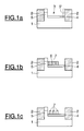
- the first step is to obtain a substrate comprising a body of monocrystalline silicon 1 and a lateral isolation 2 defining in the body a central part.
- lateral isolation generally defines a parallelepiped central part.
- This central part is provided with a recess 3, of generally parallelepiped shape having a horizontal bottom wall and vertical side walls.
- the bottom wall of the recess 3 is coated with a layer of oxide of silicon 4.
- a side wall of the recess 3 is defined by a monocrystalline silicon layer 5 however as the side wall opposite vertical can be formed by a wall of isolation lateral 2 or by a vertical layer 5 '(shown in dotted lines on FIG. 1a) similar to layer 5.
- the vertical layer 5 and possibly the vertical layer 5 ′ in monocrystalline silicon are generally coated on their upper surface with a thin layer silicon oxide.
- the other two opposite side walls of the recess are made of a dielectric material and preferably by a wall lateral isolation 2.
- the silicon / germanium alloys useful in the present invention are well known. Among these alloys, mention may be made of Si 1-X Ge X alloys where 0 ⁇ x ⁇ 1 and Si 1-xy Ge x C y alloys where 0 ⁇ x ⁇ 0.95 and 0 ⁇ y ⁇ 0.5. Preferably, for reasons of ease of selective etching, SiGe alloys having a relatively high germanium content will be chosen, preferably alloys for which x ⁇ 0.1, for example 0.1 ⁇ x ⁇ 0.3.
- the final step of the process consists of a selective etching of the SiGe alloy lines either by isotropic plasma etching or by etching using a well known oxidative chemistry.
- a selective etching solution such as a 40 ml HNO 3 70% + 1 ml H 2 O 2 + 5 ml HF 0.5% solution.
- the substrate described in FIG. 1a can be, as indicated previously obtained either from a silicon substrate classic solid monocrystalline, or a SOI substrate (silicon on insulator) classic.
- the silicon substrate classic solid monocrystalline includes a silicon body monocrystalline 1 and lateral isolation (STI) defining in this body a central part.
- STI lateral isolation
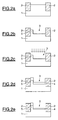
- FIG. 2b we start by forming conventional manner by means of a mask and by etching, a recess 3 in the central part of the monocrystalline silicon body 1 of so as to leave on a side wall of the insulation 2 delimiting the central part a part 5 of monocrystalline silicon. Wall opposite parallel side of the recess can be formed either directly as shown in Figure 2b by the lateral isolation 2 either by a silicon part similar to part 5.
- the bottom wall of the recess 3 is treated so as to modify this bottom wall in monocrystalline silicon and impart to it a higher oxidation rate than the vertical part 5 in monocrystalline silicon. constituting one of the side walls of the recess 3.
- This treatment can advantageously be a high dose implantation of an appropriate element or compound.
- suitable elements promoting the oxidation rate of monocrystalline silicon mention may be made of silicon, indium and arsenic.
- the compounds mention may be made of boron fluoride BF 2 . This implantation is carried out perpendicular to the bottom wall of the recess 3 so as to modify only the latter and not the vertical wall 5 of the recess.
- step 2c The structure obtained in step 2c is then subjected to a classic oxidation as shown in Figure 2d to form on the bottom wall and the side walls of the recess 3, a layer of silicon oxide 4. Due to the previous treatment, the layer thus formed is thicker on the bottom wall of the recess than on the side walls of the recess, in particular that on the wall in untreated monocrystalline silicon 5 and the opposite side wall of the recess. Obviously, the upper surface of the wall lateral 5 in monocrystalline silicon is also covered with a silicon oxide layer of thickness similar to that covering the bottom wall of the recess since this surface is also located treated during the previous treatment.
- the elimination is then carried out by etching, for example a conventional chemical etching of the silicon oxide layer covering the opposite side walls of the recess.
- etching for example a conventional chemical etching of the silicon oxide layer covering the opposite side walls of the recess.
- the etching step allows to expose the opposite side walls of the recess and in particular the wall constituted by part 5 in monocrystalline silicon while retaining on the bottom wall of the recess a layer of silicon oxide and thus obtaining the substrate as shown in FIG. 1a.
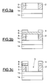
- the conventional SOI substrate includes a stack of a lower silicon layer monocrystalline 1a, of an intermediate layer of silicon oxide 1b and an upper layer constituted by a central part in monocrystalline silicon 1c delimited by lateral insulation 2.
- the mask 9 has a eccentric opening relative to the central part 1c so as to cover a portion of the central part in monocrystalline silicon 1c adjacent to a side wall of the insulation 2.
Landscapes
- Engineering & Computer Science (AREA)
- Chemical & Material Sciences (AREA)
- Nanotechnology (AREA)
- Physics & Mathematics (AREA)
- Mathematical Physics (AREA)
- Theoretical Computer Science (AREA)
- Crystallography & Structural Chemistry (AREA)
- Element Separation (AREA)
- Recrystallisation Techniques (AREA)
- Thin Film Transistor (AREA)
Abstract
Description
- un empilement d'une couche inférieure en silicium monocristallin, d'une couche intermédiaire d'oxyde de silicium et d'une couche supérieure comprenant une partie centrale en silicium monocristallin délimité par un isolement latéral;
- la formation sur la couche supérieure d'une couche mince d'oxyde de silicium;
- la formation sur la couche mince d'oxyde de silicium d'un masque;
- la gravure à travers le masque de la couche mince d'oxyde de silicium et de la partie centrale de la couche supérieure du substrat SOI avec arrêt sur la couche intermédiaire d'oxyde de silicium pour former un évidement ayant une paroi de fond en oxyde de silicium et une première paire de parois latérales parallèles opposées en matériau diélectrique et une deuxième paire de parois latérales parallèles opposées dont une au moins est constituée de silicium monocristallin; et
- l'élimination du masque.
Claims (14)
- Procédé de fabrication d'un réseau de lignes nanométriques en silicium monocristallin sur un substrat isolant caractérisé en ce qu'il comprend :(a) l'obtention d'un substrat comprenant un corps de silicium (1), un isolement latéral (2) définissant dans le corps (1) une partie centrale, un évidement (3) formé dans la partie centrale ayant une paroi de fond en matérieu diélectrique, de préférence SiO2, une première paire de parois latérales parallèles opposées en matériau diélectrique, de préférence SiO2, et une deuxième paire de parois latérales parallèles opposées, au moins une des parois latérales parallèles opposées de la deuxième paire étant constituée par du silicium monocristallin (5) ;(b) la croissance par épitaxie dans l'évidement (3), à partir de la paroi latérale en silicium monocristallin (5) de l'évidement, d'un réseau alterné de lignes parallèles en alliage SiGe monocristallin (6) et en silicium monocristallin (7) ; et(c) la gravure des lignes en alliage SiGe monocristallin (7), pour former dans l'évidement (3) un réseau de lignes parallèles en silicium monocristallin (7) isolées les unes des autres.
- Procédé selon la revendication 1, caractérisé en ce que les deux parois latérales parallèles opposées de la deuxième paire de parois latérales de l'évidement sont constituées par du silicium monocristallin (5, 5') et en ce que la croissance épitaxiale des lignes alternées (6, 7) s'effectue à partir des deux parois latérales parallèles opposées en silicium monocristallin.
- Procédé selon la revendication 1 ou 2, caractérisé en ce que les lignes alternées (6, 7) ont une largeur inférieure à 100 nm.
- Procédé selon la revendication 3, caractérisé en ce que les lignes alternées (6, 7) ont une largeur de 5 à 20nm.
- Procédé selon l'une quelconque des revendications précédentes, caractérisé en ce que l'obtention du substrat de l'étape (a) comprend :l'obtention d'un substrat massif en silicium monocristallin (1) comportant un isolement latéral (2) définissant une partie centrale du substrat massif ;le masquage et la gravure de la partie centrale pour y former un évidement (3) ayant une paroi de fond, une première paire de parois latérales parallèles opposées en matériau diélectrique et une deuxième paire de parois latérales parallèles opposées dont une au moins des parois est constituée par du silicium monocristallin (5) ;le traitement de la paroi de fond de l'évidement pour en accroítre la vitesse d'oxydation du silicium ;la formation sur la paroi de fond et les parois latérales parallèles opposées de la deuxième paire d'une couche d'oxyde de silicium (4) plus épaisse sur la paroi de fond que sur les parois latérales opposées; etla gravure isotrope de l'oxyde de silicium pour éliminer la couche d'oxyde de silicium des parois latérales parallèles opposées de la deuxième paire tout en laissant une couche d'oxyde de silicium sur la paroi de fond de l'évidement (3).
- Procédé selon la revendication 4, caractérisé en ce que l'étape de traitement de la paroi de fond comprend une implantation verticale d'une dose élevée d'un élément ou d'un composé accélérant l'oxydation du silicium monocristallin.
- Procédé selon la revendication 6, caractérisé en ce que les éléments sont choisis parmi Si, In et As et le composé est BF2.
- Procédé selon l'une quelconque des revendications 1 à 4, caractérisé en ce que l'obtention du substrat de l'étape (a) comprend :l'obtention d'un substrat dit SOI comprenant un empilement d'une couche inférieure en silicium monocristallin (1a), d'une couche intermédiaire d'oxyde de silicium (1b) et d'une couche supérieure comprenant une partie centrale en silicium monocristallin (1c) délimité par un isolement latéral (2) ;la formation sur la couche supérieure d'une couche mince d'oxyde de silicium (8) ;la formation sur la couche mince d'oxyde de silicium (8) d'un masque (9) ;la gravure à travers le masque (9) de la couche mince d'oxyde de silicium (8) et de la partie centrale (1c) de la couche supérieure du substrat SOI avec arrêt sur la couche intermédiaire d'oxyde de silicium (1b) pour former un évidement (3) ayant une paroi de fond en oxyde de silicium, une première paire de parois latérales parallèles opposées en matériau diélectrique et une deuxième paire de parois latérales parallèles opposées dont une au moins est constituée de silicium monocristallin (5) ; etl'élimination du masque (9).
- Dispositif comportant un substrat comprenant un corps de silicium monocristallin (1) et un isolement latéral (2) définissant dans le corps une partie centrale, caractérisé en ce que la partie centrale du corps (1) comporte un évidement (3) et dans cet évidement un réseau de lignes parallèles en silicium monocristallin (7) espacées et isolées entre elles.
- Dispositif selon la revendication 9, caractérisé en ce que l'évidement comporte une paroi de fond (4) en matériau diélectrique et que les lignes (7) du réseau reposent sur cette paroi de fond.
- Dispositif selon la revendication 10, caractérisé en ce que la paroi de fond (4) est en SiO2.
- Dispositif selon l'une quelconque des revendications 9 à 11, caractérisé en ce que le réseau de lignes (7) est enterré.
- Dispositif selon l'une quelconque des revendications 9 à 12, caractérisé en ce que les lignes (7) du réseau sont isolées entre elles par un matériau diélectrique gazeux ou solide.
- Dispositif selon l'une quelconque des revendications 9 à 13, caractérisé en ce que les lignes (7) en silicium monocristallin ont une largeur de 5 à 20 nm.
Applications Claiming Priority (2)
| Application Number | Priority Date | Filing Date | Title |
|---|---|---|---|
| FR9915902A FR2802705B1 (fr) | 1999-12-16 | 1999-12-16 | Procede de fabrication d'un reseau de lignes nanometriques en silicium monocristallin et dispositif obtenu |
| FR9915902 | 1999-12-16 |
Publications (1)
| Publication Number | Publication Date |
|---|---|
| EP1109209A1 true EP1109209A1 (fr) | 2001-06-20 |
Family
ID=9553353
Family Applications (1)
| Application Number | Title | Priority Date | Filing Date |
|---|---|---|---|
| EP00403511A Withdrawn EP1109209A1 (fr) | 1999-12-16 | 2000-12-14 | Procédé de fabrication d'un réseau de lignes nanométriques en silicium monocristallin et dispositif obtenu |
Country Status (3)
| Country | Link |
|---|---|
| US (1) | US6583451B2 (fr) |
| EP (1) | EP1109209A1 (fr) |
| FR (1) | FR2802705B1 (fr) |
Families Citing this family (4)
| Publication number | Priority date | Publication date | Assignee | Title |
|---|---|---|---|---|
| JP3890254B2 (ja) * | 2002-05-07 | 2007-03-07 | 沖電気工業株式会社 | 半導体装置の製造方法 |
| CN1314958C (zh) * | 2004-06-10 | 2007-05-09 | 上海交通大学 | 含水多孔介质材料的传热性质和孔隙流动性质的测试装置 |
| US9748259B1 (en) * | 2016-02-25 | 2017-08-29 | Globalfoundries Inc. | Method of forming a semiconductor device structure and semiconductor device structure |
| US20250239450A1 (en) * | 2024-01-24 | 2025-07-24 | Globalfoundries U.S. Inc. | Structures including a semiconductor layer formed by lateral epitaxial growth |
Citations (6)
| Publication number | Priority date | Publication date | Assignee | Title |
|---|---|---|---|---|
| JPS5941840A (ja) * | 1982-09-01 | 1984-03-08 | Nippon Telegr & Teleph Corp <Ntt> | 微細パタ−ン形成方法 |
| EP0661733A2 (fr) * | 1993-12-21 | 1995-07-05 | International Business Machines Corporation | Dispositifs de fil quantique mono-dimensionnel en silicium et méthode de fabrication |
| FR2741195A1 (fr) * | 1995-11-10 | 1997-05-16 | Thomson Csf | Dispositif a puits quantique et procede de realisation |
| US5630905A (en) * | 1995-02-06 | 1997-05-20 | The Regents Of The University Of California | Method of fabricating quantum bridges by selective etching of superlattice structures |
| US5705321A (en) * | 1993-09-30 | 1998-01-06 | The University Of New Mexico | Method for manufacture of quantum sized periodic structures in Si materials |
| EP0951055A2 (fr) * | 1998-04-17 | 1999-10-20 | Hewlett-Packard Company | Couche formée par croissance epitaxiale dans une tranchée |
Family Cites Families (7)
| Publication number | Priority date | Publication date | Assignee | Title |
|---|---|---|---|---|
| JP2757258B2 (ja) * | 1988-11-01 | 1998-05-25 | 日本電信電話株式会社 | 超格子素子の製造方法 |
| US4987094A (en) * | 1989-06-02 | 1991-01-22 | Bell Communications Research, Inc. | Method of making a macroscopic stepped structure on a vicinally cut crystal |
| FR2667617B1 (fr) * | 1990-10-09 | 1992-11-27 | Thomson Csf | Procede de croissance de couches heteroepitaxiales. |
| US5212110A (en) * | 1992-05-26 | 1993-05-18 | Motorola, Inc. | Method for forming isolation regions in a semiconductor device |
| TW241372B (fr) * | 1993-04-07 | 1995-02-21 | Hitachi Seisakusyo Kk | |
| US5962863A (en) * | 1993-09-09 | 1999-10-05 | The United States Of America As Represented By The Secretary Of The Navy | Laterally disposed nanostructures of silicon on an insulating substrate |
| US6110278A (en) * | 1998-08-10 | 2000-08-29 | Saxena; Arjun N. | Methods for and products of growth of single-crystal on arrayed nucleation sites (SCANS) defined in nucleation unfriendly substrates |
-
1999
- 1999-12-16 FR FR9915902A patent/FR2802705B1/fr not_active Expired - Fee Related
-
2000
- 2000-12-14 EP EP00403511A patent/EP1109209A1/fr not_active Withdrawn
- 2000-12-15 US US09/738,870 patent/US6583451B2/en not_active Expired - Lifetime
Patent Citations (6)
| Publication number | Priority date | Publication date | Assignee | Title |
|---|---|---|---|---|
| JPS5941840A (ja) * | 1982-09-01 | 1984-03-08 | Nippon Telegr & Teleph Corp <Ntt> | 微細パタ−ン形成方法 |
| US5705321A (en) * | 1993-09-30 | 1998-01-06 | The University Of New Mexico | Method for manufacture of quantum sized periodic structures in Si materials |
| EP0661733A2 (fr) * | 1993-12-21 | 1995-07-05 | International Business Machines Corporation | Dispositifs de fil quantique mono-dimensionnel en silicium et méthode de fabrication |
| US5630905A (en) * | 1995-02-06 | 1997-05-20 | The Regents Of The University Of California | Method of fabricating quantum bridges by selective etching of superlattice structures |
| FR2741195A1 (fr) * | 1995-11-10 | 1997-05-16 | Thomson Csf | Dispositif a puits quantique et procede de realisation |
| EP0951055A2 (fr) * | 1998-04-17 | 1999-10-20 | Hewlett-Packard Company | Couche formée par croissance epitaxiale dans une tranchée |
Non-Patent Citations (2)
| Title |
|---|
| JURCZAK M ET AL: "INVESTIGATION ON THE SUITABILITY OF VERTICAL MOSFET'S FOR HIGH SPEED (RF) CMOS APPLICATIONS", PROCEEDINGS OF THE EUROPEAN SOLID STATE DEVICE RESEARCH CONFERENCE (ESSDERC), 1998, XP000949963 * |
| PATENT ABSTRACTS OF JAPAN vol. 008, no. 131 (E - 251) 19 June 1984 (1984-06-19) * |
Also Published As
| Publication number | Publication date |
|---|---|
| US20010005618A1 (en) | 2001-06-28 |
| US6583451B2 (en) | 2003-06-24 |
| FR2802705B1 (fr) | 2002-08-09 |
| FR2802705A1 (fr) | 2001-06-22 |
Similar Documents
| Publication | Publication Date | Title |
|---|---|---|
| EP1837916A1 (fr) | Procédé de réalisation d'un transistor à canal comprenant du germanium | |
| EP1918744B1 (fr) | Procédé de réalisation d'un guide a fente | |
| EP2654083A1 (fr) | Procédé ameliore de réalisation d'une structure de transistor a nano-fils superposes et a grille enrobante | |
| EP1869712B1 (fr) | Structure et procede de realisation d'un dispositif microelectronique dote d'un ou plusieurs fils quantiques aptes a former un canal ou plusieurs canaux de transistors | |
| EP3502049B1 (fr) | Procede de realisation d'un dispositif semi-conducteur comprenant une ou plusieurs nanostructures | |
| WO2006131615A1 (fr) | Transistor a canal a base de germanium enrobe par une electrode de grille et procede de fabrication d'un tel transistor | |
| JP5008786B2 (ja) | プレーナ・ヘテロ構造の製造方法 | |
| FR3100377A1 (fr) | Prise de contact sur du germanium | |
| EP1139407A1 (fr) | Procédé de fabrication d'un transistor bipolaire de type double-polysilicium auto-aligné à base à hétérojonction et transistor correspondant | |
| EP1589572B1 (fr) | Procédé de fabrication d'un circuit intégré comprenant l'élaboration de tranchées d'isolation creuses | |
| EP1132955A1 (fr) | Procédé de fabrication d'un transistor bipolaire double-polysilicium autoaligné. | |
| FR2717306A1 (fr) | Procédé d'isolement de zones actives d'un substrat semi-conducteur par tranchées peu profondes, notamment étroites, et dispositif correspondant. | |
| FR2802705A1 (fr) | Procede de fabrication d'un reseau de lignes nanometriques en silicium monocristallin et dispositif obtenu | |
| FR2799307A1 (fr) | Dispositif semi-conducteur combinant les avantages des architectures massives et soi, procede de fabrication | |
| FR3023058A1 (fr) | Procede de realisation d'un dispositif microelectronique | |
| FR2718287A1 (fr) | Procédé de fabrication d'un transistor à effet de champ à grille isolée, en particulier de longueur de canal réduite, et transistor correspondant. | |
| EP3809450A1 (fr) | Procede d'hetero-integration d'un materiau semi-conducteur d'interet sur un substrat de silicium | |
| FR2564241A1 (fr) | Procede de fabrication de circuits integres du type silicium sur isolant | |
| US10553741B2 (en) | Method for producing a photodiode and photodiode | |
| EP3968388B1 (fr) | Procédé de fabrication d'une zone dopée d'un dispositif microélectronique | |
| EP1836526A1 (fr) | Modulateur a jonction capacitive, jonction capacitive et son procede de realisation | |
| FR2921754A1 (fr) | Procede de fabrication d'un subtrat semiconducteur localise sur une couche isolante | |
| FR2790867A1 (fr) | Procede de fabrication de transistor bipolaire | |
| FR2889622A1 (fr) | Procede de fabrication d'un transistor a nanodoigts semiconducteurs paralleles | |
| FR3157661A1 (fr) | Procédé de réalisation d’un dispositif microélectronique sur substrat fd-soi, dispositif correspondant et circuit intégré l’incorporant |
Legal Events
| Date | Code | Title | Description |
|---|---|---|---|
| PUAI | Public reference made under article 153(3) epc to a published international application that has entered the european phase |
Free format text: ORIGINAL CODE: 0009012 |
|
| AK | Designated contracting states |
Kind code of ref document: A1 Designated state(s): DE FR GB IT |
|
| AX | Request for extension of the european patent |
Free format text: AL;LT;LV;MK;RO;SI |
|
| RAP1 | Party data changed (applicant data changed or rights of an application transferred) |
Owner name: FRANCE TELECOM Owner name: STMICROELECTRONICS S.A. |
|
| 17P | Request for examination filed |
Effective date: 20011210 |
|
| AKX | Designation fees paid |
Free format text: DE FR GB IT |
|
| STAA | Information on the status of an ep patent application or granted ep patent |
Free format text: STATUS: THE APPLICATION IS DEEMED TO BE WITHDRAWN |
|
| 18D | Application deemed to be withdrawn |
Effective date: 20090701 |