EP0951055A2 - Couche formée par croissance epitaxiale dans une tranchée - Google Patents
Couche formée par croissance epitaxiale dans une tranchée Download PDFInfo
- Publication number
- EP0951055A2 EP0951055A2 EP98121119A EP98121119A EP0951055A2 EP 0951055 A2 EP0951055 A2 EP 0951055A2 EP 98121119 A EP98121119 A EP 98121119A EP 98121119 A EP98121119 A EP 98121119A EP 0951055 A2 EP0951055 A2 EP 0951055A2
- Authority
- EP
- European Patent Office
- Prior art keywords
- trench
- layer
- growth
- epitaxial
- dislocation density
- Prior art date
- Legal status (The legal status is an assumption and is not a legal conclusion. Google has not performed a legal analysis and makes no representation as to the accuracy of the status listed.)
- Withdrawn
Links
Images


Classifications
-
- H—ELECTRICITY
- H10—SEMICONDUCTOR DEVICES; ELECTRIC SOLID-STATE DEVICES NOT OTHERWISE PROVIDED FOR
- H10P—GENERIC PROCESSES OR APPARATUS FOR THE MANUFACTURE OR TREATMENT OF DEVICES COVERED BY CLASS H10
- H10P14/00—Formation of materials, e.g. in the shape of layers or pillars
- H10P14/20—Formation of materials, e.g. in the shape of layers or pillars of semiconductor materials
- H10P14/27—Formation of materials, e.g. in the shape of layers or pillars of semiconductor materials using selective deposition, e.g. simultaneous growth of monocrystalline and non-monocrystalline semiconductor materials
- H10P14/276—Lateral overgrowth
-
- H—ELECTRICITY
- H10—SEMICONDUCTOR DEVICES; ELECTRIC SOLID-STATE DEVICES NOT OTHERWISE PROVIDED FOR
- H10P—GENERIC PROCESSES OR APPARATUS FOR THE MANUFACTURE OR TREATMENT OF DEVICES COVERED BY CLASS H10
- H10P14/00—Formation of materials, e.g. in the shape of layers or pillars
- H10P14/20—Formation of materials, e.g. in the shape of layers or pillars of semiconductor materials
- H10P14/27—Formation of materials, e.g. in the shape of layers or pillars of semiconductor materials using selective deposition, e.g. simultaneous growth of monocrystalline and non-monocrystalline semiconductor materials
- H10P14/271—Formation of materials, e.g. in the shape of layers or pillars of semiconductor materials using selective deposition, e.g. simultaneous growth of monocrystalline and non-monocrystalline semiconductor materials characterised by the preparation of substrate for selective deposition
- H10P14/272—Formation of materials, e.g. in the shape of layers or pillars of semiconductor materials using selective deposition, e.g. simultaneous growth of monocrystalline and non-monocrystalline semiconductor materials characterised by the preparation of substrate for selective deposition using mask materials other than SiO2 or SiN
-
- H—ELECTRICITY
- H10—SEMICONDUCTOR DEVICES; ELECTRIC SOLID-STATE DEVICES NOT OTHERWISE PROVIDED FOR
- H10P—GENERIC PROCESSES OR APPARATUS FOR THE MANUFACTURE OR TREATMENT OF DEVICES COVERED BY CLASS H10
- H10P14/00—Formation of materials, e.g. in the shape of layers or pillars
- H10P14/20—Formation of materials, e.g. in the shape of layers or pillars of semiconductor materials
- H10P14/29—Formation of materials, e.g. in the shape of layers or pillars of semiconductor materials characterised by the substrates
- H10P14/2901—Materials
-
- H—ELECTRICITY
- H10—SEMICONDUCTOR DEVICES; ELECTRIC SOLID-STATE DEVICES NOT OTHERWISE PROVIDED FOR
- H10P—GENERIC PROCESSES OR APPARATUS FOR THE MANUFACTURE OR TREATMENT OF DEVICES COVERED BY CLASS H10
- H10P14/00—Formation of materials, e.g. in the shape of layers or pillars
- H10P14/20—Formation of materials, e.g. in the shape of layers or pillars of semiconductor materials
- H10P14/29—Formation of materials, e.g. in the shape of layers or pillars of semiconductor materials characterised by the substrates
- H10P14/2901—Materials
- H10P14/2921—Materials being crystalline insulating materials
-
- H—ELECTRICITY
- H10—SEMICONDUCTOR DEVICES; ELECTRIC SOLID-STATE DEVICES NOT OTHERWISE PROVIDED FOR
- H10P—GENERIC PROCESSES OR APPARATUS FOR THE MANUFACTURE OR TREATMENT OF DEVICES COVERED BY CLASS H10
- H10P14/00—Formation of materials, e.g. in the shape of layers or pillars
- H10P14/20—Formation of materials, e.g. in the shape of layers or pillars of semiconductor materials
- H10P14/34—Deposited materials, e.g. layers
- H10P14/3402—Deposited materials, e.g. layers characterised by the chemical composition
- H10P14/3414—Deposited materials, e.g. layers characterised by the chemical composition being group IIIA-VIA materials
- H10P14/3416—Nitrides
Definitions
- the present invention relates generally to the fabrication of semiconductor materials, and, more particularly, to a new fabrication configuration having an epitaxial material grown laterally in a trench and a method for producing same.
- a building block of many electronic devices such as diodes, transistors, and lasers is the p-n junction.
- the p-n junction, or active region is typically formed from epitaxial growth material, which is in turn grown on a substrate.
- the growth material can be referred to as semiconductor material.
- the semiconductor material is typically fabricated by growing an epitaxial layer of a chosen material upon a substrate material.
- the substrate material may be, and frequently is, of a different composition than the material used to grow the epitaxial layer.
- the epitaxial layer is typically a thin single crystalline film that is deposited upon a crystalline substrate.
- the epitaxial layer is typically deposited so that the crystal lattice structure of the epitaxial layer closely matches the crystal lattice structure of the substrate.
- a large number of defects, or dislocations can result.
- Dislocations manifest in the form of imperfections in the crystal structure and can result in high optical loss, low optical efficiency, non uniform quantum wells in the active region, or the reduction of the electrical quality of the material, thus preventing the material from being used to fabricate certain devices, such as lasers and transistor structures.
- a largely dislocation-free material is desired for these highly critical devices.
- Dislocations are typical when trying to grow an epitaxial layer over a substrate having a different lattice structure. Dislocation densities on the order of 10 7 to 10 9 dislocations per square centimeter (cm 2 ) can be common and result in poor semiconductor material that is unusable for certain critical applications.
- Dislocation density can be reduced by adding a mask layer over the substrate material prior to growing the epitaxial layer. When the epitaxial layer is then grown over the mask, the epitaxial layer grows laterally, resulting in a reduced dislocation density being present in the portion of the epitaxial layer that resides over the mask. Because the dislocations tend to propagate vertically, the vertically grown material present m the unmasked region of a wafer will be of higher dislocation density as the defects will continue to propagate throughout the layer.
- multiple layers of making material having multiple layers of epitaxial growth may further reduce the dislocation density. While the growing of multiple epitaxial layers over mask layers has some benefit, a drawback is that the mask layer adds cost, complexity and can add contamination to the epitaxial growth material. Successive iterations may yield low dislocation density material over the entire wafer. It would be desirable to grow the material in a manner in which the low dislocation density material is present over the entire wafer in a single growth sequence.
- the invention provides an epitaxial material grown laterally in a trench and a method for producing same. Although not limited to these particular applications, the material and method for producing it are particularly suited for fabrication of high quality GaN material system epitaxial layers over a sapphire substrate.
- the GaN material system can include members of the Group III-V family including, but not limited to, gallium nitride (GaN), indium gallium nitride (InGaN), indium nitride (InN), aluminum gallium nitride (AlGaN), aluminum nitride (AlN), aluminum indium gallium nitride (AlInGaN), gallium arsenide nitride (GaAsN), indium gallium arsenide nitride (InGaAsN), aluminum gallium arsenide nitride (AlGaAsN), gallium phosphide nitride (GaPN), indium gallium phosphi
- the present invention can be conceptualized as providing a method for growing a low dislocation density material comprising the following steps. First, a trench is formed in a substrate. Alternatively, an epitaxial layer is grown over a substrate and a trench is formed therein. The trench is formed preferably by etching the substrate or the first epitaxial layer. An epitaxial lateral growth layer is then grown in the trench, the growth layer originating from the side walls of the trench. Illustratively the epitaxial lateral growth layer can partially fill, completely fill, or overflow the trench. It is also possible to apply a mask layer, which can be either an insulating layer or a conducting layer, at the bottom of the trench, over the top of the first epitaxial layer, or any combination thereof.
- a mask layer which can be either an insulating layer or a conducting layer, at the bottom of the trench, over the top of the first epitaxial layer, or any combination thereof.
- the epitaxial lateral growth layer can be grown from a single wall of the trench laterally across the trench, and eventually filling and overflowing the trench.
- a device having a p-n junction, or active region can be grown in the epitaxial lateral growth layer.
- the aforementioned method for multiple lateral growth of an epitaxial layer including the forming of a trench in the epitaxial material results in a low dislocation density material as follows.
- a low dislocation density material system comprises a substrate, or alternatively, a first epitaxial layer over a substrate.
- a trench is formed, preferably by etching, in the substrate or the first epitaxial layer.
- An epitaxial lateral growth layer is then grown in the trench, the growth layer extending from the side walls of the trench.
- the material can further comprise a mask layer, the mask layer being either insulating material or conducting material and applied to the bottom of the trench, over the first epitaxial layer, or any combination thereof.
- the mask material is designed to further control and define the growth pattern of the epitaxial lateral growth layer.
- one side wall of the trench can be coated with the mask layer, and the epitaxial lateral growth layer can then be grown from the opposing side wall of the trench.
- the epitaxial lateral growth layer can have a p-n junction, or active region, formed therein.
- the invention has numerous advantages, a few which are delineated, hereafter, as merely examples.
- An advantage of the invention is that it increases the yield of high quality, low dislocation density material in an epitaxial layer grown over a substrate.
- Another advantage of the invention is that it reduces the amount of optical loss in the epitaxial layer of a semiconductor material.
- Another advantage of the invention is that it increases the optical efficiency in the epitaxial layer of a semiconductor material.
- Another advantage of the invention is that it improves the electrical performance of the material forming the epitaxial layer of a semiconductor.
- Another advantage of the invention is that contamination arising from the use of a mask can be reduced or eliminated.
- Another advantage of the invention is that it is simple in design and easily implemented on a mass scale for commercial production.
- the present invention can be implemented using a variety of substrate and epitaxial growth materials. While applicable to a variety of materials where the defects tend to propagate along a particular growth direction, the preferred embodiment of the low dislocation density method and material is particularly useful for growing a gallium nitride (GaN) material system epitaxial layer over a sapphire substrate.
- GaN gallium nitride
- the GaN material system can include members of the Group III-V family including, but not limited to, gallium nitride (GaN), indium gallium nitride (InGaN), indium nitride (InN), aluminum gallium nitride (AlGaN), aluminum nitride (AlN), aluminum gallium nitride (AlGaN), aluminum indium gallium nitride (AlInGaN), gallium arsenide nitride (GaAsN), indium gallium arsenide nitride (InGaAsN), aluminum gallium arsenide nitride (AlGaAsN), gallium phosphide nitride (GaPN), indium gallium phosphide nitride (InGaPN), aluminum gallium phosphide nitride (AlGaPN), etc .
- the concepts and features of the present invention are applicable to other epi
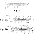
- Fig. 1 shown is a schematic cross-sectional view of a typical GaN epitaxial layer 10 grown on a sapphire substrate 17.
- the high density of dislocations 18 in the GaN epitaxial layer 10 is a result of a large lattice mismatch between the epitaxial layer 10 and the substrate 17.
- the dislocations 18 run predominantly vertically through the epitaxial layer along the growth direction.
- the growth direction is vertical.
- lattice planes 12 which cut horizontally across the surface expose every dislocation and hence contain the maximum dislocation density per unit area.
- lattice planes 19 running vertically from the substrate up to the surface intersect far fewer dislocations since these lattice planes run substantially parallel to the dislocations and hence, contain the minimum dislocations per unit area of any lattice plane.
- an exposed vertical, or nearly vertical, sidewall of the original epitaxial layer has a dramatically reduced density of dislocations and hence serves as an excellent surface from which to grow additional GaN material. This concept forms the basis for the invention described herein.
- an epitaxial layer contains dislocations which run substantially along a particular direction in the crystal, then regrowing additional epitaxial material in a direction which lies perpendicular to the predominant direction of dislocations can dramatically reduce the density of dislocations in the regrown layer.
- any type of regrowth directed along the horizontal or lateral direction should improve the material quality of the regrown layer.
- rotating the growth direction by 90 degrees reduces the density of dislocations and produces higher quality material.
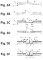
- Figs. 2A and 2B shown is an existing method of rotating the growth direction.
- the GaN 20 which grows up from the unmasked areas around the SiO 2 stripes is forced to grow laterally in order to cover the SiO 2 .
- This laterally grown layer 21 therefore accomplishes the desired 90 degree growth rotation and as a result has fewer dislocations than the original layer 10. Additional growth will force the growth direction vertical again above layer 21 forming epitaxial layer 22.
- the final surface of the wafer will therefore be covered with a mixture of epitaxial layers 22, which have gone through two (2) growth rotations and hence should be of high quality (low dislocation density), and epitaxial layers 20 which have grown up vertically from the substrate and have gone through zero (0) growth rotations.
- Epitaxial layers 20 propagate the original dislocations, and hence are of low quality (high dislocation density).
- the number of growth rotations occurring before a given layer is regrown is indicated for each layer in Fig. 2 and the figures hereinafter. It should also be pointed out that where the growth fronts of layers 21 meet in the center of the SiO 2 stripe 14, a dislocation 16, or possibly a void, is formed.
- a void can be an area below the dislocation formed where the growth fronts do not completely meet.
- Some of the disadvantages of the existing method for rotating the growth direction are that portions of the final surface still contain low quality, high dislocation density material 20.
- the dislocation and/or void 16 in the center of the SiO 2 stripe may also be undesirable.
- the SiO 2 mask itself is a source of oxygen contamination in the epitaxial growth process and can degrade the quality of the regrown layers.
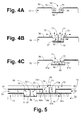
- Figs. 3A through 3F shown are schematic views illustrating the growth progression of the low dislocation density material of the present invention.
- the present invention allows for the growth of high quality, low dislocation density epitaxial material across the entire surface of a wafer in a single regrowth step. This is accomplished by initiating the growth on the sidewalls of a trench or array of trenches formed in a GaN epitaxial layer or substrate material. Additionally, maskless regrowth under certain growth conditions (those which favor lateral growth over vertical growth) is possible with the present invention, which eliminates the possibility of growth contamination originating from a mask layer.
- first epitaxial layer 70 is grown on sapphire substrate layer 52.
- Layer 52 can be other substrate material as known in the art, including but not limited to, silicon (Si), gallium arsenide (GaAs), silicon carbide (SiC), or indium phosphide (InP). While illustratively GaN in the preferred embodiment, first epitaxial layer 70 may be various other materials including, but not limited to, any of the GaN material system.
- the GaN material system can include members of the Group III-V family including, but not limited to, gallium nitride (GaN), indium gallium nitride (InGaN), indium nitride (InN), aluminum Gallium nitride (AlGaN), aluminum nitride (AlN), aluminum gallium nitride (AlGaN), aluminum indium gallium nitride (AlInGaN), gallium arsenide nitride (GaAsN), indium gallium arsenide nitride (InGaAsN), aluminum gallium arsenide nitride (AlGaAsN), gallium phosphide nitride (GaPN), indium gallium phosphide nitride (InGaPN), aluminum gallium phosphide nitride (AlGaPN), etc . Also shown in first epitaxial layer 70 are dislocations 54.
- trench 60 can be formed, preferably by etching, in first epitaxial layer 70.
- Trench 60 is depicted as extending down to substrate 52, however trench 60 need not extend completely to substrate 52.
- Trench 60 has substantially vertical sidewalls 61a and 61b. However, it is important to note that while trench 60 is shown in the preferred embodiment having substantially vertical sidewalls, it is possible for trench 60 to have sloped side walls as well.
- epitaxial lateral growth 71 which originates from the sidewalls 61a and 61b of trench 60 will be of much higher quality than the original layer 70 because the lateral growth is starting from a lattice template or plane which cuts through the fewest possible dislocations of the original epitaxial layer 70.
- regrown layer 71 since regrown layer 71 has gone through one (1) growth rotation, it should be of higher quality with fewer dislocations than the original layer 70.
- mask layer 56 could be, depending upon the material characteristics desired, either an insulator like SiO 2 or a conducting material like tungsten.
- Mask layer 56 can cover the horizontal surfaces of substrate 52, or first epitaxial layer 70, or any combination thereof so that the vertical growth of the epitaxial lateral growth layer 71 can be further suppressed.
- the growth conditions are such that the lateral growth rate is much faster than the vertical growth rate, mask 56 may not be necessary at all.
- the omission of a mask for the regrowth step is desirable for minimizing contamination in the growth process and hence is an important potential benefit of the present invention.
- a dislocation 57 or possibly a void, is formed. From this point, the material comprising epitaxial lateral growth layer 71 proceeds to grow vertically again, representing another growth rotation. Epitaxial layer 72 therefore has gone through two (2) growth rotations as indicated in Fig. 3E. Finally, another growth rotation occurs as layer 73 is grown laterally out from layer 72, spilling out on top of first epitaxial layer 70. The final surface of the wafer will therefore eventually be covered with a mixture of epitaxial layers 73 and 72 which have both gone through at least two (2) growth rotations, and hence should both be of significantly higher quality than first epitaxial layer 70.
- the present invention using the same number of regrowth steps, provides not only complete wafer coverage with high quality material, but also produces some surface layers which have gone through more growth rotations and hence are potentially higher in quality than layers created with the existing method of Figs. 2A and 2B.
- the above description of growth inside and over a trench is illustrative in that the layer growth does not necessarily proceed in such an orderly time sequence from layer 71 to 72 to 73, etc .
- layer 72 will start growing before the growth fronts of layer 71 meet each other.
- the boundaries between layers having different numbers of growth rotations are not as well-defined or as rectangular as indicated in Figs. 3D, 3E and 3F.
- the above simplified description serves to illustrate the basic growth sequence and how the material quality potentially improves as it grows out of the trench and goes through a complete 180 degree change in growth direction, eventually covering the entire surface of the wafer, or substrate.
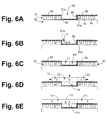
- Fig. 4A shown is the substrate material of Figs. 3A through 3F having a trench 60 formed therein.
- Substrate 52 has trench 60 formed therein similarly to that described with respect to Fig. 3C.
- Optional mask layer 56 can be applied to the base of trench 60, to the horizontal surfaces of substrate 52, or to a combination thereof such that vertical growth can be further suppressed.
- the lateral growth of first epitaxial layer 70 from the sidewalls in this example produces GaN much like the quality shown in Fig. 1.
- Fig. 4C illustrates that if, for example, a cubic zinc-blende structure such as silicon is used as the substrate 52, a trench 60 having non-vertical sidewalls 61a and 61b can be etched in substrate 52. The non-vertical sidewalls 61a and 61b will direct the dislocations 54 downward trapping them more effectively in the trench 60, while the vertical growth 71 proceeds largely free of the original dislocations generated in layer 70.
- a cubic zinc-blende structure such as silicon
- FIG. 5 shown are multiple lateral growth layers of the low dislocation density material of Figs. 3A through 3F.
- Fig. 5 illustrates that the trench growth procedure can be used iteratively to potentially further improve the material quality.
- an additional trench 65 could be formed in layer 73 and mask 56, if desired, can be redeposited.
- the 180 degree change in growth direction again wraps around optional mask layer 56 on the surface of layer 73 and produces layer 73b growing laterally inward from the sidewalls 62a and 62b of additional trench 65 of layer 73.
- layer 74 then grows vertically over layer 73b, and layer 75 grows laterally outward again from layer 74.
- the upper layers 75 and 74 which cover the surface, have gone through five (5) and four (4) growth rotations respectively, again with a dislocation 57b at the center of the trench.
- two additional growth rotations are possible with each iteration.
- Figs. 6A through 6E shown are schematic views illustrating an alternate embodiment of the growth of the low dislocation density material of Figs. 3A through 3F. It is possible to eliminate dislocation 57 by growing epitaxial lateral growth material from only one sidewall, 61a for example, of trench 60. Either sidewall 61a or 61b may be used to originate the epitaxial lateral growth layer, sidewall 61a being used in this preferred embodiment for illustration. This is accomplished by masking opposing sidewall 61b as shown in Fig. 6B. Epitaxial lateral growth 71 is initiated from sidewall 61a and growth proceeds across trench 60, in this case filling and then spilling out over the top of the trench 60. As described above with respect to Figs. 3A through 3F, layers 71-73 are produced covering the entire surface of the substrate, or wafer, with high quality, low dislocation density epitaxial material; however, dislocation 57 is eliminated.
- epitaxial lateral growth layer 71 completely filing trench 60. While shown as growing laterally, epitaxial lateral growth layer 71 has both a lateral growth rate and a vertical growth rate, however, for simplicity, is shown as primarily growing laterally.
- Fig. 6D shown is epitaxial lateral growth layer 72 growing out of trench 60 and over first epitaxial lateral growth layer 71.
- Fig. 6E shows all epitaxial lateral growth layer 73 growing laterally and forming a very low dislocation material of epitaxial growth.
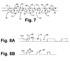
- Fig. 7 shown is an array of the trenches of Figs. 3A-3F, Figs. 4A-4C, Fig. 5, and Figs. 6A-6E covering an entire substrate, or wafer. It is possible to cover an entire wafer with the low dislocation density material described herein by forming arrays of trenches as shown in Fig. 7.
- This extension to the single trench concept can be applied to all methods and materials discussed above.
- the single sidewall trench method and material illustrated in Figs. 6A through 6E can be extended to arrays of trenches 60 as shown in Fig. 7.
- epitaxial lateral growth layers 73 meet each other between trenches 60 and form dislocations 57.
- Figs. 8A and 8B shown are trenches 60 and mesas 90 that can be etched or formed in an epitaxial layer and used to develop the low dislocation density material of Figs. 3A-3F, Figs. 4A-4C, Fig. 5, and Figs. 6A-6E.
- Mesas 90 are equally valid structures for initiating sidewall growth on sidewalls 91a and 91b. In this arrangement it may be useful to minimize horizontal section 90 to obtain as much lateral growth as possible between mesas, in effect using the mesas as thin vertical seeds for lateral growth.
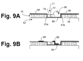
- Figs. 9A and 9B shown are schematic views illustrating an active region formed in the low dislocation density material of Figs. 3A-3F and Figs. 6A-6E.
- active regions which, for example, may include p-n junctions for light emitters, quantum wells, or even transistor structures directly on the sidewalls. Growing active regions in this manner results in devices capable of improved performance.
- first epitaxial layer 70 Upon substrate 52, which is illustratively sapphire, is grown first epitaxial layer 70.
- Trench 60 is formed into first epitaxial layer 70 similarly to that described with respect to Figs. 3A-3F and 6A-6E.
- optional mask layer 56 which can be either a conducting material or insulating material can be applied to the base of trench 60.
- Optional mask layer 56 can also be applied to the top horizontal surfaces of first epitaxial layer 70, and to wall 61b of trench 60.
- first epitaxial layer 70 can be of an n-type material.
- First epitaxial layer 70 can illustratively be either n-type or p-type material depending upon the characteristics of the device being fabricated.
- epitaxial lateral growth layer 71 is grown from side wall 61a using n-type material 78.
- Epitaxial lateral growth layer 71 begins with n-type material section 78 and is followed by active region 77, which is followed by p-type material 79.
- epitaxial lateral growth layer 71 comprises a device having a p-n junction.
- Active region 77 can be for example, but not limited to a quantum well active region of indium gallium nitride (InGaN) in a p-n junction for an optical device such as a light emitting diode (LED) or laser; or it can be a transistor.
- InGaN indium gallium nitride
- Fig. 9B shown is epitaxial lateral growth layer 71 having p-ohmic contact material 86 applied thereto. Similarly, if applied, mask layer 56 is removed from first epitaxial layer 70 so that n-ohmic contact material 84 can be applied directly thereto.
- the foregoing illustrates a p-n junction having electrical contacts 84 and 86 applied thereto, thus illustrating the formation of a high quality optical device using the concepts and features of the low dislocation density method and material of the present invention.
- Fig. 10 shown is a schematic detail view of the low dislocation density material of Figs. 3A-3F, Figs. 4A-4C, Fig. 5, and Figs. 6A-6E.
- Layer 71 which grows laterally out from the sidewall 61a, may not be entirely dislocation-free. Some of the vertical dislocations 54 in layer 70, which intersect the sidewall growth plane will turn sideways and continue to propagate into layer 71, illustrated as dislocations 58a.
- the density of dislocations 58a should be substantially lower than those present in layer 70.
- a plane is cut across substantially parallel to the dislocations 58a in layer 71, which implies that the lattice template for growth of layer 72 should contain only a small fraction of the lateral dislocations 58a in layer 71. The result is that even fewer dislocations 58b will propagate vertically into layer 72.
- the density of dislocations 58c propagating laterally in layer 73 should be much lower than those propagating vertically in layer 72. In this way, successive growth rotations can successively reduce the dislocation density, enabling the iterative procedure illustrated with respect to Fig. 5 the potential for producing very high quality material.
- FIGs. 11A-11C shown is an alternative embodiment of the additional trench of Fig. 5.
- FIGs. 10 and 11A shown, from a top view, is an additional mode of dislocation propagation which may not benefit from the dislocation density reduction procedure described with reference to Fig. 10.
- first epitaxial layer 70 is actually comprised of columns of single crystal domains 100 in which boundary surfaces 101 separating the domains contain vertical threads of edge dislocations 54. When a vertical side wall 61a is exposed, these boundary surfaces terminate along the interface formed by substantially vertical sidewall 61a. Regrowing on the sidewall will then propagate these planes 106 containing threads of vertical dislocations 54 in the growth direction to form layer 71.
- the resulting layer 71 comprises slabs of single crystal domains 105 separated by boundary planes 106 substantially parallel to each other containing vertical edge dislocations 54. For this case, regrowing vertically and back over first epitaxial layer 70 will propagate the vertical threads up and back over first epitaxial layer 70. Thus, while there is a substantial improvement in growing layer 71 laterally out from the side wall 61a, there is little or no improvement in growing up from layer 71 to form layer 72 and back over layer 70 to form layer 73.
- Fig. 11B the procedure discussed with respect to Fig. 5 can be modified to create a procedure effective at successively reducing the dislocation density in situations where the mode of dislocation propagation follows that described with respect to Fig. 11A.
- an additional trench 65 is formed at an angle, preferably 90 degrees, to first trench 60.
- the perspective view in Fig. 11C helps to visualize the procedure.
- side walls 62a and 62b now run substantially parallel to the planes of edge dislocations 106, and hence intersect far fewer planes 106 than if the additional trench 65 were formed parallel to first trench 60. This should have the effect of substantially increasing the single crystal domain size in the second regrown layer 73b and hence reducing the dislocation density.
- Successive iterations of lateral-lateral-lateral growth rotation by alternating the trench direction by, in this embodiment, 90 degrees should successively reduce the dislocation density in this mode of dislocation propagation.
- An active region could then be placed on any one of the side wall regrowths or over the whole surface after the growth planarizes.
Landscapes
- Recrystallisation Techniques (AREA)
- Semiconductor Lasers (AREA)
- Led Devices (AREA)
Applications Claiming Priority (2)
| Application Number | Priority Date | Filing Date | Title |
|---|---|---|---|
| US62028 | 1997-10-10 | ||
| US09/062,028 US6500257B1 (en) | 1998-04-17 | 1998-04-17 | Epitaxial material grown laterally within a trench and method for producing same |
Publications (2)
| Publication Number | Publication Date |
|---|---|
| EP0951055A2 true EP0951055A2 (fr) | 1999-10-20 |
| EP0951055A3 EP0951055A3 (fr) | 1999-12-01 |
Family
ID=22039762
Family Applications (1)
| Application Number | Title | Priority Date | Filing Date |
|---|---|---|---|
| EP98121119A Withdrawn EP0951055A3 (fr) | 1998-04-17 | 1998-11-10 | Couche formée par croissance epitaxiale dans une tranchée |
Country Status (3)
| Country | Link |
|---|---|
| US (1) | US6500257B1 (fr) |
| EP (1) | EP0951055A3 (fr) |
| JP (1) | JP2000021771A (fr) |
Cited By (42)
| Publication number | Priority date | Publication date | Assignee | Title |
|---|---|---|---|---|
| WO2000033365A1 (fr) * | 1998-11-24 | 2000-06-08 | North Carolina State University | Fabrication de couches de nitrure de gallium par croissance laterale |
| EP1052684A1 (fr) * | 1999-05-10 | 2000-11-15 | Toyoda Gosei Co., Ltd. | Procédé de fabrication d'un composé semiconducteur de nitrure du groupe III et dispositif émetteur de lumière utilisant un composé semiconducteur de nitrure du groupe III |
| EP1088340A1 (fr) * | 1998-06-10 | 2001-04-04 | North Carolina State University | Fabrication de couches semi-conductrices de nitrure de gallium par tirage lateral a partir de parois laterales de tranchee |
| WO2001037327A1 (fr) * | 1999-11-17 | 2001-05-25 | North Carolina State University | Croissance pendeoepitaxiale de couches en nitrure de gallium sur des substrats en saphir |
| EP1109209A1 (fr) * | 1999-12-16 | 2001-06-20 | STMicroelectronics SA | Procédé de fabrication d'un réseau de lignes nanométriques en silicium monocristallin et dispositif obtenu |
| US6255198B1 (en) | 1998-11-24 | 2001-07-03 | North Carolina State University | Methods of fabricating gallium nitride microelectronic layers on silicon layers and gallium nitride microelectronic structures formed thereby |
| US6261929B1 (en) | 2000-02-24 | 2001-07-17 | North Carolina State University | Methods of forming a plurality of semiconductor layers using spaced trench arrays |
| WO2001069662A1 (fr) | 2000-03-14 | 2001-09-20 | Toyoda Gosei Co., Ltd. | Semi-conducteur a base d'un compose nitrure du groupe iii et procede de fabrication correspondant |
| WO2001075952A1 (fr) | 2000-03-31 | 2001-10-11 | Toyoda Gosei Co., Ltd. | Procede de production d'un semi-conducteur iii compose de nitrure, et element de semi-conducteur iii a compose de nitrure |
| US6380108B1 (en) | 1999-12-21 | 2002-04-30 | North Carolina State University | Pendeoepitaxial methods of fabricating gallium nitride semiconductor layers on weak posts, and gallium nitride semiconductor structures fabricated thereby |
| US6403451B1 (en) | 2000-02-09 | 2002-06-11 | Noerh Carolina State University | Methods of fabricating gallium nitride semiconductor layers on substrates including non-gallium nitride posts |
| GB2378317A (en) * | 2001-07-31 | 2003-02-05 | Toshiba Res Europ Ltd | Method of growing low defect semiconductor layer over semiconductor region with microcracks |
| US6570192B1 (en) | 1998-02-27 | 2003-05-27 | North Carolina State University | Gallium nitride semiconductor structures including lateral gallium nitride layers |
| US6580098B1 (en) | 1999-07-27 | 2003-06-17 | Toyoda Gosei Co., Ltd. | Method for manufacturing gallium nitride compound semiconductor |
| US6608327B1 (en) | 1998-02-27 | 2003-08-19 | North Carolina State University | Gallium nitride semiconductor structure including laterally offset patterned layers |
| US6611002B2 (en) | 2001-02-23 | 2003-08-26 | Nitronex Corporation | Gallium nitride material devices and methods including backside vias |
| US6617060B2 (en) | 2000-12-14 | 2003-09-09 | Nitronex Corporation | Gallium nitride materials and methods |
| EP1059661A3 (fr) * | 1999-06-07 | 2003-10-01 | LumiLeds Lighting U.S., LLC | Couche semi-conductrice epitaxiale sans fissures produite par croissance laterale |
| WO2004061911A3 (fr) * | 2002-12-18 | 2004-09-16 | Agere Systems Inc | Dispositifs a semiconducteur a defauts reduits en zone active et schemas de contact uniques |
| US6830948B2 (en) | 1999-12-24 | 2004-12-14 | Toyoda Gosei Co., Ltd. | Method for producing group III nitride compound semiconductor and group III nitride compound semiconductor device |
| US6844246B2 (en) | 2001-03-22 | 2005-01-18 | Toyoda Gosei Co., Ltd. | Production method of III nitride compound semiconductor, and III nitride compound semiconductor element based on it |
| US6855620B2 (en) | 2000-04-28 | 2005-02-15 | Toyoda Gosei Co., Ltd. | Method for fabricating Group III nitride compound semiconductor substrates and semiconductor devices |
| US6860943B2 (en) | 2001-10-12 | 2005-03-01 | Toyoda Gosei Co., Ltd. | Method for producing group III nitride compound semiconductor |
| US6881651B2 (en) | 1999-05-21 | 2005-04-19 | Toyoda Gosei Co., Ltd. | Methods and devices using group III nitride compound semiconductor |
| US6956250B2 (en) | 2001-02-23 | 2005-10-18 | Nitronex Corporation | Gallium nitride materials including thermally conductive regions |
| US6979584B2 (en) | 1999-12-24 | 2005-12-27 | Toyoda Gosei Co, Ltd. | Method for producing group III nitride compound semiconductor and group III nitride compound semiconductor device |
| US7026659B2 (en) | 2001-02-01 | 2006-04-11 | Cree, Inc. | Light emitting diodes including pedestals |
| US7037742B2 (en) | 2001-07-23 | 2006-05-02 | Cree, Inc. | Methods of fabricating light emitting devices using mesa regions and passivation layers |
| US7052979B2 (en) | 2001-02-14 | 2006-05-30 | Toyoda Gosei Co., Ltd. | Production method for semiconductor crystal and semiconductor luminous element |
| US7141444B2 (en) | 2000-03-14 | 2006-11-28 | Toyoda Gosei Co., Ltd. | Production method of III nitride compound semiconductor and III nitride compound semiconductor element |
| US7211833B2 (en) | 2001-07-23 | 2007-05-01 | Cree, Inc. | Light emitting diodes including barrier layers/sublayers |
| US7233028B2 (en) | 2001-02-23 | 2007-06-19 | Nitronex Corporation | Gallium nitride material devices and methods of forming the same |
| US7361576B2 (en) | 2005-05-31 | 2008-04-22 | The Regents Of The University Of California | Defect reduction of non-polar and semi-polar III-Nitrides with sidewall lateral epitaxial overgrowth (SLEO) |
| US7453129B2 (en) | 2002-12-18 | 2008-11-18 | Noble Peak Vision Corp. | Image sensor comprising isolated germanium photodetectors integrated with a silicon substrate and silicon circuitry |
| US7619261B2 (en) | 2000-08-07 | 2009-11-17 | Toyoda Gosei Co., Ltd. | Method for manufacturing gallium nitride compound semiconductor |
| US7655090B2 (en) | 2000-08-04 | 2010-02-02 | The Regents Of The University Of California | Method of controlling stress in gallium nitride films deposited on substrates |
| US20130233238A1 (en) * | 2012-02-15 | 2013-09-12 | Imec | Methods and Mask Structures for Substantially Defect-Free Epitaxial Growth |
| TWI471910B (zh) * | 2008-10-02 | 2015-02-01 | 住友化學股份有限公司 | 半導體晶圓、電子裝置及半導體晶圓之製造方法 |
| CN106469648A (zh) * | 2015-08-31 | 2017-03-01 | 中国科学院微电子研究所 | 一种外延结构及方法 |
| EP3657557A1 (fr) * | 2018-11-22 | 2020-05-27 | Commissariat à l'Energie Atomique et aux Energies Alternatives | Procédé de réalisation d'une source de lumière et source de lumière |
| US10700023B2 (en) | 2016-05-18 | 2020-06-30 | Macom Technology Solutions Holdings, Inc. | High-power amplifier package |
| US11367674B2 (en) | 2016-08-10 | 2022-06-21 | Macom Technology Solutions Holdings, Inc. | High power transistors |
Families Citing this family (62)
| Publication number | Priority date | Publication date | Assignee | Title |
|---|---|---|---|---|
| US6525555B1 (en) | 1993-11-16 | 2003-02-25 | Formfactor, Inc. | Wafer-level burn-in and test |
| US6319742B1 (en) * | 1998-07-29 | 2001-11-20 | Sanyo Electric Co., Ltd. | Method of forming nitride based semiconductor layer |
| US20050184302A1 (en) * | 2000-04-04 | 2005-08-25 | Toshimasa Kobayashi | Nitride semiconductor device and method of manufacturing the same |
| JP4639484B2 (ja) * | 2001-02-07 | 2011-02-23 | ソニー株式会社 | 窒化物半導体素子の製造方法 |
| JP3679720B2 (ja) * | 2001-02-27 | 2005-08-03 | 三洋電機株式会社 | 窒化物系半導体素子および窒化物系半導体の形成方法 |
| JP3705142B2 (ja) * | 2001-03-27 | 2005-10-12 | ソニー株式会社 | 窒化物半導体素子及びその作製方法 |
| US20040029365A1 (en) * | 2001-05-07 | 2004-02-12 | Linthicum Kevin J. | Methods of fabricating gallium nitride microelectronic layers on silicon layers and gallium nitride microelectronic structures formed thereby |
| JP4540347B2 (ja) * | 2004-01-05 | 2010-09-08 | シャープ株式会社 | 窒化物半導体レーザ素子及び、その製造方法 |
| US8581610B2 (en) * | 2004-04-21 | 2013-11-12 | Charles A Miller | Method of designing an application specific probe card test system |
| US7157297B2 (en) * | 2004-05-10 | 2007-01-02 | Sharp Kabushiki Kaisha | Method for fabrication of semiconductor device |
| US7084441B2 (en) * | 2004-05-20 | 2006-08-01 | Cree, Inc. | Semiconductor devices having a hybrid channel layer, current aperture transistors and methods of fabricating same |
| JP4651312B2 (ja) * | 2004-06-10 | 2011-03-16 | シャープ株式会社 | 半導体素子の製造方法 |
| US20060017064A1 (en) * | 2004-07-26 | 2006-01-26 | Saxler Adam W | Nitride-based transistors having laterally grown active region and methods of fabricating same |
| CN1697205A (zh) * | 2005-04-15 | 2005-11-16 | 南昌大学 | 在硅衬底上制备铟镓铝氮薄膜及发光器件的方法 |
| US20060270201A1 (en) * | 2005-05-13 | 2006-11-30 | Chua Soo J | Nano-air-bridged lateral overgrowth of GaN semiconductor layer |
| US8324660B2 (en) | 2005-05-17 | 2012-12-04 | Taiwan Semiconductor Manufacturing Company, Ltd. | Lattice-mismatched semiconductor structures with reduced dislocation defect densities and related methods for device fabrication |
| US9153645B2 (en) * | 2005-05-17 | 2015-10-06 | Taiwan Semiconductor Manufacturing Company, Ltd. | Lattice-mismatched semiconductor structures with reduced dislocation defect densities and related methods for device fabrication |
| US7777250B2 (en) | 2006-03-24 | 2010-08-17 | Taiwan Semiconductor Manufacturing Company, Ltd. | Lattice-mismatched semiconductor structures and related methods for device fabrication |
| JP5180189B2 (ja) * | 2006-04-25 | 2013-04-10 | ナショナル ユニヴァーシティー オブ シンガポール | エピタキシャル横方向異常成長窒化ガリウムテンプレート上での酸化亜鉛膜成長の方法 |
| US8173551B2 (en) | 2006-09-07 | 2012-05-08 | Taiwan Semiconductor Manufacturing Co., Ltd. | Defect reduction using aspect ratio trapping |
| US7875958B2 (en) | 2006-09-27 | 2011-01-25 | Taiwan Semiconductor Manufacturing Company, Ltd. | Quantum tunneling devices and circuits with lattice-mismatched semiconductor structures |
| WO2008051503A2 (fr) | 2006-10-19 | 2008-05-02 | Amberwave Systems Corporation | Dispositifs base sur une source de lumière munie de structures semi-conductrices a désaccord de réseau |
| US7825328B2 (en) | 2007-04-09 | 2010-11-02 | Taiwan Semiconductor Manufacturing Company, Ltd. | Nitride-based multi-junction solar cell modules and methods for making the same |
| US8237151B2 (en) | 2009-01-09 | 2012-08-07 | Taiwan Semiconductor Manufacturing Company, Ltd. | Diode-based devices and methods for making the same |
| US8304805B2 (en) | 2009-01-09 | 2012-11-06 | Taiwan Semiconductor Manufacturing Company, Ltd. | Semiconductor diodes fabricated by aspect ratio trapping with coalesced films |
| WO2008124154A2 (fr) | 2007-04-09 | 2008-10-16 | Amberwave Systems Corporation | Photovoltaïque sur silicium |
| US8329541B2 (en) | 2007-06-15 | 2012-12-11 | Taiwan Semiconductor Manufacturing Company, Ltd. | InP-based transistor fabrication |
| DE112008002387B4 (de) | 2007-09-07 | 2022-04-07 | Taiwan Semiconductor Manufacturing Co., Ltd. | Struktur einer Mehrfachübergangs-Solarzelle, Verfahren zur Bildung einer photonischenVorrichtung, Photovoltaische Mehrfachübergangs-Zelle und Photovoltaische Mehrfachübergangs-Zellenvorrichtung, |
| US7888955B2 (en) * | 2007-09-25 | 2011-02-15 | Formfactor, Inc. | Method and apparatus for testing devices using serially controlled resources |
| US7977959B2 (en) * | 2007-09-27 | 2011-07-12 | Formfactor, Inc. | Method and apparatus for testing devices using serially controlled intelligent switches |
| US7682944B2 (en) * | 2007-12-14 | 2010-03-23 | Cree, Inc. | Pendeo epitaxial structures and devices |
| FR2925220B1 (fr) * | 2007-12-14 | 2010-01-08 | Univ Paris Sud | Procede d'hetero epitaxie localisee sur dielectrique, en particulier de germanium sur silicium oxyde, et procede et systeme de realisation d'une base de fabrication de circuit integre homogene ou heterogene |
| CN101952937B (zh) * | 2008-03-01 | 2012-11-07 | 住友化学株式会社 | 半导体基板、半导体基板的制造方法及电子装置 |
| JP5669359B2 (ja) * | 2008-03-01 | 2015-02-12 | 住友化学株式会社 | 半導体基板、半導体基板の製造方法および電子デバイス |
| US8183667B2 (en) | 2008-06-03 | 2012-05-22 | Taiwan Semiconductor Manufacturing Co., Ltd. | Epitaxial growth of crystalline material |
| US8274097B2 (en) | 2008-07-01 | 2012-09-25 | Taiwan Semiconductor Manufacturing Company, Ltd. | Reduction of edge effects from aspect ratio trapping |
| US8981427B2 (en) | 2008-07-15 | 2015-03-17 | Taiwan Semiconductor Manufacturing Company, Ltd. | Polishing of small composite semiconductor materials |
| CN102160145B (zh) | 2008-09-19 | 2013-08-21 | 台湾积体电路制造股份有限公司 | 通过外延层过成长的元件形成 |
| US20100072515A1 (en) | 2008-09-19 | 2010-03-25 | Amberwave Systems Corporation | Fabrication and structures of crystalline material |
| US8253211B2 (en) | 2008-09-24 | 2012-08-28 | Taiwan Semiconductor Manufacturing Company, Ltd. | Semiconductor sensor structures with reduced dislocation defect densities |
| KR20110065444A (ko) * | 2008-10-02 | 2011-06-15 | 스미또모 가가꾸 가부시키가이샤 | 반도체 기판, 전자 디바이스 및 반도체 기판의 제조 방법 |
| US20110186911A1 (en) * | 2008-10-02 | 2011-08-04 | Sumitomo Chemical Company, Limited | Semiconductor substrate, electronic device and method for manufacturing semiconductor substrate |
| US20110180849A1 (en) * | 2008-10-02 | 2011-07-28 | Sumitomo Chemical Company, Limited | Semiconductor substrate, electronic device and method for manufacturing semiconductor substrate |
| JP5705207B2 (ja) | 2009-04-02 | 2015-04-22 | 台湾積體電路製造股▲ふん▼有限公司Taiwan Semiconductor Manufacturing Company,Ltd. | 結晶物質の非極性面から形成される装置とその製作方法 |
| US8542186B2 (en) | 2009-05-22 | 2013-09-24 | Motorola Mobility Llc | Mobile device with user interaction capability and method of operating same |
| US20110147883A1 (en) | 2009-12-23 | 2011-06-23 | Infineon Technologies Austria Ag | Semiconductor body with a buried material layer and method |
| US9564320B2 (en) | 2010-06-18 | 2017-02-07 | Soraa, Inc. | Large area nitride crystal and method for making it |
| KR102066619B1 (ko) * | 2013-07-15 | 2020-01-16 | 엘지이노텍 주식회사 | 발광 소자 |
| US9064699B2 (en) | 2013-09-30 | 2015-06-23 | Samsung Electronics Co., Ltd. | Methods of forming semiconductor patterns including reduced dislocation defects and devices formed using such methods |
| KR101603508B1 (ko) * | 2014-02-11 | 2016-03-15 | 연세대학교 산학협력단 | Ge 및/또는 III-V족 화합물 반도체를 이용한 반도체 소자 및 그 제조방법 |
| US9245747B2 (en) * | 2014-05-01 | 2016-01-26 | International Business Machines Corporation | Engineered base substrates for releasing III-V epitaxy through spalling |
| FR3022563B1 (fr) * | 2014-06-23 | 2016-07-15 | Univ Paris Xiii Paris-Nord Villetaneuse | Procede de formation d'un monocristal de materiau a partir d'un substrat monocristallin |
| US9735010B1 (en) | 2016-05-27 | 2017-08-15 | International Business Machines Corporation | Fabrication of semiconductor fin structures |
| US10249492B2 (en) * | 2016-05-27 | 2019-04-02 | International Business Machines Corporation | Fabrication of compound semiconductor structures |
| US11466384B2 (en) | 2019-01-08 | 2022-10-11 | Slt Technologies, Inc. | Method of forming a high quality group-III metal nitride boule or wafer using a patterned substrate |
| US12091771B2 (en) | 2020-02-11 | 2024-09-17 | Slt Technologies, Inc. | Large area group III nitride crystals and substrates, methods of making, and methods of use |
| EP4104201A1 (fr) | 2020-02-11 | 2022-12-21 | SLT Technologies, Inc. | Substrat de nitrure du groupe iii amélioré, son procédé de fabrication et procédé d'utilisation |
| US11721549B2 (en) | 2020-02-11 | 2023-08-08 | Slt Technologies, Inc. | Large area group III nitride crystals and substrates, methods of making, and methods of use |
| JP2023513574A (ja) | 2020-02-11 | 2023-03-31 | エスエルティー テクノロジーズ インコーポレイテッド | 大面積iii族窒化物結晶及び基板、その製造方法、並びにその使用方法 |
| CN113964252B (zh) * | 2020-07-21 | 2024-09-24 | 苏州晶湛半导体有限公司 | 半导体结构及其制备方法 |
| US12218202B2 (en) * | 2021-09-16 | 2025-02-04 | Wolfspeed, Inc. | Semiconductor device incorporating a substrate recess |
| CN120152463A (zh) * | 2025-02-28 | 2025-06-13 | 湖北通格微电路科技有限公司 | 发光结构及其制备方法、发光芯片及其制备方法 |
Citations (1)
| Publication number | Priority date | Publication date | Assignee | Title |
|---|---|---|---|---|
| EP0942459A1 (fr) * | 1997-04-11 | 1999-09-15 | Nichia Chemical Industries, Ltd. | Procede assurant la croissance de semi-conducteurs de nitrure, substrat semi-conducteur de nitrure et dispositif semi-conducteur au nitrure. |
Family Cites Families (15)
| Publication number | Priority date | Publication date | Assignee | Title |
|---|---|---|---|---|
| US4053350A (en) * | 1975-07-11 | 1977-10-11 | Rca Corporation | Methods of defining regions of crystalline material of the group iii-v compounds |
| US4522661A (en) * | 1983-06-24 | 1985-06-11 | The United States Of America As Represented By The Administrator Of The National Aeronautics And Space Administration | Low defect, high purity crystalline layers grown by selective deposition |
| JPH063591B2 (ja) | 1986-06-14 | 1994-01-12 | 富士電機株式会社 | 通信制御装置における受信デ−タの制御方式 |
| JPS62298157A (ja) * | 1986-06-18 | 1987-12-25 | Matsushita Electric Ind Co Ltd | 半導体装置の製造方法 |
| FR2629636B1 (fr) * | 1988-04-05 | 1990-11-16 | Thomson Csf | Procede de realisation d'une alternance de couches de materiau semiconducteur monocristallin et de couches de materiau isolant |
| JPH03215391A (ja) * | 1989-06-26 | 1991-09-20 | Canon Inc | 結晶の成長方法 |
| FR2682128B1 (fr) * | 1991-10-08 | 1993-12-03 | Thomson Csf | Procede de croissance de couches heteroepitaxiales. |
| JP3352712B2 (ja) * | 1991-12-18 | 2002-12-03 | 浩 天野 | 窒化ガリウム系半導体素子及びその製造方法 |
| JPH05191784A (ja) | 1992-01-13 | 1993-07-30 | Pioneer Electron Corp | Muse音声デコーダおよびmuse伝送システム |
| US5494837A (en) | 1994-09-27 | 1996-02-27 | Purdue Research Foundation | Method of forming semiconductor-on-insulator electronic devices by growing monocrystalline semiconducting regions from trench sidewalls |
| US5591666A (en) | 1995-08-07 | 1997-01-07 | Motorola | Semiconductor device and method of fabrication |
| JP3496512B2 (ja) * | 1997-06-30 | 2004-02-16 | 日亜化学工業株式会社 | 窒化物半導体素子 |
| JP3491538B2 (ja) * | 1997-10-09 | 2004-01-26 | 日亜化学工業株式会社 | 窒化物半導体の成長方法及び窒化物半導体素子 |
| JP3346735B2 (ja) * | 1998-03-03 | 2002-11-18 | 日亜化学工業株式会社 | 窒化物半導体発光素子及びその製造方法 |
| JP3995790B2 (ja) * | 1998-04-10 | 2007-10-24 | シャープ株式会社 | 結晶製造方法 |
-
1998
- 1998-04-17 US US09/062,028 patent/US6500257B1/en not_active Expired - Fee Related
- 1998-11-10 EP EP98121119A patent/EP0951055A3/fr not_active Withdrawn
-
1999
- 1999-04-19 JP JP11025199A patent/JP2000021771A/ja active Pending
Patent Citations (1)
| Publication number | Priority date | Publication date | Assignee | Title |
|---|---|---|---|---|
| EP0942459A1 (fr) * | 1997-04-11 | 1999-09-15 | Nichia Chemical Industries, Ltd. | Procede assurant la croissance de semi-conducteurs de nitrure, substrat semi-conducteur de nitrure et dispositif semi-conducteur au nitrure. |
Cited By (107)
| Publication number | Priority date | Publication date | Assignee | Title |
|---|---|---|---|---|
| US6608327B1 (en) | 1998-02-27 | 2003-08-19 | North Carolina State University | Gallium nitride semiconductor structure including laterally offset patterned layers |
| US6570192B1 (en) | 1998-02-27 | 2003-05-27 | North Carolina State University | Gallium nitride semiconductor structures including lateral gallium nitride layers |
| US6602763B2 (en) | 1998-02-27 | 2003-08-05 | North Carolina State University | Methods of fabricating gallium nitride semiconductor layers by lateral overgrowth |
| EP1088340A1 (fr) * | 1998-06-10 | 2001-04-04 | North Carolina State University | Fabrication de couches semi-conductrices de nitrure de gallium par tirage lateral a partir de parois laterales de tranchee |
| US6897483B2 (en) | 1998-06-10 | 2005-05-24 | North Carolina State University | Second gallium nitride layers that extend into trenches in first gallium nitride layers |
| US7195993B2 (en) | 1998-06-10 | 2007-03-27 | North Carolina State University | Methods of fabricating gallium nitride semiconductor layers by lateral growth into trenches |
| US6265289B1 (en) | 1998-06-10 | 2001-07-24 | North Carolina State University | Methods of fabricating gallium nitride semiconductor layers by lateral growth from sidewalls into trenches, and gallium nitride semiconductor structures fabricated thereby |
| US6462355B1 (en) | 1998-11-24 | 2002-10-08 | North Carolina State University | Pendeoepitaxial gallium nitride semiconductor layers on silicon carbide substrates |
| US6255198B1 (en) | 1998-11-24 | 2001-07-03 | North Carolina State University | Methods of fabricating gallium nitride microelectronic layers on silicon layers and gallium nitride microelectronic structures formed thereby |
| US6602764B2 (en) | 1998-11-24 | 2003-08-05 | North Carolina State University | Methods of fabricating gallium nitride microelectronic layers on silicon layers |
| US6177688B1 (en) | 1998-11-24 | 2001-01-23 | North Carolina State University | Pendeoepitaxial gallium nitride semiconductor layers on silcon carbide substrates |
| WO2000033365A1 (fr) * | 1998-11-24 | 2000-06-08 | North Carolina State University | Fabrication de couches de nitrure de gallium par croissance laterale |
| US6376339B2 (en) | 1998-11-24 | 2002-04-23 | North Carolina State University | Pendeoepitaxial methods of fabricating gallium nitride semiconductor layers on silicon carbide substrates by lateral growth from sidewalls of masked posts, and gallium nitride semiconductor structures fabricated thereby |
| US7378684B2 (en) | 1998-11-24 | 2008-05-27 | North Carolina State University | Pendeoepitaxial gallium nitride semiconductor layers on silicon carbide substrates |
| US6790279B2 (en) | 1999-05-10 | 2004-09-14 | Toyoda Gosei Co., Ltd. | Method for manufacturing group III nitride compound semiconductor and a light-emitting device using group III nitride compound semiconductor |
| EP1052684A1 (fr) * | 1999-05-10 | 2000-11-15 | Toyoda Gosei Co., Ltd. | Procédé de fabrication d'un composé semiconducteur de nitrure du groupe III et dispositif émetteur de lumière utilisant un composé semiconducteur de nitrure du groupe III |
| US6645295B1 (en) | 1999-05-10 | 2003-11-11 | Toyoda Gosei Co., Ltd. | Method for manufacturing group III nitride compound semiconductor and a light-emitting device using group III nitride compound semiconductor |
| US6881651B2 (en) | 1999-05-21 | 2005-04-19 | Toyoda Gosei Co., Ltd. | Methods and devices using group III nitride compound semiconductor |
| EP1059661A3 (fr) * | 1999-06-07 | 2003-10-01 | LumiLeds Lighting U.S., LLC | Couche semi-conductrice epitaxiale sans fissures produite par croissance laterale |
| US6818926B2 (en) | 1999-07-27 | 2004-11-16 | Toyoda Gosei Co., Ltd. | Method for manufacturing gallium nitride compound semiconductor |
| US6893945B2 (en) | 1999-07-27 | 2005-05-17 | Toyoda Gosei Co., Ltd. | Method for manufacturing gallium nitride group compound semiconductor |
| US6835966B2 (en) | 1999-07-27 | 2004-12-28 | Toyoda Gosei Co., Ltd. | Method for manufacturing gallium nitride compound semiconductor |
| US6580098B1 (en) | 1999-07-27 | 2003-06-17 | Toyoda Gosei Co., Ltd. | Method for manufacturing gallium nitride compound semiconductor |
| US6930329B2 (en) | 1999-07-27 | 2005-08-16 | Toyoda Gosei Co., Ltd. | Method for manufacturing gallium nitride compound semiconductor |
| US7176497B2 (en) | 1999-07-27 | 2007-02-13 | Toyoda Gosei Co., Ltd. | Group III nitride compound semiconductor |
| CN100364051C (zh) * | 1999-11-17 | 2008-01-23 | 北卡罗来纳州大学 | 氮化镓层在蓝宝石基体上的悬挂外延生长 |
| US6686261B2 (en) | 1999-11-17 | 2004-02-03 | North Carolina State University | Pendeoepitaxial methods of fabricating gallium nitride semiconductor layers on sapphire substrates, and gallium nitride semiconductor structures fabricated thereby |
| KR100810192B1 (ko) * | 1999-11-17 | 2008-03-06 | 노쓰 캐롤라이나 스테이트 유니버시티 | 사파이어 기판 상에 갈륨 질화물층의 펜더에피택셜 성장 |
| WO2001037327A1 (fr) * | 1999-11-17 | 2001-05-25 | North Carolina State University | Croissance pendeoepitaxiale de couches en nitrure de gallium sur des substrats en saphir |
| EP2302665A1 (fr) * | 1999-11-17 | 2011-03-30 | North Carolina State University | Croissance pendeoepitaxiale de couches en nitrure de gallium sur des substrats en saphir |
| US7217641B2 (en) | 1999-11-17 | 2007-05-15 | North Carolina State University | Pendeoepitaxial methods of fabricating gallium nitride semiconductor layers on sapphire substrates, and gallium nitride semiconductor structures fabricated thereby |
| US6489221B2 (en) | 1999-11-17 | 2002-12-03 | North Carolina State University | High temperature pendeoepitaxial methods of fabricating gallium nitride semiconductor layers on sapphire substrates |
| US6545300B2 (en) | 1999-11-17 | 2003-04-08 | North Carolina State University | Pendeoepitaxial methods of fabricating gallium nitride semiconductor layers on sapphire substrates, and gallium nitride semiconductor structures fabricated thereby |
| US6521514B1 (en) | 1999-11-17 | 2003-02-18 | North Carolina State University | Pendeoepitaxial methods of fabricating gallium nitride semiconductor layers on sapphire substrates |
| US6583451B2 (en) | 1999-12-16 | 2003-06-24 | Stmicroelectronics S.A. | Process for fabricating a network of nanometric lines made of single-crystal silicon and device obtained |
| EP1109209A1 (fr) * | 1999-12-16 | 2001-06-20 | STMicroelectronics SA | Procédé de fabrication d'un réseau de lignes nanométriques en silicium monocristallin et dispositif obtenu |
| FR2802705A1 (fr) * | 1999-12-16 | 2001-06-22 | St Microelectronics Sa | Procede de fabrication d'un reseau de lignes nanometriques en silicium monocristallin et dispositif obtenu |
| US6380108B1 (en) | 1999-12-21 | 2002-04-30 | North Carolina State University | Pendeoepitaxial methods of fabricating gallium nitride semiconductor layers on weak posts, and gallium nitride semiconductor structures fabricated thereby |
| US6586778B2 (en) | 1999-12-21 | 2003-07-01 | North Carolina State University | Gallium nitride semiconductor structures fabricated by pendeoepitaxial methods of fabricating gallium nitride semiconductor layers on weak posts |
| US6830948B2 (en) | 1999-12-24 | 2004-12-14 | Toyoda Gosei Co., Ltd. | Method for producing group III nitride compound semiconductor and group III nitride compound semiconductor device |
| US6979584B2 (en) | 1999-12-24 | 2005-12-27 | Toyoda Gosei Co, Ltd. | Method for producing group III nitride compound semiconductor and group III nitride compound semiconductor device |
| US7560725B2 (en) | 1999-12-24 | 2009-07-14 | Toyoda Gosei Co., Ltd. | Method for fabricating group III nitride compound semiconductors and group III nitride compound semiconductor devices |
| US6403451B1 (en) | 2000-02-09 | 2002-06-11 | Noerh Carolina State University | Methods of fabricating gallium nitride semiconductor layers on substrates including non-gallium nitride posts |
| US7095062B2 (en) | 2000-02-09 | 2006-08-22 | North Carolina State University | Methods of fabricating gallium nitride semiconductor layers on substrates including non-gallium nitride posts, and gallium nitride semiconductor structures fabricated thereby |
| US6621148B2 (en) | 2000-02-09 | 2003-09-16 | North Carolina State University | Methods of fabricating gallium nitride semiconductor layers on substrates including non-gallium nitride posts, and gallium nitride semiconductor structures fabricated thereby |
| US6864160B2 (en) | 2000-02-09 | 2005-03-08 | North Carolina State University | Methods of fabricating gallium nitride semiconductor layers on substrates including non-gallium nitride posts |
| US6261929B1 (en) | 2000-02-24 | 2001-07-17 | North Carolina State University | Methods of forming a plurality of semiconductor layers using spaced trench arrays |
| US6486042B2 (en) | 2000-02-24 | 2002-11-26 | North Carolina State University | Methods of forming compound semiconductor layers using spaced trench arrays and semiconductor substrates formed thereby |
| US6967122B2 (en) | 2000-03-14 | 2005-11-22 | Toyoda Gosei Co., Ltd. | Group III nitride compound semiconductor and method for manufacturing the same |
| US7141444B2 (en) | 2000-03-14 | 2006-11-28 | Toyoda Gosei Co., Ltd. | Production method of III nitride compound semiconductor and III nitride compound semiconductor element |
| US7462867B2 (en) | 2000-03-14 | 2008-12-09 | Toyoda Gosei Co., Ltd. | Group III nitride compound semiconductor devices and method for fabricating the same |
| EP1265272A4 (fr) * | 2000-03-14 | 2009-08-05 | Toyoda Gosei Kk | Semi-conducteur a base d'un compose nitrure du groupe iii et procede de fabrication correspondant |
| WO2001069662A1 (fr) | 2000-03-14 | 2001-09-20 | Toyoda Gosei Co., Ltd. | Semi-conducteur a base d'un compose nitrure du groupe iii et procede de fabrication correspondant |
| US7491984B2 (en) | 2000-03-31 | 2009-02-17 | Toyoda Gosei Co., Ltd. | Method for fabricating group III nitride compound semiconductors and group III nitride compound semiconductor devices |
| EP1280190A4 (fr) * | 2000-03-31 | 2009-09-02 | Toyoda Gosei Kk | Procede de production d'un semi-conducteur iii compose de nitrure, et element de semi-conducteur iii a compose de nitrure |
| WO2001075952A1 (fr) | 2000-03-31 | 2001-10-11 | Toyoda Gosei Co., Ltd. | Procede de production d'un semi-conducteur iii compose de nitrure, et element de semi-conducteur iii a compose de nitrure |
| US6861305B2 (en) | 2000-03-31 | 2005-03-01 | Toyoda Gosei Co., Ltd. | Methods for fabricating group III nitride compound semiconductors and group III nitride compound semiconductor devices |
| US6855620B2 (en) | 2000-04-28 | 2005-02-15 | Toyoda Gosei Co., Ltd. | Method for fabricating Group III nitride compound semiconductor substrates and semiconductor devices |
| US8525230B2 (en) | 2000-08-04 | 2013-09-03 | The Regents Of The University Of California | Field-effect transistor with compositionally graded nitride layer on a silicaon substrate |
| US7687888B2 (en) | 2000-08-04 | 2010-03-30 | The Regents Of The University Of California | Method of controlling stress in gallium nitride films deposited on substrates |
| US9691712B2 (en) | 2000-08-04 | 2017-06-27 | The Regents Of The University Of California | Method of controlling stress in group-III nitride films deposited on substrates |
| US9129977B2 (en) | 2000-08-04 | 2015-09-08 | The Regents Of The University Of California | Method of controlling stress in group-III nitride films deposited on substrates |
| US7655090B2 (en) | 2000-08-04 | 2010-02-02 | The Regents Of The University Of California | Method of controlling stress in gallium nitride films deposited on substrates |
| US7816764B2 (en) | 2000-08-04 | 2010-10-19 | The Regents Of The University Of California | Method of controlling stress in gallium nitride films deposited on substrates |
| US7619261B2 (en) | 2000-08-07 | 2009-11-17 | Toyoda Gosei Co., Ltd. | Method for manufacturing gallium nitride compound semiconductor |
| US6617060B2 (en) | 2000-12-14 | 2003-09-09 | Nitronex Corporation | Gallium nitride materials and methods |
| US8105921B2 (en) | 2000-12-14 | 2012-01-31 | International Rectifier Corporation | Gallium nitride materials and methods |
| US6649287B2 (en) | 2000-12-14 | 2003-11-18 | Nitronex Corporation | Gallium nitride materials and methods |
| US7026659B2 (en) | 2001-02-01 | 2006-04-11 | Cree, Inc. | Light emitting diodes including pedestals |
| US7420222B2 (en) | 2001-02-01 | 2008-09-02 | Cree, Inc. | Light emitting diodes including transparent oxide layers |
| US8692277B2 (en) | 2001-02-01 | 2014-04-08 | Cree, Inc. | Light emitting diodes including optically matched substrates |
| US8426881B2 (en) | 2001-02-01 | 2013-04-23 | Cree, Inc. | Light emitting diodes including two reflector layers |
| US7052979B2 (en) | 2001-02-14 | 2006-05-30 | Toyoda Gosei Co., Ltd. | Production method for semiconductor crystal and semiconductor luminous element |
| US7233028B2 (en) | 2001-02-23 | 2007-06-19 | Nitronex Corporation | Gallium nitride material devices and methods of forming the same |
| US6956250B2 (en) | 2001-02-23 | 2005-10-18 | Nitronex Corporation | Gallium nitride materials including thermally conductive regions |
| US6611002B2 (en) | 2001-02-23 | 2003-08-26 | Nitronex Corporation | Gallium nitride material devices and methods including backside vias |
| US6844246B2 (en) | 2001-03-22 | 2005-01-18 | Toyoda Gosei Co., Ltd. | Production method of III nitride compound semiconductor, and III nitride compound semiconductor element based on it |
| US8269241B2 (en) | 2001-07-23 | 2012-09-18 | Cree, Inc. | Light emitting diodes including barrier layers/sublayers and manufacturing methods therefor |
| US8604502B2 (en) | 2001-07-23 | 2013-12-10 | Cree, Inc. | Light emitting diodes including barrier sublayers |
| US7611915B2 (en) | 2001-07-23 | 2009-11-03 | Cree, Inc. | Methods of manufacturing light emitting diodes including barrier layers/sublayers |
| US8907366B2 (en) | 2001-07-23 | 2014-12-09 | Cree, Inc. | Light emitting diodes including current spreading layer and barrier sublayers |
| US7037742B2 (en) | 2001-07-23 | 2006-05-02 | Cree, Inc. | Methods of fabricating light emitting devices using mesa regions and passivation layers |
| US7211833B2 (en) | 2001-07-23 | 2007-05-01 | Cree, Inc. | Light emitting diodes including barrier layers/sublayers |
| GB2378317B (en) * | 2001-07-31 | 2003-06-25 | Toshiba Res Europ Ltd | A semiconductor device and a method of forming a semiconductor device and/or substrate |
| GB2378317A (en) * | 2001-07-31 | 2003-02-05 | Toshiba Res Europ Ltd | Method of growing low defect semiconductor layer over semiconductor region with microcracks |
| US6860943B2 (en) | 2001-10-12 | 2005-03-01 | Toyoda Gosei Co., Ltd. | Method for producing group III nitride compound semiconductor |
| WO2004061911A3 (fr) * | 2002-12-18 | 2004-09-16 | Agere Systems Inc | Dispositifs a semiconducteur a defauts reduits en zone active et schemas de contact uniques |
| US7973377B2 (en) | 2002-12-18 | 2011-07-05 | Infrared Newco, Inc. | Image sensor comprising isolated germanium photodetectors integrated with a silicon substrate and silicon circuitry |
| US7453129B2 (en) | 2002-12-18 | 2008-11-18 | Noble Peak Vision Corp. | Image sensor comprising isolated germanium photodetectors integrated with a silicon substrate and silicon circuitry |
| US7297569B2 (en) | 2002-12-18 | 2007-11-20 | Noble Device Technologies Corporation | Semiconductor devices with reduced active region defects and unique contacting schemes |
| US9142585B2 (en) | 2002-12-18 | 2015-09-22 | Infrared Newco, Inc. | Image sensor comprising isolated germanium photodetectors integrated with a silicon substrate and silicon circuitry |
| US8664739B2 (en) | 2002-12-18 | 2014-03-04 | Infrared Newco, Inc. | Image sensor comprising isolated germanium photodetectors integrated with a silicon substrate and silicon circuitry |
| US7012314B2 (en) | 2002-12-18 | 2006-03-14 | Agere Systems Inc. | Semiconductor devices with reduced active region defects and unique contacting schemes |
| US7955983B2 (en) | 2005-05-31 | 2011-06-07 | The Regents Of The University Of California | Defect reduction of non-polar and semi-polar III-nitrides with sidewall lateral epitaxial overgrowth (SLEO) |
| US7361576B2 (en) | 2005-05-31 | 2008-04-22 | The Regents Of The University Of California | Defect reduction of non-polar and semi-polar III-Nitrides with sidewall lateral epitaxial overgrowth (SLEO) |
| TWI471910B (zh) * | 2008-10-02 | 2015-02-01 | 住友化學股份有限公司 | 半導體晶圓、電子裝置及半導體晶圓之製造方法 |
| US10340139B2 (en) | 2012-02-15 | 2019-07-02 | Imec | Methods and mask structures for substantially defect-free epitaxial growth |
| US9476143B2 (en) * | 2012-02-15 | 2016-10-25 | Imec | Methods using mask structures for substantially defect-free epitaxial growth |
| US20130233238A1 (en) * | 2012-02-15 | 2013-09-12 | Imec | Methods and Mask Structures for Substantially Defect-Free Epitaxial Growth |
| EP2629320A3 (fr) * | 2012-02-15 | 2013-11-27 | Imec | Structure de masque et procédé de dépôt hétéroépitaxial sans défaut |
| CN106469648A (zh) * | 2015-08-31 | 2017-03-01 | 中国科学院微电子研究所 | 一种外延结构及方法 |
| US10700023B2 (en) | 2016-05-18 | 2020-06-30 | Macom Technology Solutions Holdings, Inc. | High-power amplifier package |
| US11367674B2 (en) | 2016-08-10 | 2022-06-21 | Macom Technology Solutions Holdings, Inc. | High power transistors |
| US11862536B2 (en) | 2016-08-10 | 2024-01-02 | Macom Technology Solutions Holdings, Inc. | High power transistors |
| EP3657557A1 (fr) * | 2018-11-22 | 2020-05-27 | Commissariat à l'Energie Atomique et aux Energies Alternatives | Procédé de réalisation d'une source de lumière et source de lumière |
| FR3089066A1 (fr) * | 2018-11-22 | 2020-05-29 | Commissariat A L'energie Atomique Et Aux Energies Alternatives | Procédé de réalisation d’une source de lumière et source de lumière |
| US10944235B2 (en) | 2018-11-22 | 2021-03-09 | Commissariat A L'energie Atomique Et Aux Energies Alternatives | Method for producing a light source and light source |
Also Published As
| Publication number | Publication date |
|---|---|
| US6500257B1 (en) | 2002-12-31 |
| EP0951055A3 (fr) | 1999-12-01 |
| JP2000021771A (ja) | 2000-01-21 |
Similar Documents
| Publication | Publication Date | Title |
|---|---|---|
| US6500257B1 (en) | Epitaxial material grown laterally within a trench and method for producing same | |
| US6861305B2 (en) | Methods for fabricating group III nitride compound semiconductors and group III nitride compound semiconductor devices | |
| US6316785B1 (en) | Nitride-compound semiconductor device | |
| US6046465A (en) | Buried reflectors for light emitters in epitaxial material and method for producing same | |
| US6403451B1 (en) | Methods of fabricating gallium nitride semiconductor layers on substrates including non-gallium nitride posts | |
| US8502263B2 (en) | Light-emitter-based devices with lattice-mismatched semiconductor structures | |
| US7291509B2 (en) | Method for fabricating a plurality of semiconductor chips | |
| JP5420137B2 (ja) | テクスチャ基板上で成長させるiii族発光素子 | |
| US7141444B2 (en) | Production method of III nitride compound semiconductor and III nitride compound semiconductor element | |
| US6855620B2 (en) | Method for fabricating Group III nitride compound semiconductor substrates and semiconductor devices | |
| JP3427047B2 (ja) | 窒化物系半導体素子、窒化物系半導体の形成方法および窒化物系半導体素子の製造方法 | |
| US20080248603A1 (en) | Nitride-based semiconductor element and method of preparing nitride-based semiconductor | |
| US20020117104A1 (en) | Nitride-based semiconductor element and method of forming nitride-based semiconductor | |
| CN111989777A (zh) | 用于制造具有二极管的矩阵的光电器件的方法 | |
| US20120068192A1 (en) | CRYSTAL GROWTH OF M-PLANE AND SEMIPOLAR PLANES OF (Al, In, Ga, B)N ON VARIOUS SUBSTRATES | |
| KR100865600B1 (ko) | 갈륨 나이트라이드 반도체 구조물 및 그 제조 방법, 및 반도체 구조물 및 그 제조 방법 | |
| EP1059661A2 (fr) | Couche semi-conductrice epitaxiale sans fissures produite par croissance laterale | |
| US5262348A (en) | Method for the growing of heteroepitaxial layers within a confinement space | |
| US6240115B1 (en) | Epitaxial facet formation for laser diodes based on III-V material systems | |
| US10636882B2 (en) | Method for forming a semiconductor structure and a semiconductor structure manufactured thereof | |
| US20230136949A1 (en) | Method of vertical growth of a iii-v material | |
| WO2025195980A1 (fr) | Dispositif optoélectronique à base d'elo et procédé de fabrication d'un dispositif optoélectronique |
Legal Events
| Date | Code | Title | Description |
|---|---|---|---|
| PUAI | Public reference made under article 153(3) epc to a published international application that has entered the european phase |
Free format text: ORIGINAL CODE: 0009012 |
|
| PUAL | Search report despatched |
Free format text: ORIGINAL CODE: 0009013 |
|
| AK | Designated contracting states |
Kind code of ref document: A2 Designated state(s): DE FR GB |
|
| AX | Request for extension of the european patent |
Free format text: AL;LT;LV;MK;RO;SI |
|
| RIC1 | Information provided on ipc code assigned before grant |
Free format text: 6H 01L 21/20 A, 6C 30B 25/04 B, 6C 30B 29/40 B |
|
| AK | Designated contracting states |
Kind code of ref document: A3 Designated state(s): AT BE CH CY DE DK ES FI FR GB GR IE IT LI LU MC NL PT SE |
|
| AX | Request for extension of the european patent |
Free format text: AL;LT;LV;MK;RO;SI |
|
| 17P | Request for examination filed |
Effective date: 20000328 |
|
| AKX | Designation fees paid |
Free format text: DE FR GB |
|
| RAP1 | Party data changed (applicant data changed or rights of an application transferred) |
Owner name: AGILENT TECHNOLOGIES, INC. |
|
| RAP1 | Party data changed (applicant data changed or rights of an application transferred) |
Owner name: AGILENT TECHNOLOGIES INC. |
|
| RAP1 | Party data changed (applicant data changed or rights of an application transferred) |
Owner name: AGILENT TECHNOLOGIES INC. A DELAWARE CORPORATION |
|
| RAP1 | Party data changed (applicant data changed or rights of an application transferred) |
Owner name: AGILENT TECHNOLOGIES, INC. (A DELAWARE CORPORATION |
|
| 17Q | First examination report despatched |
Effective date: 20040809 |
|
| RAP1 | Party data changed (applicant data changed or rights of an application transferred) |
Owner name: AGILENT TECHNOLOGIES, INC. |
|
| 17Q | First examination report despatched |
Effective date: 20040809 |
|
| STAA | Information on the status of an ep patent application or granted ep patent |
Free format text: STATUS: THE APPLICATION IS DEEMED TO BE WITHDRAWN |
|
| 18D | Application deemed to be withdrawn |
Effective date: 20070619 |