EP1110329B1 - Circuit electrique - Google Patents
Circuit electrique Download PDFInfo
- Publication number
- EP1110329B1 EP1110329B1 EP99968744A EP99968744A EP1110329B1 EP 1110329 B1 EP1110329 B1 EP 1110329B1 EP 99968744 A EP99968744 A EP 99968744A EP 99968744 A EP99968744 A EP 99968744A EP 1110329 B1 EP1110329 B1 EP 1110329B1
- Authority
- EP
- European Patent Office
- Prior art keywords
- circuit
- rest
- current
- signal
- circuit arrangement
- Prior art date
- Legal status (The legal status is an assumption and is not a legal conclusion. Google has not performed a legal analysis and makes no representation as to the accuracy of the status listed.)
- Expired - Lifetime
Links
- 238000011156 evaluation Methods 0.000 claims abstract description 13
- 230000000903 blocking effect Effects 0.000 claims 1
- 230000000295 complement effect Effects 0.000 claims 1
- 230000003068 static effect Effects 0.000 abstract 1
- 230000003287 optical effect Effects 0.000 description 6
- 230000005540 biological transmission Effects 0.000 description 3
- 238000010586 diagram Methods 0.000 description 2
- 239000013307 optical fiber Substances 0.000 description 2
- 230000001419 dependent effect Effects 0.000 description 1
- 238000011161 development Methods 0.000 description 1
- 230000018109 developmental process Effects 0.000 description 1
- 230000004048 modification Effects 0.000 description 1
- 238000012986 modification Methods 0.000 description 1
- 230000005693 optoelectronics Effects 0.000 description 1
- 230000004044 response Effects 0.000 description 1
Images
Classifications
-
- H—ELECTRICITY
- H04—ELECTRIC COMMUNICATION TECHNIQUE
- H04W—WIRELESS COMMUNICATION NETWORKS
- H04W52/00—Power management, e.g. Transmission Power Control [TPC] or power classes
- H04W52/02—Power saving arrangements
- H04W52/0209—Power saving arrangements in terminal devices
- H04W52/0261—Power saving arrangements in terminal devices managing power supply demand, e.g. depending on battery level
- H04W52/0274—Power saving arrangements in terminal devices managing power supply demand, e.g. depending on battery level by switching on or off the equipment or parts thereof
- H04W52/028—Power saving arrangements in terminal devices managing power supply demand, e.g. depending on battery level by switching on or off the equipment or parts thereof switching on or off only a part of the equipment circuit blocks
-
- H—ELECTRICITY
- H04—ELECTRIC COMMUNICATION TECHNIQUE
- H04B—TRANSMISSION
- H04B1/00—Details of transmission systems, not covered by a single one of groups H04B3/00 - H04B13/00; Details of transmission systems not characterised by the medium used for transmission
- H04B1/06—Receivers
- H04B1/16—Circuits
- H04B1/1607—Supply circuits
- H04B1/1615—Switching on; Switching off, e.g. remotely
-
- H—ELECTRICITY
- H04—ELECTRIC COMMUNICATION TECHNIQUE
- H04B—TRANSMISSION
- H04B10/00—Transmission systems employing electromagnetic waves other than radio-waves, e.g. infrared, visible or ultraviolet light, or employing corpuscular radiation, e.g. quantum communication
- H04B10/11—Arrangements specific to free-space transmission, i.e. transmission through air or vacuum
-
- Y—GENERAL TAGGING OF NEW TECHNOLOGICAL DEVELOPMENTS; GENERAL TAGGING OF CROSS-SECTIONAL TECHNOLOGIES SPANNING OVER SEVERAL SECTIONS OF THE IPC; TECHNICAL SUBJECTS COVERED BY FORMER USPC CROSS-REFERENCE ART COLLECTIONS [XRACs] AND DIGESTS
- Y02—TECHNOLOGIES OR APPLICATIONS FOR MITIGATION OR ADAPTATION AGAINST CLIMATE CHANGE
- Y02D—CLIMATE CHANGE MITIGATION TECHNOLOGIES IN INFORMATION AND COMMUNICATION TECHNOLOGIES [ICT], I.E. INFORMATION AND COMMUNICATION TECHNOLOGIES AIMING AT THE REDUCTION OF THEIR OWN ENERGY USE
- Y02D30/00—Reducing energy consumption in communication networks
- Y02D30/70—Reducing energy consumption in communication networks in wireless communication networks
Definitions
- the invention relates to an electronic circuit arrangement with a Receiving part, which detects a physical signal incident from the outside and in response to this provides an electrical signal current, and with one Control part assigned to the receiving part and fed by a supply voltage Evaluation part, which is supplied with the electrical signal current and on whose signal output is an electrical evaluation signal.
- the electronic circuit arrangement is in a first, when switched on Supply voltage operating state and a second, at switched off supply voltage at rest without power consumption Operable in idle state.
- Receiving circuits for physical signals coming in from outside are used many technical applications kept in a waiting or idle state which receives no signals to be evaluated.
- the Circuit arrangement is placed in a so-called “sleep mode", and after reinserting the signals to be recorded, automatically return to the normal operating status.
- the Circuitry consume as little electrical power as possible.
- circuit arrangements for use in optical Transmission paths with optical fibers are known, in which the optoelectronic Receiver can be put into a "sleep mode".
- a generic, electronic circuit arrangement is from the US 5,115,236, in which a receiving part supplies an electrical signal current and transmitted to an evaluation unit.
- the evaluation unit is with a Control device coupled, also by a quiescent current detector, the under other comprises an operational amplifier, is acted upon.
- Operational amplifier is an amplified signal current from the receiving section to the Control device passed on, the corresponding switching signal for Evaluation part generated.
- the present quiescent current detector is, however, constantly with the Supply voltage is applied and consumes a continuous quiescent current.
- the invention has for its object an electrical circuit arrangement of the generic type to provide the circuitry simple means the lowest possible power consumption Controls circuitry in the idle state.
- a closed-circuit current detector is connected, the in the idle state of the circuit arrangement, d. H. when the supply voltage is switched off, the signal current supplied by the receiving part is recorded and as Reaction to switching the circuit arrangement on in the operating state controls.
- the quiescent current detector is by means of a quiescent current controllable switch formed, both in the operating state and in Idle state of the circuit arrangement blocks as long as there is no internal current, and in the idle state of the circuit arrangement in the presence of a signal current of the receiving part provides a control signal through which the circuit via the subsequent logic goes back into the operating state.
- the advantages achieved by the invention are in particular one To provide circuitry, especially for use very fast optical transmission paths with continuous data flow in a motor vehicle is useful. It is essential when used in a motor vehicle the possibility of switching the circuit arrangement in a "sleep mode" operate, in which the receiver even with minimal power consumption is active and resumes when the physical, especially optical signal automatically in the normal operating state spends.
- the quiescent current detector formed by a switching transistor, the control connection with the Quiescent current is applied, and one of the electrode connection with the ground and their other electrode connection via a high-resistance resistor the supply voltage is coupled.
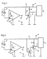
- the embodiment shown in Figure 1 of an inventive Circuit arrangement has an optical receiving part 1 in the form of a photodiode, the anode A at the input of a Amplifier circuit 2 and the cathode K on the one hand via a switch 3 with the supply voltage 4 and another with the control input B one through a switching transistor 5 trained quiescent current detector is connected.
- the circuit arrangement is in the idle state or the operating status.
- the quiescent current detector 5 follows the principle of the invention in the reverse direction operated, it locks both in the operating state and in Idle state of the circuit arrangement as long as no signal current the photodiode 1 is present.
- the base emitter path of the switching transistor 5 compensates the base emitter path of one Transistor 6 in a first stage of the amplifier circuit 2, so that when the switch 3 is open, the photodiode 1 according to the invention in photovoltaic mode, i.e. without bias can be held without this circuitry would be the internal voltage of the photodiode in photovoltaic mode less than the voltage of the base emitter path of the Transistor 6 and the photo current could not be tapped.
- the photocurrent of the photodiode 1 can now be switched through of the switching transistor 5 can be tapped due to this Switches signal through and so on line 7 via the high-resistance resistor 8 a start signal to a subsequent one Logic circuit 9 delivers.
- the logic circuit 9 can then the supply voltage 4 (for example +5 volts) over the Unlock switch 3 again. Then there is the Switching back to normal, ready-to-receive operating state, and the signals of diode 1 are through the amplifier 2 output to output 10.
- FIG. 2 shows a second exemplary embodiment of the invention, in which a pnp amplifying transistor 12 is connected after the pnp switching transistor 5 in a modification of the circuit arrangement according to FIG ), on which a control signal is tapped by the logic circuit 9 via the control line 7.
- This additional circuit is that the circuit becomes even more sensitive to light without additional quiescent current.
Landscapes
- Engineering & Computer Science (AREA)
- Computer Networks & Wireless Communication (AREA)
- Signal Processing (AREA)
- Physics & Mathematics (AREA)
- Electromagnetism (AREA)
- Electronic Switches (AREA)
- Dc Digital Transmission (AREA)
- Amplifiers (AREA)
Abstract
Claims (9)
- Circuit électronique comportant une partie de réception (1) qui saisit un signal physique arrivant de l'extérieur et fournit en réaction un signal de courant électrique, ainsi qu'une partie de commande et d'exploitation (2) associée à la partie de réception (1), alimentée par une tension d'alimentation (4), et recevant le courant électrique du signal, et dont la sortie de signal (10) fournit un signal de traitement électrique, le circuit pouvant passer dans un premier état de fonctionnement de travail lorsque la tension d'alimentation (4) est branchée et dans un second état de repos sans prise de puissance lorsque la tension d'alimentation (4) est coupée,
avec en parallèle au montage en série formé de la partie de réception (1) et de la partie de commande et d'exploitation (2), un détecteur de courant de repos (5) qui à l'état de repos du circuit, c'est-à-dire lorsque la tension d'alimentation (4) est coupée, saisit le courant du signal fourni par la partie de réception (1) et en réaction commande le branchement du circuit de commutation dans le mode de fonctionnement,
caractérisé en ce que
le détecteur de courant de repos (5) est formé par un commutateur commandé par le signal de courant et qui tant à l'état de repos qu'à l'état de fonctionnement bloque le circuit aussi longtemps qu'il n'y a pas de signal de courant, et qui (au repos du circuit) fournit un signal de commande en présence d'un signal de courant. - Circuit selon la revendication 1,
caractérisé en ce que
le détecteur de courant de repos (5) comporte un transistor de commutation dont la borne de commande (B) reçoit le signal de courant et dont une électrode est reliée à la masse et l'autre à la tension d'alimentation (4) par l'intermédiaire d'une résistance fortement ohmique (8). - Circuit selon l'une quelconque des revendications 1 ou 2,
caractérisé en ce que
la partie de réception (1) et la partie de commande et d'exploitation (2) sont réalisées par un ensemble fonctionnel à câblage fixe ayant uniquement trois bornes accessibles de l'extérieur, à savoir la masse (11), la sortie de signal (10) et la tension d'alimentation (4). - Circuit selon l'une quelconque des revendications 1 à 3,
caractérisé en ce qu'
un détecteur de repos (5) est branché en aval du circuit logique (9), ce circuit exploite le signal de commande fourni par le détecteur de courant de repos et le circuit logique est tenu sans courant, à l'état de repos du circuit et ce n'est qu'en présence d'un courant de repos qu'il se branche automatiquement. - Circuit selon l'une quelconque des revendications 2 à 4,
caractérisé en ce que
le transistor de commutation (5) fonctionne dans le sens du blocage de façon que dans chaque état de fonctionnement du circuit il se bloque aussi longtemps qu'il n'y a pas de courant de signal. - Circuit selon la revendication 5,
caractérisé en ce que
le transistor de commutation (5) est suivi d'un transistor amplificateur (12). - Circuit selon l'une quelconque des revendications précédentes,
caractérisé en ce que
la partie de réception (1) est réalisée par un photodétecteur, notamment une photodiode. - Circuit selon la revendication 7,
caractérisé en ce que
la partie de commande et d'exploitation (2) comprend le chemin base-émetteur d'un transistor (6), et au montage en série formé de la photodiode (1) et du chemin base-émetteur le détecteur de repos (5), parallèle comprend un transistor de commutation branché de manière complémentaire au chemin base-émetteur. - Circuit selon la revendication 8,
caractérisé en ce que
le chemin base-émetteur est formé par un transistor npn (6) et le transistor de commutation du détecteur de courant de repos (5) est formé par un transistor pnp (5).
Applications Claiming Priority (3)
| Application Number | Priority Date | Filing Date | Title |
|---|---|---|---|
| DE19839997A DE19839997C1 (de) | 1998-09-02 | 1998-09-02 | Elektronische Schaltungsanordnung |
| DE19839997 | 1998-09-02 | ||
| PCT/EP1999/006436 WO2000014889A1 (fr) | 1998-09-02 | 1999-09-01 | Circuit electrique |
Publications (2)
| Publication Number | Publication Date |
|---|---|
| EP1110329A1 EP1110329A1 (fr) | 2001-06-27 |
| EP1110329B1 true EP1110329B1 (fr) | 2002-12-18 |
Family
ID=7879569
Family Applications (1)
| Application Number | Title | Priority Date | Filing Date |
|---|---|---|---|
| EP99968744A Expired - Lifetime EP1110329B1 (fr) | 1998-09-02 | 1999-09-01 | Circuit electrique |
Country Status (5)
| Country | Link |
|---|---|
| US (1) | US6384662B1 (fr) |
| EP (1) | EP1110329B1 (fr) |
| DE (2) | DE19839997C1 (fr) |
| ES (1) | ES2185421T3 (fr) |
| WO (1) | WO2000014889A1 (fr) |
Families Citing this family (8)
| Publication number | Priority date | Publication date | Assignee | Title |
|---|---|---|---|---|
| DE20004444U1 (de) | 2000-03-09 | 2000-05-18 | Albert Ackermann GmbH & Co. KG, 51643 Gummersbach | Fernschalter |
| DE10056878A1 (de) * | 2000-11-16 | 2002-06-06 | Bosch Gmbh Robert | Ein stromfühlender Schalterstromkreis |
| US20040221959A1 (en) * | 2003-05-09 | 2004-11-11 | Applied Materials, Inc. | Anodized substrate support |
| TWI502984B (zh) * | 2012-11-23 | 2015-10-01 | Vivotek Inc | 網路攝影機驅動電路及其方法 |
| DE102016005321B4 (de) * | 2016-05-02 | 2017-11-23 | Keller Hcw Gmbh | Verfahren zur berührungslosen, strahlungsthermometrischen Temperaturmessung |
| DE102017122038A1 (de) | 2017-09-22 | 2019-03-28 | Osram Opto Semiconductors Gmbh | Sensor und Betriebsverfahren |
| JP6959297B2 (ja) * | 2019-05-23 | 2021-11-02 | 矢崎総業株式会社 | シートユニット |
| US11881731B2 (en) | 2020-04-15 | 2024-01-23 | Samsung Sdi Co., Ltd. | Control system for a battery system |
Family Cites Families (9)
| Publication number | Priority date | Publication date | Assignee | Title |
|---|---|---|---|---|
| NL8702749A (nl) * | 1987-11-18 | 1989-06-16 | Philips Nv | Afstandsbedieningssysteem met ontwaak signaal. |
| NL8802661A (nl) * | 1988-10-31 | 1990-05-16 | Philips Nv | Afstandsbedieningsontvanger met energie teruglevering aan batterij. |
| FR2660769B1 (fr) * | 1990-04-06 | 1994-09-23 | Neiman Sa | Circuit de reveil d'alimentation de microprocesseur, notamment pour une carte d'identification d'un ensemble de telecommande d'automobile. |
| JP3146716B2 (ja) * | 1993-02-10 | 2001-03-19 | 富士電機株式会社 | 光電変換回路 |
| DE19503243C2 (de) * | 1995-02-02 | 2000-08-03 | Loewe Opta Gmbh | Schaltungsanordnung |
| DE19645944A1 (de) * | 1996-11-07 | 1998-05-14 | Bosch Gmbh Robert | Steuergerät für ein Bordnetz |
| AT410620B (de) * | 1997-07-10 | 2003-06-25 | Efkon Entwicklung Forschung & Konstruktion Von Sondermaschinen Gmbh | Aufweckschaltung für ein elektronisches gerät |
| FI974225L (fi) * | 1997-11-13 | 1999-05-14 | Nokia Telecommunications Oy | Optinen vastaanotin |
| DE19844980C2 (de) * | 1998-09-30 | 2000-10-26 | Siemens Ag | Meßvorrichtung zur Messung der Zwischenkreisspannung von Gradientenverstärkern |
-
1998
- 1998-09-02 DE DE19839997A patent/DE19839997C1/de not_active Expired - Fee Related
-
1999
- 1999-09-01 EP EP99968744A patent/EP1110329B1/fr not_active Expired - Lifetime
- 1999-09-01 ES ES99968744T patent/ES2185421T3/es not_active Expired - Lifetime
- 1999-09-01 DE DE59903853T patent/DE59903853D1/de not_active Expired - Lifetime
- 1999-09-01 WO PCT/EP1999/006436 patent/WO2000014889A1/fr not_active Ceased
- 1999-09-01 US US09/786,268 patent/US6384662B1/en not_active Expired - Lifetime
Also Published As
| Publication number | Publication date |
|---|---|
| US6384662B1 (en) | 2002-05-07 |
| EP1110329A1 (fr) | 2001-06-27 |
| DE19839997C1 (de) | 2000-06-21 |
| WO2000014889A1 (fr) | 2000-03-16 |
| ES2185421T3 (es) | 2003-04-16 |
| DE59903853D1 (de) | 2003-01-30 |
Similar Documents
| Publication | Publication Date | Title |
|---|---|---|
| DE4008376C2 (fr) | ||
| EP0762651B1 (fr) | Circuit d'attaque pour une diode photoémettrice | |
| EP1110329B1 (fr) | Circuit electrique | |
| DE3929351C1 (fr) | ||
| DE2240181C2 (de) | Steuer- oder Regeleinrichtung mit einem Schalttransistor | |
| DE19811296A1 (de) | Integrierte Halbleiterschaltung | |
| DE69738366T2 (de) | Pull-Up-Schaltung und damit ausgerüstete Halbleitervorrichtung | |
| EP0444433B1 (fr) | Circuit pour trigger de Schmitt opto-électronique | |
| EP0583688B1 (fr) | Commutateur numérique de courant | |
| EP0393224B1 (fr) | Dispositif de contrôle de la température des transistors de puissance intégrés dans un circuit à semi-conducteurs | |
| DE69705928T2 (de) | Leuchtdiodenschaltung mit verringertem stromverbrauch | |
| CH644472A5 (de) | Optisch gekoppelter schalter mit einem feldeffekttransistor. | |
| DE102005013494B4 (de) | Optischer Empfänger | |
| EP0673118B1 (fr) | Convertisseur de niveau ECL en CMOS de type BiCMOS | |
| DE19962811B4 (de) | Gegentaktverstärkerschaltung | |
| DE3430338C2 (de) | Sendeschaltung für Signalübertragungssysteme | |
| EP0185377B1 (fr) | Circuit de signalisation | |
| EP0735493A1 (fr) | Circuit d'attaque de bus | |
| DE68916019T2 (de) | Verstärkeranordnung und verwendung in einer übertragungsleitungsschaltung. | |
| DE3920658C2 (de) | Vorrichtung zum Schutz von Ausgangstreibern vor Überlastung und Kurzschluß | |
| DE3335133C2 (fr) | ||
| DE69502057T2 (de) | Steuerschaltung für eine Vorspannungsquelle | |
| EP0548092B1 (fr) | Circuit de darlington avec dispositifs pour la detection d'une coupure dans son circuit de charge | |
| EP0588111B1 (fr) | Elément de mémoire | |
| EP0595831A1 (fr) | Circuit limiteur de la puissance du signal optique emis par un laser |
Legal Events
| Date | Code | Title | Description |
|---|---|---|---|
| PUAI | Public reference made under article 153(3) epc to a published international application that has entered the european phase |
Free format text: ORIGINAL CODE: 0009012 |
|
| 17P | Request for examination filed |
Effective date: 20010122 |
|
| AK | Designated contracting states |
Kind code of ref document: A1 Designated state(s): AT BE CH CY DE DK ES FI FR GB GR IE IT LI LU MC NL PT SE |
|
| GRAG | Despatch of communication of intention to grant |
Free format text: ORIGINAL CODE: EPIDOS AGRA |
|
| GRAG | Despatch of communication of intention to grant |
Free format text: ORIGINAL CODE: EPIDOS AGRA |
|
| GRAH | Despatch of communication of intention to grant a patent |
Free format text: ORIGINAL CODE: EPIDOS IGRA |
|
| 17Q | First examination report despatched |
Effective date: 20020305 |
|
| GRAH | Despatch of communication of intention to grant a patent |
Free format text: ORIGINAL CODE: EPIDOS IGRA |
|
| GRAA | (expected) grant |
Free format text: ORIGINAL CODE: 0009210 |
|
| AK | Designated contracting states |
Kind code of ref document: B1 Designated state(s): DE ES FR GB IT SE |
|
| REG | Reference to a national code |
Ref country code: GB Ref legal event code: FG4D Free format text: NOT ENGLISH |
|
| REG | Reference to a national code |
Ref country code: IE Ref legal event code: FG4D Free format text: GERMAN |
|
| REF | Corresponds to: |
Country of ref document: DE Kind code of ref document: P Ref document number: 59903853 Date of ref document: 20030130 |
|
| GBT | Gb: translation of ep patent filed (gb section 77(6)(a)/1977) |
Effective date: 20030206 |
|
| REG | Reference to a national code |
Ref country code: SE Ref legal event code: TRGR |
|
| REG | Reference to a national code |
Ref country code: ES Ref legal event code: FG2A Ref document number: 2185421 Country of ref document: ES Kind code of ref document: T3 |
|
| ET | Fr: translation filed | ||
| REG | Reference to a national code |
Ref country code: IE Ref legal event code: FD4D Ref document number: 1110329E Country of ref document: IE |
|
| PLBE | No opposition filed within time limit |
Free format text: ORIGINAL CODE: 0009261 |
|
| STAA | Information on the status of an ep patent application or granted ep patent |
Free format text: STATUS: NO OPPOSITION FILED WITHIN TIME LIMIT |
|
| 26N | No opposition filed |
Effective date: 20030919 |
|
| REG | Reference to a national code |
Ref country code: FR Ref legal event code: PLFP Year of fee payment: 18 |
|
| REG | Reference to a national code |
Ref country code: FR Ref legal event code: PLFP Year of fee payment: 19 |
|
| REG | Reference to a national code |
Ref country code: FR Ref legal event code: PLFP Year of fee payment: 20 |
|
| PGFP | Annual fee paid to national office [announced via postgrant information from national office to epo] |
Ref country code: DE Payment date: 20180921 Year of fee payment: 20 Ref country code: FR Payment date: 20180921 Year of fee payment: 20 Ref country code: IT Payment date: 20180921 Year of fee payment: 20 |
|
| PGFP | Annual fee paid to national office [announced via postgrant information from national office to epo] |
Ref country code: SE Payment date: 20180924 Year of fee payment: 20 Ref country code: GB Payment date: 20180924 Year of fee payment: 20 |
|
| PGFP | Annual fee paid to national office [announced via postgrant information from national office to epo] |
Ref country code: ES Payment date: 20181024 Year of fee payment: 20 |
|
| REG | Reference to a national code |
Ref country code: DE Ref legal event code: R071 Ref document number: 59903853 Country of ref document: DE |
|
| REG | Reference to a national code |
Ref country code: GB Ref legal event code: PE20 Expiry date: 20190831 |
|
| REG | Reference to a national code |
Ref country code: SE Ref legal event code: EUG |
|
| PG25 | Lapsed in a contracting state [announced via postgrant information from national office to epo] |
Ref country code: GB Free format text: LAPSE BECAUSE OF EXPIRATION OF PROTECTION Effective date: 20190831 |
|
| REG | Reference to a national code |
Ref country code: ES Ref legal event code: FD2A Effective date: 20220110 |
|
| PG25 | Lapsed in a contracting state [announced via postgrant information from national office to epo] |
Ref country code: ES Free format text: LAPSE BECAUSE OF EXPIRATION OF PROTECTION Effective date: 20190902 |