EP1111023A2 - Neutrale wassrige Suspension von kolloidalen Kieselsäure - Google Patents
Neutrale wassrige Suspension von kolloidalen Kieselsäure Download PDFInfo
- Publication number
- EP1111023A2 EP1111023A2 EP01101577A EP01101577A EP1111023A2 EP 1111023 A2 EP1111023 A2 EP 1111023A2 EP 01101577 A EP01101577 A EP 01101577A EP 01101577 A EP01101577 A EP 01101577A EP 1111023 A2 EP1111023 A2 EP 1111023A2
- Authority
- EP
- European Patent Office
- Prior art keywords
- suspension
- silicon
- polishing
- silica
- colloidal silica
- Prior art date
- Legal status (The legal status is an assumption and is not a legal conclusion. Google has not performed a legal analysis and makes no representation as to the accuracy of the status listed.)
- Granted
Links
Images

Classifications
-
- H—ELECTRICITY
- H10—SEMICONDUCTOR DEVICES; ELECTRIC SOLID-STATE DEVICES NOT OTHERWISE PROVIDED FOR
- H10P—GENERIC PROCESSES OR APPARATUS FOR THE MANUFACTURE OR TREATMENT OF DEVICES COVERED BY CLASS H10
- H10P52/00—Grinding, lapping or polishing of wafers, substrates or parts of devices
- H10P52/40—Chemomechanical polishing [CMP]
- H10P52/402—Chemomechanical polishing [CMP] of semiconductor materials
-
- H—ELECTRICITY
- H10—SEMICONDUCTOR DEVICES; ELECTRIC SOLID-STATE DEVICES NOT OTHERWISE PROVIDED FOR
- H10P—GENERIC PROCESSES OR APPARATUS FOR THE MANUFACTURE OR TREATMENT OF DEVICES COVERED BY CLASS H10
- H10P90/00—Preparation of wafers not covered by a single main group of this subclass, e.g. wafer reinforcement
- H10P90/12—Preparing bulk and homogeneous wafers
- H10P90/129—Preparing bulk and homogeneous wafers by polishing
-
- C—CHEMISTRY; METALLURGY
- C01—INORGANIC CHEMISTRY
- C01B—NON-METALLIC ELEMENTS; COMPOUNDS THEREOF; METALLOIDS OR COMPOUNDS THEREOF NOT COVERED BY SUBCLASS C01C
- C01B33/00—Silicon; Compounds thereof
- C01B33/113—Silicon oxides; Hydrates thereof
- C01B33/12—Silica; Hydrates thereof, e.g. lepidoic silicic acid
- C01B33/14—Colloidal silica, e.g. dispersions, gels, sols
- C01B33/141—Preparation of hydrosols or aqueous dispersions
- C01B33/142—Preparation of hydrosols or aqueous dispersions by acidic treatment of silicates
- C01B33/143—Preparation of hydrosols or aqueous dispersions by acidic treatment of silicates of aqueous solutions of silicates
-
- C—CHEMISTRY; METALLURGY
- C09—DYES; PAINTS; POLISHES; NATURAL RESINS; ADHESIVES; COMPOSITIONS NOT OTHERWISE PROVIDED FOR; APPLICATIONS OF MATERIALS NOT OTHERWISE PROVIDED FOR
- C09G—POLISHING COMPOSITIONS; SKI WAXES
- C09G1/00—Polishing compositions
- C09G1/02—Polishing compositions containing abrasives or grinding agents
-
- C—CHEMISTRY; METALLURGY
- C09—DYES; PAINTS; POLISHES; NATURAL RESINS; ADHESIVES; COMPOSITIONS NOT OTHERWISE PROVIDED FOR; APPLICATIONS OF MATERIALS NOT OTHERWISE PROVIDED FOR
- C09K—MATERIALS FOR MISCELLANEOUS APPLICATIONS, NOT PROVIDED FOR ELSEWHERE
- C09K3/00—Materials not provided for elsewhere
- C09K3/14—Anti-slip materials; Abrasives
- C09K3/1454—Abrasive powders, suspensions and pastes for polishing
- C09K3/1463—Aqueous liquid suspensions
-
- H—ELECTRICITY
- H10—SEMICONDUCTOR DEVICES; ELECTRIC SOLID-STATE DEVICES NOT OTHERWISE PROVIDED FOR
- H10P—GENERIC PROCESSES OR APPARATUS FOR THE MANUFACTURE OR TREATMENT OF DEVICES COVERED BY CLASS H10
- H10P52/00—Grinding, lapping or polishing of wafers, substrates or parts of devices
-
- H—ELECTRICITY
- H10—SEMICONDUCTOR DEVICES; ELECTRIC SOLID-STATE DEVICES NOT OTHERWISE PROVIDED FOR
- H10P—GENERIC PROCESSES OR APPARATUS FOR THE MANUFACTURE OR TREATMENT OF DEVICES COVERED BY CLASS H10
- H10P52/00—Grinding, lapping or polishing of wafers, substrates or parts of devices
- H10P52/40—Chemomechanical polishing [CMP]
- H10P52/403—Chemomechanical polishing [CMP] of conductive or resistive materials
-
- H—ELECTRICITY
- H10—SEMICONDUCTOR DEVICES; ELECTRIC SOLID-STATE DEVICES NOT OTHERWISE PROVIDED FOR
- H10P—GENERIC PROCESSES OR APPARATUS FOR THE MANUFACTURE OR TREATMENT OF DEVICES COVERED BY CLASS H10
- H10P90/00—Preparation of wafers not covered by a single main group of this subclass, e.g. wafer reinforcement
- H10P90/12—Preparing bulk and homogeneous wafers
-
- H—ELECTRICITY
- H10—SEMICONDUCTOR DEVICES; ELECTRIC SOLID-STATE DEVICES NOT OTHERWISE PROVIDED FOR
- H10P—GENERIC PROCESSES OR APPARATUS FOR THE MANUFACTURE OR TREATMENT OF DEVICES COVERED BY CLASS H10
- H10P95/00—Generic processes or apparatus for manufacture or treatments not covered by the other groups of this subclass
- H10P95/06—Planarisation of inorganic insulating materials
- H10P95/062—Planarisation of inorganic insulating materials involving a dielectric removal step
Definitions
- the present invention relates to a neutral aqueous suspension colloidal silica.
- a first job consists in the manufacture of plates for integrated circuits, that is to say the manufacture of silicon wafers. This is how that in this type of industry, we grow a silicon crystal, which we cut then in plates of about 750 micrometers thick, which are then subjected to a polishing so as to obtain a virgin silicon wafer polished. However, this type of industry does not manufacture integrated circuits and these plates for integrated circuits are sold to manufacturers of circuits integrated.
- US-A-3.170.273, US-A-4.664.679, US-A-4.117.093 and EP-A-0.684.638 describe the polishing of the initial silicon plates obtained at from the full crystal bar that is cut to obtain plates for integrated circuits.
- the second job that of manufacturers of integrated circuits, consists then in carrying out the integrated circuits, starting from the plates for integrated circuits obtained from the aforementioned manufacturers.
- the realization of integrated circuits implies in particular the following stages:
- the entire surface of the circuit boards integrated is oxidized to obtain an insulating layer.
- the zones thus engraved in hollow are called zones active.
- the present invention relates to polishing at this level of development of integrated circuits, as well as at the levels further development.
- steps of variable height are mainly generated by the etching steps, therefore hollow followed by a regular deposit.
- Reducing the dimensions of the transistors requires flattening these reliefs, because they can cause alignment difficulties (focusing during photolithography), problems of continuity of materials during deposits or residues of materials during the engraving of these materials.
- flattening is mainly done by mechanical-chemical polishing of the different layers deposited. Thickness remaining after polishing of these insulating deposits, semiconductors or conductors influences the electrical characteristics of integrated circuits.
- the manufacturing of integrated circuits is carried out, to date, on 200 mm diameter plates, with 50 to 200 circuits per next plate their size.
- aqueous suspensions of colloidal silica of basic pH the most often between pH 9 and pH 12.5.
- the pH of these aqueous suspensions colloidal silica was made basic by the addition of metal hydroxide alkaline such as sodium hydroxide or potassium hydroxide, or by the addition of a soluble amine in water (see in particular M.T. Bohr et al, WO-A-9627206, M. Motoshu and al, US-A-5.376.222, A.V. Gelatos et al, US-A-5.324.690, R.L. Lachapelle, US-A-3.328.141, S. Yamamichi et al, JP-A-07074313, M. Watanabe et al, JP-A-07249600).
- EP-A-0.745.656 describes the polishing of tiny insulators on a semiconductor substrate using an abrasive composition containing a mixture of aluminum oxide, silica and cerium oxide in the presence of a stabilizing agent.
- EP-A-0.363.100 describes the selective polishing between a surface comprising SI 3 N 4 and a surface more easily treatable than SI 3 N 4 using a colloidal silica with 95.3% purity and free of ammonia because of the drawbacks introduced by the latter on the selectivity of polishing.
- the main objective of the plaintiff is to point a polishing process which provides an improvement in the uniformity of polishing of the layers of the aforementioned materials installed on plates for integrated circuits, used as semiconductors or insulators in the manufacture of integrated circuits.
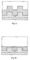
- polishing can be done on full plate (see figures Ia and Ib) or on plate with reliefs (see figures Ic and Id), in order to level these reliefs.
- the materials concerned by the invention integrate, as we have seen above, the materials based on silicon or based on doped silicon such as polycrystalline silicon, epitaxial silicon, amorphous silicon, glass phosphosilicate, or borophosphosilicate glass, the latter two being doped silicon oxide base, excluding the initial silicon used during the manufacture of plates for integrated circuits.
- doped silicon such as polycrystalline silicon, epitaxial silicon, amorphous silicon, glass phosphosilicate, or borophosphosilicate glass, the latter two being doped silicon oxide base, excluding the initial silicon used during the manufacture of plates for integrated circuits.
- a suspension of colloidal silica in particular a suspension comprising (or preferably essentially consisting of) fine individual particles of silica not linked together by siloxane bonds and used in neutral medium or close to neutrality, considerably improved the uniformity of polishing, while maintaining a good attack speed, as well as excellent planarization and surface qualities, in particular almost absence of roughness.
- it is meant by "essentially" more than 50%, in particular more than 60%, particularly more than 80%, more particularly more than 90%, especially more than 99%.
- abrasive which comprises an aqueous suspension at neutral pH or close to the neutrality of colloidal silica preferably containing silica particles individualized colloidal, not linked together by siloxane bonds, for chemical mechanical polishing of a layer of semiconductor material such than polycrystalline silicon, epitaxial monocrystalline silicon, silicon amorphous or insulating material such as phosphosilicate glass or glass of borophosphosilicate used during the manufacture of integrated circuits, with the exception of the initial silicon used during the manufacture of the plates for integrated circuits, as well as a chemical mechanical polishing process layer of semiconductor material such as polycrystalline silicon, silicon monocrystalline epitaxial, amorphous silicon or insulating material such as phosphosilicate glass or borophosphosilicate glass, used in the microelectronics industry of semiconductors, except silicon initial used in the manufacture of plates for integrated circuits, in which the layer of semiconductor material or layer is abraded insulating material by rubbing said layer using a fabric impre
- This chemical mechanical polishing can occur at different stages of the manufacture of integrated circuits, in particular in the stage lateral isolation of transistors, in the manufacture of transistor grids, in the manufacture of dielectric interconnections.
- This chemical mechanical polishing can also occur on full plate or plate with reliefs, to flatten them.
- aqueous suspensions of colloidal silica used preferably have individual particle diameters between 3 and 250 nm in particular between 7 and 150 nm, particularly between 10 and 100 nm.
- Preferred aqueous colloidal silica suspensions according to the invention are obtained either by neutralizing alkaline silica soils, particular, sodium or potassium, by an acid such as acid hydrochloric acid, nitric acid or sulfuric acid, either by neutralization of a acid silica sol with soda, potash or ammonia, preferably by potash and ammonia, and especially by ammonia.
- an acid such as acid hydrochloric acid, nitric acid or sulfuric acid
- aqueous suspensions with neutral pH are used or close to neutrality of colloidal silica having a pH between 6 and 8, particularly between 6.5 and 7.5.
- the diameters of the elementary particles of the colloidal silica suspensions are between 3 and 250 nm, particularly between 10 and 100 nm.
- the weight concentration of product of polishing is from 5 to 50%, preferably from 15 to 40%.
- a main advantage of the invention is the improvement of uniformity of chemical mechanical polishing of layers of semiconductor material such as polysilicon (polycrystalline silicon) or insulators doped silicon oxide base such as boro phosphosilicate glass (BPSG) by using aqueous suspensions of colloidal silica at pH neutral or close to neutrality.
- semiconductor material such as polysilicon (polycrystalline silicon) or insulators doped silicon oxide base such as boro phosphosilicate glass (BPSG)
- This improvement can for example be essentially demonstrated by tests of uniformity of attack of the polishing while maintaining an acceptable speed of attack of the semiconductor material.
- suspensions aqueous at neutral pH or close to neutrality of colloidal silica in particular made up of individual particles, not linked together by siloxane bonds, have very good stability over time, whence results the absence of sedimentation of the particles during the storage time.
- the present application finally relates to an abrasive for chemical mechanical polishing of a layer of semiconductor material based of silicon such as polycrystalline silicon, epitaxial silicon or silicon amorphous or insulators based on doped silicon oxide such as glass phosphosilicate (PSG) or borophosphosilicate glass (BPSG), to with the exception of the initial silicon used during the manufacture of the plates for integrated circuits, comprising a fabric impregnated with a liquid composition abrasive containing an aqueous suspension at neutral pH or close to the neutrality of colloidal silica, preferably comprising particles individualized not linked together by siloxane bonds, of diameter between 3 and 250 nanometers, pH between 6 and 8.
- silicon oxide such as glass phosphosilicate (PSG) or borophosphosilicate glass (BPSG)
- PSG glass phosphosilicate
- BPSG borophosphosilicate glass
- Figure la illustrates the state of a full plate coated with polysilicon before polishing
- figure Ib illustrates the state of this plate after polishing.
- Figures Ic and Id illustrate the state of a similar plate but with reliefs. These reliefs were dug by photo lithography.
- Example of polishing with suspension-based abrasives aqueous with neutral pH of colloidal silica.
- a polysilicon deposit is made on each wafer studied about 0.4 ⁇ m which is measured before and after polishing.
- polishing with suspension-based abrasives aqueous near colloidal silica neutrality.
- BPSG borophosphosilicate glass
- Example of polishing with suspension-based abrasives basic aqueous colloidal silica.
- Example of polishing with suspension-based abrasives aqueous colloidal silica acids.
- BPSG borophosphosilicate glass
- BPSG borophosphosilicate glass
- silica suspensions colloidal at neutral pH or close to neutrality provides good uniformity of polishing both on polysilicon and on BPSG while maintaining a good attack speed, a very good surface condition of the plate and excellent flattening.
Landscapes
- Chemical & Material Sciences (AREA)
- Organic Chemistry (AREA)
- Dispersion Chemistry (AREA)
- Inorganic Chemistry (AREA)
- Engineering & Computer Science (AREA)
- Materials Engineering (AREA)
- Mechanical Treatment Of Semiconductor (AREA)
- Finish Polishing, Edge Sharpening, And Grinding By Specific Grinding Devices (AREA)
- Silicon Compounds (AREA)
Applications Claiming Priority (3)
| Application Number | Priority Date | Filing Date | Title |
|---|---|---|---|
| FR9704207 | 1997-04-07 | ||
| FR9704207A FR2761629B1 (fr) | 1997-04-07 | 1997-04-07 | Nouveau procede de polissage mecano-chimique de couches de materiaux semi-conducteurs a base de polysilicium ou d'oxyde de silicium dope |
| EP98400715A EP0878838B1 (de) | 1997-04-07 | 1998-03-26 | Verfahren zum chemisch-mechanischen Polieren von halbleitenden oder isolierenden Schichten |
Related Parent Applications (2)
| Application Number | Title | Priority Date | Filing Date |
|---|---|---|---|
| EP98400715.3 Division | 1998-03-26 | ||
| EP98400715A Division EP0878838B1 (de) | 1997-04-07 | 1998-03-26 | Verfahren zum chemisch-mechanischen Polieren von halbleitenden oder isolierenden Schichten |
Publications (3)
| Publication Number | Publication Date |
|---|---|
| EP1111023A2 true EP1111023A2 (de) | 2001-06-27 |
| EP1111023A3 EP1111023A3 (de) | 2008-01-23 |
| EP1111023B1 EP1111023B1 (de) | 2011-10-05 |
Family
ID=9505584
Family Applications (2)
| Application Number | Title | Priority Date | Filing Date |
|---|---|---|---|
| EP01101577A Expired - Lifetime EP1111023B1 (de) | 1997-04-07 | 1998-03-26 | Neutrale wassrige Suspension von kolloidalen Kieselsäure |
| EP98400715A Expired - Lifetime EP0878838B1 (de) | 1997-04-07 | 1998-03-26 | Verfahren zum chemisch-mechanischen Polieren von halbleitenden oder isolierenden Schichten |
Family Applications After (1)
| Application Number | Title | Priority Date | Filing Date |
|---|---|---|---|
| EP98400715A Expired - Lifetime EP0878838B1 (de) | 1997-04-07 | 1998-03-26 | Verfahren zum chemisch-mechanischen Polieren von halbleitenden oder isolierenden Schichten |
Country Status (10)
| Country | Link |
|---|---|
| US (1) | US6126518A (de) |
| EP (2) | EP1111023B1 (de) |
| JP (1) | JP4233629B2 (de) |
| KR (1) | KR100510951B1 (de) |
| CN (1) | CN1152416C (de) |
| AT (2) | ATE291277T1 (de) |
| DE (1) | DE69829329T2 (de) |
| FR (1) | FR2761629B1 (de) |
| MY (1) | MY119523A (de) |
| SG (1) | SG77633A1 (de) |
Families Citing this family (21)
| Publication number | Priority date | Publication date | Assignee | Title |
|---|---|---|---|---|
| FR2781922B1 (fr) | 1998-07-31 | 2001-11-23 | Clariant France Sa | Procede de polissage mecano-chimique d'une couche en un materiau a base de cuivre |
| FR2785614B1 (fr) | 1998-11-09 | 2001-01-26 | Clariant France Sa | Nouveau procede de polissage mecano-chimique selectif entre une couche d'oxyde de silicium et une couche de nitrure de silicium |
| FR2792643B1 (fr) * | 1999-04-22 | 2001-07-27 | Clariant France Sa | Composition de polissage mecano-chimique de couches en un materiau isolant a base de polymere a faible constante dielectrique |
| JP2002050594A (ja) * | 2000-08-04 | 2002-02-15 | Fuso Chemical Co Ltd | コロイド状シリカスラリー |
| FR2819244B1 (fr) * | 2001-01-09 | 2003-04-11 | Clariant France Sa | Nouvelles suspensions aqueuses de silice colloidale anionique de ph neutre et leur procede de preparation, et leurs applications |
| FR2819245B1 (fr) * | 2001-01-09 | 2004-11-26 | Clariant | Nouvelles suspensions aqueuses de silice colloidale anionique de ph neutre et leur procede de preparation, et leurs applications |
| US6939203B2 (en) * | 2002-04-18 | 2005-09-06 | Asm Nutool, Inc. | Fluid bearing slide assembly for workpiece polishing |
| US20070286773A1 (en) * | 2002-05-16 | 2007-12-13 | Micronit Microfluidics B.V. | Microfluidic Device |
| DE60228685D1 (de) * | 2002-05-16 | 2008-10-16 | Micronit Microfluidics Bv | Verfahren zur Herstellung eines mikrofluidischen Bauteiles |
| TW200401816A (en) * | 2002-06-03 | 2004-02-01 | Shipley Co Llc | Electronic device manufacture |
| KR101004525B1 (ko) * | 2002-08-19 | 2010-12-31 | 호야 가부시키가이샤 | 마스크 블랭크용 글래스 기판 제조 방법, 마스크 블랭크제조방법, 전사 마스크 제조 방법, 반도체 디바이스제조방법, 마스크 블랭크용 글래스 기판, 마스크 블랭크,및 전사 마스크 |
| FR2857895B1 (fr) * | 2003-07-23 | 2007-01-26 | Soitec Silicon On Insulator | Procede de preparation de surface epiready sur films minces de sic |
| US20080220610A1 (en) * | 2006-06-29 | 2008-09-11 | Cabot Microelectronics Corporation | Silicon oxide polishing method utilizing colloidal silica |
| EP2063461A4 (de) * | 2006-09-13 | 2010-06-02 | Asahi Glass Co Ltd | Poliermittel für ein integriertes halbleiterschaltungsbauelement, polierverfahren und verfahren zum herstellen eines integrierten halbleiterschaltungsbauelements |
| JP4411331B2 (ja) * | 2007-03-19 | 2010-02-10 | 信越化学工業株式会社 | 磁気記録媒体用シリコン基板およびその製造方法 |
| CN101821835B (zh) * | 2007-09-28 | 2013-03-27 | 霓达哈斯股份有限公司 | 研磨用组合物 |
| DE102011079694A1 (de) | 2011-07-25 | 2013-01-31 | Carl Zeiss Smt Gmbh | Verfahren zum Polieren einer Schicht aus amorphem Silizium |
| CN107953225A (zh) * | 2016-10-14 | 2018-04-24 | 上海新昇半导体科技有限公司 | 半导体晶圆的抛光方法 |
| JP7528681B2 (ja) * | 2020-09-29 | 2024-08-06 | 住友金属鉱山株式会社 | SiC多結晶基板の研磨方法 |
| CN113045992A (zh) * | 2021-03-23 | 2021-06-29 | 广东精坚科技有限公司 | 一种中性抛光液及其制备方法 |
| CN114744065B (zh) * | 2022-03-23 | 2024-06-14 | 中国电子科技集团公司第十一研究所 | 台面结构芯片的非接触式光刻方法 |
Family Cites Families (20)
| Publication number | Priority date | Publication date | Assignee | Title |
|---|---|---|---|---|
| US35420A (en) * | 1862-05-27 | And bdwaed joslin | ||
| US2744001A (en) * | 1950-09-08 | 1956-05-01 | Rare Earths Inc | Polishing material and method of making same |
| US2680721A (en) * | 1952-03-20 | 1954-06-08 | Du Pont | Process of increasing the size of unaggregated silica particles in an aqueous silicasuspension |
| NL213258A (de) * | 1955-12-22 | |||
| US3208823A (en) * | 1958-10-20 | 1965-09-28 | Philadelphia Quartz Co | Finely divided silica product and its method of preparation |
| US3170273A (en) * | 1963-01-10 | 1965-02-23 | Monsanto Co | Process for polishing semiconductor materials |
| US3440174A (en) * | 1965-04-26 | 1969-04-22 | Nalco Chemical Co | Method of making silica sols containing large particle size silica |
| US3867304A (en) * | 1967-06-12 | 1975-02-18 | Nalco Chemical Co | Acidic stable salt-free silica sols |
| US3715842A (en) * | 1970-07-02 | 1973-02-13 | Tizon Chem Corp | Silica polishing compositions having a reduced tendency to scratch silicon and germanium surfaces |
| DE2629709C2 (de) * | 1976-07-02 | 1982-06-03 | Ibm Deutschland Gmbh, 7000 Stuttgart | Verfahren zur Herstellung eines metallionenfreien amorphen Siliciumdioxids und daraus hergestelltes Poliermittel zum mechanischen Polieren von Halbleiteroberflächen |
| US4435247A (en) * | 1983-03-10 | 1984-03-06 | International Business Machines Corporation | Method for polishing titanium carbide |
| JPS61136909A (ja) * | 1984-12-04 | 1986-06-24 | Mitsubishi Chem Ind Ltd | 無水ケイ酸の水分散液組成物 |
| JPH02209730A (ja) * | 1988-10-02 | 1990-08-21 | Canon Inc | 選択研磨法 |
| USRE35420E (en) | 1991-02-11 | 1997-01-07 | Micron Technology, Inc. | Method of increasing capacitance by surface roughening in semiconductor wafer processing |
| US5395801A (en) * | 1993-09-29 | 1995-03-07 | Micron Semiconductor, Inc. | Chemical-mechanical polishing processes of planarizing insulating layers |
| JP2719113B2 (ja) * | 1994-05-24 | 1998-02-25 | 信越半導体株式会社 | 単結晶シリコンウェーハの歪付け方法 |
| KR960041316A (ko) * | 1995-05-22 | 1996-12-19 | 고사이 아키오 | 연마용 입상체, 이의 제조방법 및 이의 용도 |
| US5575706A (en) * | 1996-01-11 | 1996-11-19 | Taiwan Semiconductor Manufacturing Company Ltd. | Chemical/mechanical planarization (CMP) apparatus and polish method |
| DE19623062C2 (de) * | 1996-06-10 | 1998-07-02 | Bayer Ag | Verfahren zur Herstellung salzarmer Kieselsoldispersionen in niedrigsiedenden Alkoholen |
| US5738800A (en) * | 1996-09-27 | 1998-04-14 | Rodel, Inc. | Composition and method for polishing a composite of silica and silicon nitride |
-
1997
- 1997-04-07 FR FR9704207A patent/FR2761629B1/fr not_active Expired - Lifetime
-
1998
- 1998-03-26 AT AT98400715T patent/ATE291277T1/de active
- 1998-03-26 EP EP01101577A patent/EP1111023B1/de not_active Expired - Lifetime
- 1998-03-26 EP EP98400715A patent/EP0878838B1/de not_active Expired - Lifetime
- 1998-03-26 AT AT01101577T patent/ATE527211T1/de active
- 1998-03-26 DE DE69829329T patent/DE69829329T2/de not_active Expired - Lifetime
- 1998-04-03 US US09/054,518 patent/US6126518A/en not_active Expired - Lifetime
- 1998-04-04 MY MYPI98001512A patent/MY119523A/en unknown
- 1998-04-06 SG SG1998000701A patent/SG77633A1/en unknown
- 1998-04-06 JP JP9296598A patent/JP4233629B2/ja not_active Expired - Lifetime
- 1998-04-06 KR KR10-1998-0012061A patent/KR100510951B1/ko not_active Expired - Lifetime
- 1998-04-07 CN CNB98109693XA patent/CN1152416C/zh not_active Expired - Lifetime
Also Published As
| Publication number | Publication date |
|---|---|
| FR2761629A1 (fr) | 1998-10-09 |
| CN1208248A (zh) | 1999-02-17 |
| ATE291277T1 (de) | 2005-04-15 |
| KR19980081128A (ko) | 1998-11-25 |
| DE69829329D1 (de) | 2005-04-21 |
| EP0878838A2 (de) | 1998-11-18 |
| CN1152416C (zh) | 2004-06-02 |
| EP1111023A3 (de) | 2008-01-23 |
| KR100510951B1 (ko) | 2005-11-21 |
| HK1018540A1 (en) | 1999-12-24 |
| EP0878838A3 (de) | 1998-12-16 |
| JPH10308379A (ja) | 1998-11-17 |
| FR2761629B1 (fr) | 1999-06-18 |
| DE69829329T2 (de) | 2006-04-13 |
| ATE527211T1 (de) | 2011-10-15 |
| JP4233629B2 (ja) | 2009-03-04 |
| SG77633A1 (en) | 2001-01-16 |
| EP0878838B1 (de) | 2005-03-16 |
| MY119523A (en) | 2005-06-30 |
| US6126518A (en) | 2000-10-03 |
| EP1111023B1 (de) | 2011-10-05 |
Similar Documents
| Publication | Publication Date | Title |
|---|---|---|
| EP0878838B1 (de) | Verfahren zum chemisch-mechanischen Polieren von halbleitenden oder isolierenden Schichten | |
| US6267909B1 (en) | Planarization composition for removing metal films | |
| US7029373B2 (en) | Chemical mechanical polishing compositions for metal and associated materials and method of using same | |
| US6692546B2 (en) | Chemical mechanical polishing compositions for metal and associated materials and method of using same | |
| EP1090083B1 (de) | Suspension zum chemisch-mechanischen polieren von kupfer/tantalum-substraten | |
| TWI434955B (zh) | 含鎢基材的化學機械平坦化方法 | |
| US20210340445A1 (en) | Tungsten Chemical Mechanical Planarization (CMP) With Low Dishing And Low Erosion Topography | |
| CA2335035A1 (en) | Chemical mechanical polishing slurry and method for using same | |
| KR102312219B1 (ko) | 화학 기계적 연마 텅스텐 버핑 슬러리 | |
| JPH10308379A5 (de) | ||
| CN111944428B (zh) | 化学机械抛光组合物以及优先于二氧化硅抛光氮化硅并同时抑制对二氧化硅的损伤的方法 | |
| TW202104524A (zh) | 具有增強的缺陷抑制並且在酸性環境中優先於二氧化矽選擇性地拋光氮化矽之化學機械拋光組成物及方法 | |
| EP0838845B1 (de) | Neues Verfahren zum chemisch mechanischen Polieren von Isolationsschichten aus Silizium oder Silizium enthaltenden Materialien | |
| US11066575B2 (en) | Chemical mechanical planarization for tungsten-containing substrates | |
| CN112552824A (zh) | 研磨用组合物和研磨方法 | |
| US20040237413A1 (en) | Chemical mechanical polishing agent kit and chemical mechanical polishing method using the same | |
| US20080182413A1 (en) | Selective chemistry for fixed abrasive cmp | |
| EP3702424B1 (de) | Chemischer und mechanischer polierschlamm zur isolierung von flachen gräben | |
| EP4048746A1 (de) | Chemisch-mechanische planarisierungszusammensetzungen mit hoher oxidentfernungsrate zur isolierung flacher graben | |
| FR2835844A1 (fr) | Procede de polissage mecano-chimique de substrats metalliques | |
| KR100449610B1 (ko) | 절연층 연마용 슬러리 조성물 | |
| EP4157955A1 (de) | Cmp-polierzusammensetzungen mit niedrigem muldenbildungsoxid für flache grabenisolationsanwendungen und verfahren zur herstellung davon | |
| CN114787304A (zh) | 低氧化物沟槽凹陷的浅沟槽隔离化学机械平面化抛光 | |
| WO2026024385A1 (en) | Oxide polishing compositions and polishing methods | |
| EP3689988A1 (de) | Chemisch-mechanisches planarisierungs(cmp)-polieren durch flache grabenisolation mit abstimmbaren siliziumoxid- und siliziumnitridabtragsraten |
Legal Events
| Date | Code | Title | Description |
|---|---|---|---|
| PUAI | Public reference made under article 153(3) epc to a published international application that has entered the european phase |
Free format text: ORIGINAL CODE: 0009012 |
|
| AC | Divisional application: reference to earlier application |
Ref document number: 878838 Country of ref document: EP |
|
| AK | Designated contracting states |
Kind code of ref document: A2 Designated state(s): AT BE CH DE DK ES FI FR GB IE IT LI LU MC NL SE |
|
| RAP1 | Party data changed (applicant data changed or rights of an application transferred) |
Owner name: CLARIANT FINANCE (BVI) LIMITED |
|
| RAP1 | Party data changed (applicant data changed or rights of an application transferred) |
Owner name: AZ ELECTRONIC MATERIALS USA CORP. |
|
| PUAL | Search report despatched |
Free format text: ORIGINAL CODE: 0009013 |
|
| RIC1 | Information provided on ipc code assigned before grant |
Ipc: C01B 33/141 20060101AFI20071205BHEP Ipc: C01B 33/148 20060101ALI20071205BHEP |
|
| AK | Designated contracting states |
Kind code of ref document: A3 Designated state(s): AT BE CH DE DK ES FI FR GB IE IT LI LU MC NL SE |
|
| 17P | Request for examination filed |
Effective date: 20080710 |
|
| AKX | Designation fees paid |
Designated state(s): AT BE CH DE DK ES FI FR GB IE IT LI LU MC NL SE |
|
| 17Q | First examination report despatched |
Effective date: 20081114 |
|
| GRAP | Despatch of communication of intention to grant a patent |
Free format text: ORIGINAL CODE: EPIDOSNIGR1 |
|
| GRAS | Grant fee paid |
Free format text: ORIGINAL CODE: EPIDOSNIGR3 |
|
| GRAA | (expected) grant |
Free format text: ORIGINAL CODE: 0009210 |
|
| AC | Divisional application: reference to earlier application |
Ref document number: 0878838 Country of ref document: EP Kind code of ref document: P |
|
| AK | Designated contracting states |
Kind code of ref document: B1 Designated state(s): AT BE CH DE DK ES FI FR GB IE IT LI LU MC NL SE |
|
| REG | Reference to a national code |
Ref country code: GB Ref legal event code: FG4D Free format text: NOT ENGLISH |
|
| REG | Reference to a national code |
Ref country code: CH Ref legal event code: EP |
|
| REG | Reference to a national code |
Ref country code: IE Ref legal event code: FG4D |
|
| REG | Reference to a national code |
Ref country code: DE Ref legal event code: R096 Ref document number: 69842438 Country of ref document: DE Effective date: 20111124 |
|
| REG | Reference to a national code |
Ref country code: NL Ref legal event code: T3 |
|
| PG25 | Lapsed in a contracting state [announced via postgrant information from national office to epo] |
Ref country code: SE Free format text: LAPSE BECAUSE OF FAILURE TO SUBMIT A TRANSLATION OF THE DESCRIPTION OR TO PAY THE FEE WITHIN THE PRESCRIBED TIME-LIMIT Effective date: 20111005 |
|
| PG25 | Lapsed in a contracting state [announced via postgrant information from national office to epo] |
Ref country code: DK Free format text: LAPSE BECAUSE OF FAILURE TO SUBMIT A TRANSLATION OF THE DESCRIPTION OR TO PAY THE FEE WITHIN THE PRESCRIBED TIME-LIMIT Effective date: 20111005 |
|
| PLBE | No opposition filed within time limit |
Free format text: ORIGINAL CODE: 0009261 |
|
| STAA | Information on the status of an ep patent application or granted ep patent |
Free format text: STATUS: NO OPPOSITION FILED WITHIN TIME LIMIT |
|
| PG25 | Lapsed in a contracting state [announced via postgrant information from national office to epo] |
Ref country code: IT Free format text: LAPSE BECAUSE OF FAILURE TO SUBMIT A TRANSLATION OF THE DESCRIPTION OR TO PAY THE FEE WITHIN THE PRESCRIBED TIME-LIMIT Effective date: 20111005 |
|
| 26N | No opposition filed |
Effective date: 20120706 |
|
| PG25 | Lapsed in a contracting state [announced via postgrant information from national office to epo] |
Ref country code: MC Free format text: LAPSE BECAUSE OF NON-PAYMENT OF DUE FEES Effective date: 20120331 |
|
| REG | Reference to a national code |
Ref country code: CH Ref legal event code: PL Ref country code: DE Ref legal event code: R097 Ref document number: 69842438 Country of ref document: DE Effective date: 20120706 |
|
| PG25 | Lapsed in a contracting state [announced via postgrant information from national office to epo] |
Ref country code: LI Free format text: LAPSE BECAUSE OF NON-PAYMENT OF DUE FEES Effective date: 20120331 Ref country code: CH Free format text: LAPSE BECAUSE OF NON-PAYMENT OF DUE FEES Effective date: 20120331 |
|
| PG25 | Lapsed in a contracting state [announced via postgrant information from national office to epo] |
Ref country code: ES Free format text: LAPSE BECAUSE OF FAILURE TO SUBMIT A TRANSLATION OF THE DESCRIPTION OR TO PAY THE FEE WITHIN THE PRESCRIBED TIME-LIMIT Effective date: 20120116 |
|
| PG25 | Lapsed in a contracting state [announced via postgrant information from national office to epo] |
Ref country code: LU Free format text: LAPSE BECAUSE OF NON-PAYMENT OF DUE FEES Effective date: 20120326 |
|
| REG | Reference to a national code |
Ref country code: DE Ref legal event code: R082 Ref document number: 69842438 Country of ref document: DE Representative=s name: PATENTANWAELTE ISENBRUCK BOESL HOERSCHLER LLP, DE |
|
| REG | Reference to a national code |
Ref country code: GB Ref legal event code: 732E Free format text: REGISTERED BETWEEN 20150205 AND 20150211 |
|
| REG | Reference to a national code |
Ref country code: FR Ref legal event code: TP Owner name: MERCK PATENT GMBH, DE Effective date: 20150204 |
|
| REG | Reference to a national code |
Ref country code: AT Ref legal event code: PC Ref document number: 527211 Country of ref document: AT Kind code of ref document: T Owner name: MERCK PATENT GMBH, DE Effective date: 20150123 |
|
| REG | Reference to a national code |
Ref country code: NL Ref legal event code: SD Effective date: 20150324 |
|
| REG | Reference to a national code |
Ref country code: DE Ref legal event code: R082 Ref document number: 69842438 Country of ref document: DE Representative=s name: PATENTANWAELTE ISENBRUCK BOESL HOERSCHLER LLP, DE Effective date: 20150223 Ref country code: DE Ref legal event code: R081 Ref document number: 69842438 Country of ref document: DE Owner name: MERCK PATENT GMBH, DE Free format text: FORMER OWNER: CLARIANT (FRANCE) S.A., PUTEAUX, FR Effective date: 20111006 Ref country code: DE Ref legal event code: R081 Ref document number: 69842438 Country of ref document: DE Owner name: MERCK PATENT GMBH, DE Free format text: FORMER OWNER: AZ ELECTRONIC MATERIALS USA CORP., SOMERVILLE, N.J., US Effective date: 20150223 |
|
| REG | Reference to a national code |
Ref country code: FR Ref legal event code: PLFP Year of fee payment: 19 |
|
| REG | Reference to a national code |
Ref country code: FR Ref legal event code: PLFP Year of fee payment: 20 |
|
| PGFP | Annual fee paid to national office [announced via postgrant information from national office to epo] |
Ref country code: DE Payment date: 20170321 Year of fee payment: 20 Ref country code: FR Payment date: 20170213 Year of fee payment: 20 Ref country code: FI Payment date: 20170309 Year of fee payment: 20 |
|
| PGFP | Annual fee paid to national office [announced via postgrant information from national office to epo] |
Ref country code: NL Payment date: 20170210 Year of fee payment: 20 Ref country code: IE Payment date: 20170309 Year of fee payment: 20 Ref country code: AT Payment date: 20170227 Year of fee payment: 20 Ref country code: BE Payment date: 20170124 Year of fee payment: 20 Ref country code: GB Payment date: 20170322 Year of fee payment: 20 |
|
| REG | Reference to a national code |
Ref country code: DE Ref legal event code: R071 Ref document number: 69842438 Country of ref document: DE |
|
| REG | Reference to a national code |
Ref country code: NL Ref legal event code: MK Effective date: 20180325 |
|
| REG | Reference to a national code |
Ref country code: BE Ref legal event code: MK Effective date: 20180326 Ref country code: BE Ref legal event code: PD Owner name: MERCK PATENT GMBH; DE Free format text: DETAILS ASSIGNMENT: CHANGE OF OWNER(S), AFFECTATION / CESSION; FORMER OWNER NAME: AZ ELECTRONIC MATERIALS USA CORP. Effective date: 20150121 |
|
| REG | Reference to a national code |
Ref country code: GB Ref legal event code: PE20 Expiry date: 20180325 |
|
| PG25 | Lapsed in a contracting state [announced via postgrant information from national office to epo] |
Ref country code: GB Free format text: LAPSE BECAUSE OF EXPIRATION OF PROTECTION Effective date: 20180325 |
|
| REG | Reference to a national code |
Ref country code: IE Ref legal event code: MK9A |
|
| REG | Reference to a national code |
Ref country code: AT Ref legal event code: MK07 Ref document number: 527211 Country of ref document: AT Kind code of ref document: T Effective date: 20180326 |
|
| PG25 | Lapsed in a contracting state [announced via postgrant information from national office to epo] |
Ref country code: IE Free format text: LAPSE BECAUSE OF EXPIRATION OF PROTECTION Effective date: 20180326 |