EP1111409A2 - Méthode de marquage - Google Patents
Méthode de marquage Download PDFInfo
- Publication number
- EP1111409A2 EP1111409A2 EP00660232A EP00660232A EP1111409A2 EP 1111409 A2 EP1111409 A2 EP 1111409A2 EP 00660232 A EP00660232 A EP 00660232A EP 00660232 A EP00660232 A EP 00660232A EP 1111409 A2 EP1111409 A2 EP 1111409A2
- Authority
- EP
- European Patent Office
- Prior art keywords
- coating
- given
- identifier
- object according
- order
- Prior art date
- Legal status (The legal status is an assumption and is not a legal conclusion. Google has not performed a legal analysis and makes no representation as to the accuracy of the status listed.)
- Withdrawn
Links
Images


Classifications
-
- H—ELECTRICITY
- H04—ELECTRIC COMMUNICATION TECHNIQUE
- H04B—TRANSMISSION
- H04B1/00—Details of transmission systems, not covered by a single one of groups H04B3/00 - H04B13/00; Details of transmission systems not characterised by the medium used for transmission
- H04B1/38—Transceivers, i.e. devices in which transmitter and receiver form a structural unit and in which at least one part is used for functions of transmitting and receiving
- H04B1/3827—Portable transceivers
- H04B1/3888—Arrangements for carrying or protecting transceivers
-
- A—HUMAN NECESSITIES
- A45—HAND OR TRAVELLING ARTICLES
- A45C—PURSES; LUGGAGE; HAND CARRIED BAGS
- A45C13/00—Details; Accessories
- A45C13/08—Decorative devices for handbags or purses
-
- G—PHYSICS
- G02—OPTICS
- G02B—OPTICAL ELEMENTS, SYSTEMS OR APPARATUS
- G02B5/00—Optical elements other than lenses
- G02B5/20—Filters
- G02B5/28—Interference filters
- G02B5/285—Interference filters comprising deposited thin solid films
- G02B5/286—Interference filters comprising deposited thin solid films having four or fewer layers, e.g. for achieving a colour effect
-
- Y—GENERAL TAGGING OF NEW TECHNOLOGICAL DEVELOPMENTS; GENERAL TAGGING OF CROSS-SECTIONAL TECHNOLOGIES SPANNING OVER SEVERAL SECTIONS OF THE IPC; TECHNICAL SUBJECTS COVERED BY FORMER USPC CROSS-REFERENCE ART COLLECTIONS [XRACs] AND DIGESTS
- Y10—TECHNICAL SUBJECTS COVERED BY FORMER USPC
- Y10T—TECHNICAL SUBJECTS COVERED BY FORMER US CLASSIFICATION
- Y10T428/00—Stock material or miscellaneous articles
- Y10T428/24—Structurally defined web or sheet [e.g., overall dimension, etc.]
- Y10T428/24802—Discontinuous or differential coating, impregnation or bond [e.g., artwork, printing, retouched photograph, etc.]
- Y10T428/24926—Discontinuous or differential coating, impregnation or bond [e.g., artwork, printing, retouched photograph, etc.] including ceramic, glass, porcelain or quartz layer
-
- Y—GENERAL TAGGING OF NEW TECHNOLOGICAL DEVELOPMENTS; GENERAL TAGGING OF CROSS-SECTIONAL TECHNOLOGIES SPANNING OVER SEVERAL SECTIONS OF THE IPC; TECHNICAL SUBJECTS COVERED BY FORMER USPC CROSS-REFERENCE ART COLLECTIONS [XRACs] AND DIGESTS
- Y10—TECHNICAL SUBJECTS COVERED BY FORMER USPC
- Y10T—TECHNICAL SUBJECTS COVERED BY FORMER US CLASSIFICATION
- Y10T428/00—Stock material or miscellaneous articles
- Y10T428/26—Web or sheet containing structurally defined element or component, the element or component having a specified physical dimension
Definitions
- the invention relates to changing the visual appearance of optical surfaces and/or other structures.
- the image of a product includes a given appearance, and special features in said appearance can be used for emphasising the characteristics of the product, for instance the impression of high technology.
- Coating the reflective surfaces of telescope mirrors with silver, as well as other optical coating operations, such as aluminising by vaporising in a vacuum, are known techniques for achieving an advantageous optical coating.
- CVD and PVD processes are methods known as such in the growing of film-like surfaces, for instance in connection with the production of semiconductors or their microstructures.
- the object of the invention is to achieve for the product an artistic and pleasant appearance with a certain visual effect that is observed in a certain light.
- the objects of the invention are achieved by treating the optical surface of the product or part of said surface by a coating method in order to create graphic images.
- an object according to the preferred embodiments of the invention comprises, on a given first spot of the object surface, a film-like optical coating that is arranged to create a given first interference effect at a given wavelength of visible light.
- said object comprises a given second spot of the object surface, which is arranged to create a given second interference effect at said wavelength of visible light, said second interference effect being different from said first effect.
- the invention also is characterised in that the method according to the preferred embodiments thereof essentially comprises steps and/or functions in order to create on the object surface a film-like optical coating that creates light interference phenomena.
- a film-like optical coating with a given first interference effect at a given wavelength of visible light
- a given second interference effect at said wavelength of visible light, said second interference effect being different from said first interference effect.
- the present invention introduces a novel and original method for coating an object with film-like patterns, so that a certain visual effect is seen owing to light reflections and interference taking place at the boundary surfaces of said patterns.
- the effect can be made such that the user considers it pleasant and artistic.
- a typical feature of the effect is that in a certain light, the coating patterns bordered by films are observed as separated from the background by a slight contrast.
- the effect also has advertising value for high-technology products.
- the invention introduces a method for marking an object in order to identify the manufacturer or to prove its authenticity.
- the preferred embodiments of the invention can on a wide scale be applied in the coating of any object, in order to produce a given appearance in a given light.
- Particularly optical surfaces meant to be used as a display or part thereof can be coated by the method introduced in the invention.
- Suitable surfaces to be coated are transparent surfaces, as well as certain surfaces of other display and/or communication devices, which as such do not have a similar task for transmitting visual and/or graphic information as a display or a window.
- the coatings according to the invention are characterised by nearly complete transparency, which makes them suitable for display applications.
- the coating 106 with a refractive index n 2 , separates, by means of boundary surfaces 108 and 109, the medium 100 and the object 107, which in the example of figure 1 is made of glass.
- the refractive index of the medium 100 which in the example of figure 1 is air, is n 1
- that of glass is n 3 .
- Part of the refracted ray 114 is again refracted when it meets the second boundary surface 108 at a point defined by a normal 110 drawn on said boundary surface.
- the ray 113 is refracted and proceeds in the glass object 107.
- Part of the ray 114 is reflected from the surface 108 and proceeds further in the direction of the ray 115 in the coating 106.
- the major part of the ray of light falling on said point is refracted towards the ray 102.
- the refracted ray 101 (phase 103) and the refracted ray 102 (phase 104) interfere, which can be seen in the proceeding direction of the rays after the reflection.
- a given coating thickness t in between the reflected 101 and refracted 102 rays of light, there can be set a given phase difference, which results in a destructive interference, i.e. the interference effect on the light is such that the rays of light are cancelled.
- Essential quantities from the point of view of a given phase difference are coating thickness t, whereby the optical distance difference of the refracted ray 102 can be set to correspond for instance to half a wavelength or a multiple thereof, and the refractive index n 2 of the coating.
- Typical features of the boundary surfaces of optically transparent materials are refractive indexes depending on the pair of materials forming said surface; in addition, said refractive indexes are different for different wavelengths of light. Consequently, when light meets the boundary surfaces of a sufficiently thin film, reflection, refraction and interference at different wavelengths divide white light into colour components according to the wavelength. Therefore an antireflection coating of a certain thickness only functions at a given wavelength. For instance, a typical antireflection coating MgF 2 in a 100 nm thick layer prevents a light proceeding at the wavelength of 550 nm (green) from being visible when reflected from a surface treated with said metal compound.
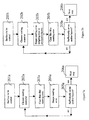
- a preferred embodiment of the invention is a method whereby film-like coating patterns are produced on the surface of the object to be coated (figures 2a and 2b).
- FIGs 2a and 2b there are at least two alternatives, which are illustrated in figures 2a and 2b.
- a common feature for both methods according to this embodiment is that for the surface 201a, 201b to be coated, there is chosen a coating material 202a, 202b. Thereafter, according to figure 2a, the surface of the object in question is coated, 203a, whereafter from the coating there is removed, 204a, those parts of the film that are left over the patterns. Thereafter it is checked, 205a, 205b, whether coating should be continued or not.
- step 206a When a sufficient number of coating layers is achieved, operations proceed to the next step 206a in treating the coated object. If the check-up 205a, 205b reveals that the coating is not yet ready, the coating operation is repeated from step 202a, 202b onwards, until a sufficient number of patterns and/or layers is achieved on the surface, in which case the next step 206a, 206b for treating the coated object can be assumed.
- the method illustrated in figure 2b is essentially similar to the one illustrated in figure 2a. However, the method illustrated in figure 2b differs from the one illustrated in figure 2a as regards both the order and way of realising the design 203b of the surface patterns and the coating 204b.
- the coating 204b there can be used an aligning tray, in which case the forming 204b and shaping 203b of the film-like coating are performed on the object surface at points defined by the tray apertures.
- the shaping 203b of the coating areas has, in a certain sense, taken place prior to the coating 204b proper.
- the patterns created on the surface itself achieve their design 203a simultaneously with the coating 204b, when an aligning tray is used.
- An aligning tray can be a mechanical protection provided with apertures of a desired shape for creating surface patterns on the object to be coated.
- other protective material layers such as lacquers and the like, on the surface of the object to be coated is considered as an aligning tray, when certain spots on the surface to be coated are protected against the influences of the coating method essentially in way that can be compared to the use of a mechanical aligning tray.
- the removal of the extra pieces of film from the coating in order to produce the patterns can be carried out by means of monochromatic and at the same time coherent electromagnetic radiation (various laser applications), by means of electrons and/or other particle radiation as well as chemically, for instance by engraving.
- coherent electromagnetic radiation variable laser applications
- electrons and/or other particle radiation as well as chemically, for instance by engraving.
- the above mentioned ways for producing the patterns can be applied in parallel and/or in series, when a given effect should be produced in a way that is most advantageous for a certain application.
- CVD and PVD processes Chemical Vapour Deposition and Physical Vapour Deposition
- sputtering methods for example electric and/or magnetic fields, which interact with the coating material to be focused and/or with the surface of said object.
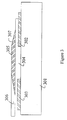
- coatings with suitable refractive indexes for instance coatings 302, 303, 304, 305, 306, 307
- patterns, graphics and/or characters on an optical surface i.e. coating patterns (for example 403a, 403b, 404), for instance on a display (figure 4) and/or on its protective glass sheet 402.
- the surface can be made of glass, plastic or a composite material.
- a person who observes the light reflected from the surface of said object sees how the coated areas are distinguished from their surroundings by a slight contrast and coloured in a way determined by the wavelengths that are left; a typical feature of the way of colouring is that the complementary colours corresponding to colours of the missing wavelengths are emphasised and mixed in other colours.
- the refractive index By means of the refractive index, the reflectance of the surface can be changed, and thus the degree in which the phenomenon stands out from the background can be adjusted.
- a damping interference can also be achieved for most wavelengths.
- Other metal compounds that are suitable with respect to the optical wavelength range can also be used, in which case the film thicknesses vary depending on the desired effect and the refractive index.
- the compounds containing non-metallic materials particularly wear-resistant materials, such as SiO 2 , for example, are suited for coating.
- the layer thickness of the coating materials can also be chosen in a different way, in which case also an interference that intensifies the interference effect can be created.
- the distance travelled by the ray of light in the coating layer is an integral multiple of the wavelength (clause of intensifying interference).
- the clause of attenuating interference prevailing for a given coating layer at a given wavelength can simultaneously be the clause of intensifying interference at another wavelength. This is an important fact with coating layer thicknesses that are larger than the minimum material requirements for coatings, in which case said fact can be utilised in adjusting the colour nuances connected to the created effect.
- the coating layer thicknesses that are feasible from the point of view of the method are within the range of 0.003 ⁇ m - 300 ⁇ m, preferably in range 0.03 - 30 ⁇ m.
- the interference effect can be different in the different coating layers of one and the same object, including as an extreme example of the interference effect a case where the interference phenomenon is not observed at all, for instance when rays of light are reflected from a completely uncoated surface.
- holograms can also be applied in the effect. In that case the thicknesses and materials of the surface layers must be chosen so that as a total effect of the patterns, there is created the three-dimensional space effect typical of holograms.
- figure 4 there is shown, by way of example, a simple draft of a reflection-based pattern design according to the invention, seen on the protective window 402 of the display of a mobile phone 401.
- the pattern design is composed of letters 403a, 403b and 404 from the western alphabet, but the patterns can also be characters of any other alphabet or system, graphic symbols, images or figures.
- a symbol desired by the manufacturer can be marked in a product, on a restricted surface thereof, in order to prove the name and/or authenticity of said product and/or to distinguish a pirate copy from an original product.
- this symbol includes a part belonging to the trade mark identifier desired by the manufacturer, which part may comprise a logo, a graphic symbol, bookmark and/or a combination of these. Because a trade mark identifier or another identifier that has the same position, further on just 'identifier' for short, most advantageously covers just a small portion of the rest of the area to be coated in said product, this embodiment of the invention can be applied in marking nearly any product in order to prove its origins.
- a step for marking the identifier in the appropriate place which may be located in the product package, shell, in a given location in the product itself, in a location of another product to be used in connection with the first product, in a guide instructing the use of said product or in a corresponding literary source, in a certificate of guarantee and/or in a separate certificate of authenticity.
- a step for marking an open identifier in a first identifier location there is included a step for marking an open identifier in a first identifier location, and a protected graphic identifier in another identifier location.
- the open identifier is marked to be visible for the naked eye and can be openly verified without special tools.
- the protected identifier is marked so that it is visible by certain tools, but cannot be directly seen by the naked eye.
- the protected identifier is marked in a sufficiently small size.
- the protected identifier can be detected at another wavelength range of photon radiation than visible light.
- a protected identifier, an open identifier and/or the surroundings of said identifier are self-luminous. In that case the self-luminosity can be achieved by making use of the phosphorescence/fluorescence phenomenon with materials that have said feature as part of their film-like structure.
Landscapes
- Physics & Mathematics (AREA)
- General Physics & Mathematics (AREA)
- Optics & Photonics (AREA)
- Engineering & Computer Science (AREA)
- Computer Networks & Wireless Communication (AREA)
- Signal Processing (AREA)
- Printing Methods (AREA)
- Devices For Indicating Variable Information By Combining Individual Elements (AREA)
- Application Of Or Painting With Fluid Materials (AREA)
Applications Claiming Priority (3)
| Application Number | Priority Date | Filing Date | Title |
|---|---|---|---|
| FI992776 | 1999-12-23 | ||
| FI19992776A FI19992776A7 (fi) | 1999-12-23 | 1999-12-23 | Menetelmä optisen pinnan kuvioimiseksi värisellä heijastuksella |
| US09/746,056 US20020110683A1 (en) | 1999-12-23 | 2000-12-21 | Marking method |
Publications (2)
| Publication Number | Publication Date |
|---|---|
| EP1111409A2 true EP1111409A2 (fr) | 2001-06-27 |
| EP1111409A3 EP1111409A3 (fr) | 2003-11-26 |
Family
ID=26160818
Family Applications (1)
| Application Number | Title | Priority Date | Filing Date |
|---|---|---|---|
| EP00660232A Withdrawn EP1111409A3 (fr) | 1999-12-23 | 2000-12-18 | Méthode de marquage |
Country Status (3)
| Country | Link |
|---|---|
| US (1) | US20020110683A1 (fr) |
| EP (1) | EP1111409A3 (fr) |
| FI (1) | FI19992776A7 (fr) |
Families Citing this family (1)
| Publication number | Priority date | Publication date | Assignee | Title |
|---|---|---|---|---|
| US12166520B2 (en) * | 2021-10-22 | 2024-12-10 | Case-Mate, Inc. | Case with illusory design elements |
Family Cites Families (16)
| Publication number | Priority date | Publication date | Assignee | Title |
|---|---|---|---|---|
| JPS5881976A (ja) * | 1981-11-06 | 1983-05-17 | Toru Mashida | 装飾体の製造法 |
| FR2547775B1 (fr) * | 1983-06-23 | 1987-12-18 | Metalem Sa | Procede de decoration d'un article, application d'un procede de traitement d'un element de silicium, utilisation d'une plaque de silicium traitee et article decore |
| CA1232068A (fr) * | 1984-06-08 | 1988-01-26 | National Research Council Of Canada | Dispositif d'authentification interferometrique a reconnaissance de formes |
| US4694558A (en) * | 1986-01-06 | 1987-09-22 | Gte Products Corporation | Bimetal thermostats and method of manufacture |
| US5360628A (en) * | 1986-04-30 | 1994-11-01 | Butland Trust Organization | Technique for labeling an object for its identification and/or verification |
| EP0330738B1 (fr) * | 1988-03-03 | 1991-11-13 | Landis & Gyr Betriebs AG | Document |
| GB9106128D0 (en) * | 1991-03-22 | 1991-05-08 | Amblehurst Ltd | Article |
| US5296949A (en) * | 1992-04-23 | 1994-03-22 | Flexcon Company Inc. | Optical authentication device |
| US5913543A (en) * | 1992-07-17 | 1999-06-22 | Optical Security Group, Inc. | Tamper evident and counterfeit resisting informational article and associated method |
| US5267756A (en) * | 1992-09-30 | 1993-12-07 | The Upper Deck Company | Authentication system |
| US5549953A (en) * | 1993-04-29 | 1996-08-27 | National Research Council Of Canada | Optical recording media having optically-variable security properties |
| US5510163A (en) * | 1994-05-18 | 1996-04-23 | National Research Council Of Canada | Optical storage media having visible logos |
| DE19727223B4 (de) * | 1997-06-26 | 2005-05-04 | Flabeg Solarglas Gmbh & Co.Kg | Beschichtung zur Beeinflussung des sich durch Reflexion an einer Substratsoberfläche ergebenden spektralen Farbeindrucks |
| US5974150A (en) * | 1997-09-30 | 1999-10-26 | Tracer Detection Technology Corp. | System and method for authentication of goods |
| US5982545A (en) * | 1997-10-17 | 1999-11-09 | Industrial Technology Research Institute | Structure and method for manufacturing surface relief diffractive optical elements |
| US6749123B2 (en) * | 1999-09-07 | 2004-06-15 | American Express Travel Related Services Company, Inc. | Transaction card |
-
1999
- 1999-12-23 FI FI19992776A patent/FI19992776A7/fi unknown
-
2000
- 2000-12-18 EP EP00660232A patent/EP1111409A3/fr not_active Withdrawn
- 2000-12-21 US US09/746,056 patent/US20020110683A1/en not_active Abandoned
Also Published As
| Publication number | Publication date |
|---|---|
| FI19992776L (fi) | 2001-06-24 |
| FI19992776A7 (fi) | 2001-06-24 |
| EP1111409A3 (fr) | 2003-11-26 |
| US20020110683A1 (en) | 2002-08-15 |
Similar Documents
| Publication | Publication Date | Title |
|---|---|---|
| US5009486A (en) | Form depicting, optical interference authenticating device | |
| KR100441995B1 (ko) | 시변각안료를함유하는쌍을이룬시변각장치 | |
| RU2670078C1 (ru) | Оптический компонент для защиты от подделок и изделие с оптической защитой от подделок | |
| US9415622B2 (en) | Security element with optically variable element | |
| US10155408B2 (en) | Optical anti-counterfeiting element, product using same and preparation method therefor | |
| US20180281502A1 (en) | Optical anti-counterfeiting element and optical anti-counterfeiting product utilizing the same | |
| JP6956909B2 (ja) | 光学積層体および物品 | |
| DE102019001193A1 (de) | Transparentes Substrat mit lichtabschirmender Schicht | |
| US10120202B2 (en) | Patterned articles and methods for coating substrates with a patterned layer | |
| JP2009078458A (ja) | 干渉色膜を有する機器用筐体及び機器用装飾体 | |
| CN101011916A (zh) | 具有增强防伪特性的图案光学结构 | |
| US5892600A (en) | Spectacle lens structure with a planar reflective outer surface | |
| JPWO2019124322A1 (ja) | 表示体及び表示体の製造方法 | |
| Zhang et al. | Research on a surface-relief optical waveguide augmented reality display device | |
| WO2017181442A1 (fr) | Élément anti-contrefaçon optique et produit anti-contrefaçon optique | |
| EA039835B1 (ru) | Оптические защитные элементы, маркированный объект, способ аутентификации объекта и применение оптических защитных элементов для аутентификации или защиты от подделки | |
| KR20190141621A (ko) | 멀티 칼라 절연 코팅 및 uv 잉크젯 프린팅 | |
| EP1111409A2 (fr) | Méthode de marquage | |
| AU2021218474B2 (en) | An optical effect device | |
| DE10359156A1 (de) | Anzeigevorrichtung | |
| KR20230043212A (ko) | 광학 적층체 및 물품 | |
| US7940463B2 (en) | Fabricating and using hidden features in an image | |
| US20240140125A1 (en) | Method for producing a security element comprising micro-imaging elements | |
| CN111836727A (zh) | 安全元件、数据载体和方法 | |
| CN112606588A (zh) | 一种光学变色烫金材料 |
Legal Events
| Date | Code | Title | Description |
|---|---|---|---|
| PUAI | Public reference made under article 153(3) epc to a published international application that has entered the european phase |
Free format text: ORIGINAL CODE: 0009012 |
|
| AK | Designated contracting states |
Kind code of ref document: A2 Designated state(s): AT BE CH CY DE DK ES FI FR GB GR IE IT LI LU MC NL PT SE TR |
|
| AX | Request for extension of the european patent |
Free format text: AL;LT;LV;MK;RO;SI |
|
| RAP1 | Party data changed (applicant data changed or rights of an application transferred) |
Owner name: NOKIA CORPORATION |
|
| PUAL | Search report despatched |
Free format text: ORIGINAL CODE: 0009013 |
|
| AK | Designated contracting states |
Kind code of ref document: A3 Designated state(s): AT BE CH CY DE DK ES FI FR GB GR IE IT LI LU MC NL PT SE TR |
|
| AX | Request for extension of the european patent |
Extension state: AL LT LV MK RO SI |
|
| RIC1 | Information provided on ipc code assigned before grant |
Ipc: 7B 42D 15/00 B Ipc: 7G 02B 5/28 B Ipc: 7G 02B 1/10 A |
|
| 17P | Request for examination filed |
Effective date: 20040514 |
|
| AKX | Designation fees paid |
Designated state(s): AT BE CH CY DE DK ES FI FR GB GR IE IT LI LU MC NL PT SE TR |
|
| 17Q | First examination report despatched |
Effective date: 20041029 |
|
| STAA | Information on the status of an ep patent application or granted ep patent |
Free format text: STATUS: THE APPLICATION IS DEEMED TO BE WITHDRAWN |
|
| 18D | Application deemed to be withdrawn |
Effective date: 20050510 |