EP1111763A2 - Gleichstrom/Gleichstrom Umwandler und Verfahren zum Betrieb eines Gleichstrom/Gleichstrom Umwandlers - Google Patents
Gleichstrom/Gleichstrom Umwandler und Verfahren zum Betrieb eines Gleichstrom/Gleichstrom Umwandlers Download PDFInfo
- Publication number
- EP1111763A2 EP1111763A2 EP00127234A EP00127234A EP1111763A2 EP 1111763 A2 EP1111763 A2 EP 1111763A2 EP 00127234 A EP00127234 A EP 00127234A EP 00127234 A EP00127234 A EP 00127234A EP 1111763 A2 EP1111763 A2 EP 1111763A2
- Authority
- EP
- European Patent Office
- Prior art keywords
- charge pump
- voltage
- converter
- output
- pump circuit
- Prior art date
- Legal status (The legal status is an assumption and is not a legal conclusion. Google has not performed a legal analysis and makes no representation as to the accuracy of the status listed.)
- Granted
Links
Images

Classifications
-
- H—ELECTRICITY
- H02—GENERATION; CONVERSION OR DISTRIBUTION OF ELECTRIC POWER
- H02M—APPARATUS FOR CONVERSION BETWEEN AC AND AC, BETWEEN AC AND DC, OR BETWEEN DC AND DC, AND FOR USE WITH MAINS OR SIMILAR POWER SUPPLY SYSTEMS; CONVERSION OF DC OR AC INPUT POWER INTO SURGE OUTPUT POWER; CONTROL OR REGULATION THEREOF
- H02M3/00—Conversion of DC power input into DC power output
- H02M3/02—Conversion of DC power input into DC power output without intermediate conversion into AC
- H02M3/04—Conversion of DC power input into DC power output without intermediate conversion into AC by static converters
- H02M3/06—Conversion of DC power input into DC power output without intermediate conversion into AC by static converters using resistors or capacitors, e.g. potential divider
- H02M3/07—Conversion of DC power input into DC power output without intermediate conversion into AC by static converters using resistors or capacitors, e.g. potential divider using capacitors charged and discharged alternately by semiconductor devices with control electrode, e.g. charge pumps
- H02M3/073—Charge pumps of the Schenkel-type
-
- H—ELECTRICITY
- H02—GENERATION; CONVERSION OR DISTRIBUTION OF ELECTRIC POWER
- H02M—APPARATUS FOR CONVERSION BETWEEN AC AND AC, BETWEEN AC AND DC, OR BETWEEN DC AND DC, AND FOR USE WITH MAINS OR SIMILAR POWER SUPPLY SYSTEMS; CONVERSION OF DC OR AC INPUT POWER INTO SURGE OUTPUT POWER; CONTROL OR REGULATION THEREOF
- H02M1/00—Details of apparatus for conversion
- H02M1/14—Arrangements for reducing ripples from DC input or output
- H02M1/146—Arrangements for reducing ripples from DC input or output using discharge tubes
-
- H—ELECTRICITY
- H02—GENERATION; CONVERSION OR DISTRIBUTION OF ELECTRIC POWER
- H02M—APPARATUS FOR CONVERSION BETWEEN AC AND AC, BETWEEN AC AND DC, OR BETWEEN DC AND DC, AND FOR USE WITH MAINS OR SIMILAR POWER SUPPLY SYSTEMS; CONVERSION OF DC OR AC INPUT POWER INTO SURGE OUTPUT POWER; CONTROL OR REGULATION THEREOF
- H02M1/00—Details of apparatus for conversion
- H02M1/0003—Details of control, feedback or regulation circuits
- H02M1/0025—Arrangements for modifying reference values, feedback values or error values in the control loop of a converter
-
- H—ELECTRICITY
- H02—GENERATION; CONVERSION OR DISTRIBUTION OF ELECTRIC POWER
- H02M—APPARATUS FOR CONVERSION BETWEEN AC AND AC, BETWEEN AC AND DC, OR BETWEEN DC AND DC, AND FOR USE WITH MAINS OR SIMILAR POWER SUPPLY SYSTEMS; CONVERSION OF DC OR AC INPUT POWER INTO SURGE OUTPUT POWER; CONTROL OR REGULATION THEREOF
- H02M1/00—Details of apparatus for conversion
- H02M1/0003—Details of control, feedback or regulation circuits
- H02M1/0032—Control circuits allowing low power mode operation, e.g. in standby mode
-
- Y—GENERAL TAGGING OF NEW TECHNOLOGICAL DEVELOPMENTS; GENERAL TAGGING OF CROSS-SECTIONAL TECHNOLOGIES SPANNING OVER SEVERAL SECTIONS OF THE IPC; TECHNICAL SUBJECTS COVERED BY FORMER USPC CROSS-REFERENCE ART COLLECTIONS [XRACs] AND DIGESTS
- Y02—TECHNOLOGIES OR APPLICATIONS FOR MITIGATION OR ADAPTATION AGAINST CLIMATE CHANGE
- Y02B—CLIMATE CHANGE MITIGATION TECHNOLOGIES RELATED TO BUILDINGS, e.g. HOUSING, HOUSE APPLIANCES OR RELATED END-USER APPLICATIONS
- Y02B70/00—Technologies for an efficient end-user side electric power management and consumption
- Y02B70/10—Technologies improving the efficiency by using switched-mode power supplies [SMPS], i.e. efficient power electronics conversion e.g. power factor correction or reduction of losses in power supplies or efficient standby modes
Definitions
- the invention relates to a DC/DC converter including a charge pump circuit and a method of operating one such DC/DC converter.
- Horowitz also describes a simple DC/DC converter operating on the charge pump principle with which an output voltage corresponding maximally to roughly twice the input voltage is achievable.
- the basic circuit of the converter consists substantially of a charge pump capacitor and four controllable switches (e.g. MOSFETs) whereby one electrode of the charge pump capacitor is connectable via a first switch to the input voltage terminal of the converter and via a second switch to GND, and the other electrode of the capacitor is connectable via the third switch to the input voltage terminal and via the fourth switch to the output voltage terminal of the converter.
- MOSFETs controllable switches
- the converter comprises furthermore a control circuit including a clock which clocks the switches so that in a first phase of a clock cycle, the so-called charging phase, the second switch and the third switch are ON whilst the other switches are OFF, so that the charge pump capacitor is charged to the input voltage, and in the second phase of a clock cycle, the so-called discharge phase, the first switch and the fourth switch are ON whilst the other switches are OFF, so that then the charged charge pump capacitor is connected in series to the input voltage which outputs a voltage value to the smoothing and storage capacitor located at the output of the circuit, this voltage value corresponding to roughly twice the input voltage.
- a control circuit including a clock which clocks the switches so that in a first phase of a clock cycle, the so-called charging phase, the second switch and the third switch are ON whilst the other switches are OFF, so that the charge pump capacitor is charged to the input voltage, and in the second phase of a clock cycle, the so-called discharge phase, the first switch and the fourth switch are ON whilst
- charge pumps are conceivable which produce an optimum multiple of the input voltage, which invert or reduce the input voltage.
- DC/DC converter regulators comprise as a rule a comparator which compares the actual output voltage or a voltage proportional to the actual output voltage (which may be derived from the output voltage e.g. across a voltage divider) to a defined reference voltage representing the design output voltage, and then when a deviation is sensed, outputs a control signal, with the aid of which the actual output voltage is adapted to the defined design output voltage value.
- the control signal of the comparator changes, e.g. via a gate of one of the MOSFET switches, the ON resistance of the MOSFET so that the drop in voltage across the switch is increased or decreased resulting in a reduction or increase in the actual output voltage of the converter.
- the linear regulator has, however, the disadvantage that the energy losses resulting from switching the switches of the charge pump are relatively high since the charge pump is always in operation in the case of the linear regulator. These energy losses result from the currents required to charge the gates of the MOS power transistors at a constant frequency even when no current flows at the output of the converter.
- the skip-mode regulator which makes use of the control signal of the comparator to cycle the charge pump ON/OFF depending on the output current requirement and the resulting actual output voltage of the DC/DC converter so that a charge is pumped to the smoothing and storage capacitor located at the output of the circuit only if the voltage across the capacitor has dropped below the design output voltage level.
- the skip-mode regulator thus operates particularly energy-saving and is particularly suitable for applications in which small load currents alternate with large load currents, i.e. it guaranteeing a minor quiescent current of the converter.
- the disadvantage of the skip-mode regulator is, however, that the ON/OFF switching times of the charge pump depend on the average output current in each case to be furnished by the DC/DC converter, i.e. the frequency spectrum resulting at the output of the converter is totally undefined. In addition to this the ripple of the output voltage is relatively heavy since the flow of output current is not continual in the skip-mode regulator.
- the object of the present invention is thus to provide a DC/DC converter operating on the charge pump principle which is superior to the DC/DC converters regulated hitherto either by the skip mode or linear regulator principle and obviates the disadvantages as described above at least in part.
- the intention is to provide a corresponding method of operating a DC/DC converter which is superior to the method hitherto.
- a DC/DC converter including a charge pump circuit comprising:
- the DC/DC converter in accordance with the invention makes clever use of the advantages afforded by the two differingly regulated converters by it being skip-mode regulated when the converter output current is low and linearly regulated when the converter output current is higher, selecting the one or other regulating mode being done automatically and simply achievable.
- the DC/DC converter in accordance with the invention comprises both a high efficiency at low output currents and a defined output frequency spectrum at high output currents.
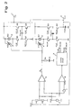
- Fig.1 there is illustrated a circuit diagram of a first embodiment of the DC/DC converter in accordance with the invention, the configuration of which will first be described.
- the DC/DC converter in accordance with the invention as shown in Fig. 1 comprises substantially a charge pump circuit and a regulator circuit which regulates the output voltage of the DC/DC converter to a design value.
- the charge pump circuit comprises a charge pump capacitor Cpump and four controllable switches S1, S2, S3, S4 preferably consisting of MOSFETs as shown in Fig. 1.
- the one electrode of the charge pump capacitor Cpump is connectable via a first controllable switch S1 to the input 1 of the DC/DC converter and via the second controllable switch S2 to GND, and the other electrode of the charge pump capacitor Cpump is connectable via the third controllable switch S3 to the input 1 of the DC/DC converter and via the fourth controllable switch to the output 2 of the DC/DC converter.
- the charge pump circuit comprises in addition a first current source 3 located between the input 1 of the DC/DC converter and the first controllable switch S1 and furnishing a predetermined and constant basic current Ib, and a second current source 4 connected in parallel to the first current source 3 and furnishing an additional current Ir, the amperage of which is controllable.
- a storage capacitor Cout Located at the output 2 of the DC/DC converter, as is usual for DC/DC converters, is a storage capacitor Cout.
- the output voltage regulator circuit comprises an operational amplifier 5 receiving at its non-inverting input a reference voltage Vref which e.g. may originate from a reference voltage generator circuit (not shown in detail). At its inverting input the operational amplifier receives a voltage proportional to the output voltage Vout of the DC/DC converter, this proportional voltage being tapped from the resistor R2 of the voltage divider comprising the two resistors R1 and R2 at which the output voltage Vout of the DC/DC converter is connected.
- the operational amplifier 5 is a so-called transconductance amplifier (VC-OPV) and furnishes at its output a current Ic as a function of the difference between the voltages applied to its inputs.
- the comparator 6 outputs a control signal to the control circuit 8 which has one of two possible output statuses; a first output status when the voltage characterizing the output voltage is smaller than the reference voltage Voff, and a second output status when the voltage characterizing the output voltage is larger than the second reference voltage Voff.
- the control circuit 8 which serves to control the controllable switches S1, S2, S3 and S4 of the charge pump circuit comprises conventionally as the central element a clock from which the signals "CLK” and “NCLK” are derived which are applied to the gates of the controllable switches S2, S3 or S1, S4.
- the "CLK” signal is opposite in phase to that of the "NCLK” signal.
- the charge pump circuit comprising the charge pump capacitor Cpump and four controllable switches S1, S2, S3, S4 cooperates with the control circuit 8 conventionally, i.e. the MOSFETs S2, S3 and MOSFETs S1, S4 are cycled ON by the clock signals "CLK” and "NCLK” so that the corresponding other MOSFETs in each case are OFF.
- the current flowing in the discharge phase representing the output current of the DC/DC converter is dictated by the sum of the currents from the first current source 3 and the controllable second current source 4.
- Iout (Ir + Ib) /2
- Ib is the constant basic current furnished by the first current source 3
- Ir is the controllable current furnished by the second current source 4.
- the factor 1/2 results from the fact that the charge pump circuit furnishes a current only during the discharge phase (assuming that charging and discharge phase are equally long).
- the operational amplifier 5 in conjunction with the RC compensation pad Rk, Ck and the controllable second current source 4.
- the "linear regulation mechanism" as described above signals the second current source 4 OFF so completely that no current Ir flows any more at all, i.e. any further regulation of the output voltage Vout with a further drop in the average output current then no longer being possible by the operational amplifier 5 and the RC pad Rk, Ck.
- the comparator 6 - now operating on the skip-mode principle - handles regulation of the output voltage Vout of the DC/DC converter, by a control signal having the first status (e.g. HI) being output to the control circuit 8 advising it that it is now required to deactivate the charge pump circuit 8 (the control signal output by the comparator 6 then assuming the above-mentioned second status (e.g.
- the control circuit 8 then deactivates the charge pump circuit (e.g. by deactivating the clock) as a result of which the output capacitor Cout no longer receives a charge for some time and the output voltage Vout across the output capacitor Cout descreases until at some point in time it drops below the value of the second reference voltage Voff.
- the comparator 6 then outputs the second control signal to the control circuit 8 as a result of which it activates the charge pump circuit 8 by it again commencing to cycle the MOSFETs S1, S4 and S2, S3 ON/OFF respectively in the manner as described above.
- the DC/DC converter in accordance with the invention has a number of advantages.
- the output currents of the DC/DC converter are larger on an average, at which it operates in the linear regulation mode, it furnishes a defined frequency spectrum due to the known switching frequency of the control circuit clock.
- the output currents of the DC/DC converter are smaller on an average, at which it operates in the skip-mode, it has a high efficiency since the charge pump circuit is only activated when energy is actually required at the output.
- the ripple of the output voltage in the skip-mode is greatly reduced. In this arrangement the output voltage ripple in the skip-mode is limited by the output current peaks limited by the predetermined constant basic current Ib.
- the basic current Ib furished during skip-mode regulation is precisely defined thus assuring that the selection between the two regulation modes is always made at the same output current.
- the maximum output current of the charge pump circuit is limited by the arrangement of the two current sources to a value of (Ib+ Irmax)/2.
- Fig. 2 there is illustrated a circuit diagram of a second embodiment of the DC/DC converter in accordance with the invention.
- the second charge pump circuit comprising the charge pump capacitor Cpump2 and the four switches S5, S6, S7, S8 is connected in parallel to the first charge pump circuit, it being controlled by the control circuit 8 opposite in phase to the first charge pump circuit, so that when the first charge pump circuit (Cpumpl, S1-S4) is in the discharge phase (S1, S4 ON; S2, S3 OFF) then the second charge pump circuit (Cpump2, S5-S8) is in the charge phase (S6, S7 ON; S5, S8 OFF) and vice-versa.
- the opposite phase control is evident in Fig. 2 from the differing distribution of the two switching signals "CLK" and "NCLK" at the gates of the MOSFETs of the two charge pump circuits.
- the various embodiments of the DC/DC converter in accordance with the invention are fabricated preferably in the form of an integrated circuit.
- the circuit may be simplified also so that the MOSFETs are made use of as the first and second current source (3, 4 and 10, 11 resp.) as already provided in the discharge path, via which current flows in the discharge phase of the charge pump circuit to the output of the DC/DC converter, as controllable switches of the charge pump circuit.
- the MOSFETs S1, S4, S5 or S8 may be used as current sources which, when the circuit is fabricated integrated, results in a reduction in the chip surface area required.
- the two current sources may be arranged e.g. in the charge pump circuit at a location other than that as shown in in the embodiments, e.g. in the charging path of the charge pump circuit via which in the charging phase of the charge pump circuit the charge pump capacitor(s) is/are charged.
- the circuit may, of course, comprise several charge pump capacitors and more or fewer controllable switches than is the case in the selected embodiments - this is still within the gist of the invention, the same as in making use of charge pump circuits which increase, invert or reduce the input voltage of the DC/DC converter.
Landscapes
- Engineering & Computer Science (AREA)
- Power Engineering (AREA)
- Dc-Dc Converters (AREA)
- Input Circuits Of Receivers And Coupling Of Receivers And Audio Equipment (AREA)
Applications Claiming Priority (2)
| Application Number | Priority Date | Filing Date | Title |
|---|---|---|---|
| DE19962523A DE19962523A1 (de) | 1999-12-23 | 1999-12-23 | Gleichspannungswandler und Verfahren zum Betreiben eines Gleichspannungswandlers |
| DE19962523 | 1999-12-23 |
Publications (3)
| Publication Number | Publication Date |
|---|---|
| EP1111763A2 true EP1111763A2 (de) | 2001-06-27 |
| EP1111763A3 EP1111763A3 (de) | 2002-01-09 |
| EP1111763B1 EP1111763B1 (de) | 2003-06-11 |
Family
ID=7934167
Family Applications (1)
| Application Number | Title | Priority Date | Filing Date |
|---|---|---|---|
| EP00127234A Expired - Lifetime EP1111763B1 (de) | 1999-12-23 | 2000-12-15 | Gleichstrom/Gleichstrom Umwandler und Verfahren zum Betrieb eines Gleichstrom/Gleichstrom Umwandlers |
Country Status (6)
| Country | Link |
|---|---|
| US (1) | US6392904B1 (de) |
| EP (1) | EP1111763B1 (de) |
| JP (1) | JP2001211636A (de) |
| AT (1) | ATE242931T1 (de) |
| DE (2) | DE19962523A1 (de) |
| TW (1) | TW533662B (de) |
Cited By (10)
| Publication number | Priority date | Publication date | Assignee | Title |
|---|---|---|---|---|
| EP1310959A1 (de) * | 2001-11-09 | 2003-05-14 | STMicroelectronics S.r.l. | Ladungspumpeschaltung mit niedriger Leistung |
| WO2004062074A3 (en) * | 2002-12-23 | 2004-11-04 | Sandisk Corp | High voltage ripple reduction and substrate protection |
| NL1027565C2 (nl) * | 2003-11-24 | 2006-11-14 | Samsung Electronics Co Ltd | Toestel en werkwijze voor stabiliseren van een versterkte spanning, toestel en werkwijze voor opwekken van een versterkte spanning daarmee. |
| US7145381B2 (en) | 2003-08-12 | 2006-12-05 | Samsung Electronics Co., Ltd. | Apparatus for controlling a boosted voltage and method of controlling a boosted voltage |
| US7778055B2 (en) | 2005-03-18 | 2010-08-17 | Austriamicrosystems Ag | Voltage converter |
| CN101286693B (zh) * | 2007-04-10 | 2011-03-30 | 立锜科技股份有限公司 | 电荷泵调节器及产生一受调节的电压的方法 |
| EP2665171A1 (de) * | 2012-05-14 | 2013-11-20 | austriamicrosystems AG | Ladepumpenschaltung und Verfahren zur Erzeugung einer Versorgungsspannung |
| EP2712072A1 (de) * | 2012-09-21 | 2014-03-26 | Nxp B.V. | Ausgangsoberwellenspannungsteuerung für einen kapazitiven Gleichspannungswandler |
| EP2884642A1 (de) * | 2013-12-11 | 2015-06-17 | Nxp B.V. | Gleichstrom-Gleichstromspannungswandler und -wandlungsverfahren |
| CN114285267A (zh) * | 2020-12-21 | 2022-04-05 | 马东林 | 一种可组合电荷泵及其控制方法 |
Families Citing this family (41)
| Publication number | Priority date | Publication date | Assignee | Title |
|---|---|---|---|---|
| GB2330679B (en) * | 1997-10-21 | 2002-04-24 | 911 Emergency Products Inc | Warning signal light |
| US7142040B2 (en) * | 2003-03-27 | 2006-11-28 | Device Engineering Co., Ltd. | Stabilized power supply circuit |
| JP2005151777A (ja) * | 2003-11-19 | 2005-06-09 | Sanyo Electric Co Ltd | チャージポンプ回路およびアンプ |
| US7190210B2 (en) * | 2004-03-25 | 2007-03-13 | Integral Wave Technologies, Inc. | Switched-capacitor power supply system and method |
| US7239194B2 (en) * | 2004-03-25 | 2007-07-03 | Integral Wave Technologies, Inc. | Trench capacitor power supply system and method |
| US7034602B2 (en) * | 2004-03-29 | 2006-04-25 | Semiconductor Components Industries, L.L.C. | Method of forming a floating charge pump and structure therefor |
| ITVA20040026A1 (it) * | 2004-06-25 | 2004-09-25 | St Microelectronics Srl | Metodo di controllo di un generatore a pompa di carica e relativo generatore a pompa di carica |
| TWI261406B (en) * | 2004-07-08 | 2006-09-01 | Analog Integrations Corp | Charge pump DC/DC converter with constant-frequency operation |
| ITVA20040029A1 (it) * | 2004-07-15 | 2004-10-15 | St Microelectronics Srl | Generatore a pompa di carica e relativo metodo di controllo |
| EP1635444B1 (de) * | 2004-09-14 | 2009-01-07 | Dialog Semiconductor GmbH | Abschaltvorrichtung für Ladungspumpeschaltung |
| JP4666345B2 (ja) * | 2004-11-05 | 2011-04-06 | ローム株式会社 | チャージポンプ回路 |
| WO2006061952A1 (ja) * | 2004-12-06 | 2006-06-15 | Rohm Co., Ltd | 昇圧回路及びこれを用いた携帯機器 |
| CN101095276B (zh) * | 2005-01-14 | 2011-09-07 | 半导体元件工业有限责任公司 | 直流-直流转换器及其方法 |
| US7375992B2 (en) * | 2005-01-24 | 2008-05-20 | The Hong Kong University Of Science And Technology | Switched-capacitor regulators |
| US7430133B1 (en) * | 2005-05-31 | 2008-09-30 | National Semiconductor Corporation | Apparatus and method for switch connected as a diode in a charge pump |
| JP4689394B2 (ja) * | 2005-07-29 | 2011-05-25 | パナソニック株式会社 | 半導体集積回路 |
| US7190598B1 (en) * | 2005-09-02 | 2007-03-13 | Texas Instruments Incorporated | Three-phase low noise charge pump and method |
| JP2007089242A (ja) * | 2005-09-20 | 2007-04-05 | Seiko Instruments Inc | チャージポンプ式昇圧回路を有する半導体装置 |
| JP2008017596A (ja) * | 2006-07-05 | 2008-01-24 | Matsushita Electric Ind Co Ltd | 半導体集積回路 |
| JP2008029098A (ja) * | 2006-07-20 | 2008-02-07 | Oki Electric Ind Co Ltd | 昇圧回路 |
| JP4912067B2 (ja) * | 2006-07-27 | 2012-04-04 | ローム株式会社 | 半導体集積回路およびそれを備えた電子機器 |
| WO2008027038A1 (en) * | 2006-08-28 | 2008-03-06 | Semiconductor Components Industries, L.L.C. | Charge pump controller and method therefor |
| US7898234B1 (en) * | 2006-08-30 | 2011-03-01 | Dell Products, Lp | Device and method for rapid voltage ramp-up to regulator target voltage |
| DE102006046387B4 (de) * | 2006-09-29 | 2015-11-19 | Texas Instruments Deutschland Gmbh | DC-DC-Aufwärtswandler mit einer Ladungspumpe |
| JP5078464B2 (ja) * | 2007-06-29 | 2012-11-21 | 株式会社リコー | チャージポンプ回路 |
| JP4682173B2 (ja) * | 2007-07-12 | 2011-05-11 | 株式会社日立製作所 | 電圧駆動型半導体素子のドライブ回路及びインバータ装置 |
| US7884594B2 (en) * | 2008-07-31 | 2011-02-08 | International Business Machines Corporation | Method and apparatus for distribution of a voltage reference in integrated circuits |
| JP2011061891A (ja) * | 2009-09-07 | 2011-03-24 | Renesas Electronics Corp | 負荷駆動回路 |
| CN102111068A (zh) * | 2009-12-24 | 2011-06-29 | 上海华虹Nec电子有限公司 | 电荷泵电路的结构及电荷泵的启动方法 |
| US8319545B2 (en) * | 2010-02-24 | 2012-11-27 | Linear Technology Corporation | Charge pump with reduced current variation |
| JP5491969B2 (ja) * | 2010-05-31 | 2014-05-14 | ローム株式会社 | トランスミッタ、インタフェイス装置、車載通信システム |
| DE102011086309A1 (de) * | 2011-11-14 | 2013-05-16 | Continental Automotive Gmbh | Schaltungsanordnung mit gegenphasig arbeitenden Ladungspumpen zum Aufladen eines elektrischen Energiespeichers |
| TWI508420B (zh) * | 2013-03-15 | 2015-11-11 | Silicon Motion Inc | 應用於高負載電流之電荷注入式開關電容穩壓器 |
| US9071137B2 (en) * | 2013-04-10 | 2015-06-30 | Himax Analogic, Inc. | Driving circuit and error amplifier thereof |
| CN104143907B (zh) * | 2014-08-15 | 2017-10-31 | 中国科学院微电子研究所 | 非连续性电流控制的双环电荷泵控制电路 |
| US9595871B1 (en) | 2015-12-21 | 2017-03-14 | Texas Instruments Deutschland Gmbh | High efficiency inductive capacitive DC-DC converter |
| CN110622403B (zh) * | 2017-05-09 | 2023-01-10 | 索尼半导体解决方案公司 | 电源电路 |
| US11323026B2 (en) * | 2019-09-06 | 2022-05-03 | Intel Corporation | Hybrid digital linear and switched capacitor voltage regulator |
| CN112511000B (zh) * | 2019-09-16 | 2025-01-10 | 微芯片技术股份有限公司 | 具有滞后控制的电压转换器 |
| EP3826183B1 (de) * | 2019-11-21 | 2023-06-21 | Murata Manufacturing Co., Ltd. | Ladungspumpenschaltung und verfahren zur hochspannungserzeugung mit verbesserter psrr |
| EP4216419B1 (de) | 2022-01-21 | 2024-10-09 | Socionext Inc. | Geschaltete stromquellenschaltungen |
Family Cites Families (9)
| Publication number | Priority date | Publication date | Assignee | Title |
|---|---|---|---|---|
| DE69430806T2 (de) * | 1994-12-05 | 2002-12-12 | Stmicroelectronics S.R.L., Agrate Brianza | Ladungspumpe-Spannungsvervielfacherschaltung mit Regelungsrückkopplung und Verfahren dafür |
| US5680300A (en) * | 1995-12-22 | 1997-10-21 | Analog Devices, Inc. | Regulated charge pump DC/DC converter |
| US5672952A (en) * | 1996-07-01 | 1997-09-30 | Analog Devices, Inc. | Controller for battery charger with reduced reverse leakage current |
| JP3884810B2 (ja) * | 1997-01-21 | 2007-02-21 | 株式会社ルネサステクノロジ | 高電圧発生装置 |
| KR100273278B1 (ko) * | 1998-02-11 | 2001-01-15 | 김영환 | 반도체 소자의 펌핑회로 |
| US6229385B1 (en) * | 1999-01-29 | 2001-05-08 | Linear Technology Corporation | Control feature for IC without using a dedicated pin |
| US6242970B1 (en) * | 1999-09-04 | 2001-06-05 | Texas Instruments Incorporated | Charge-pump device and method of sequencing charge-pump switches |
| US6201717B1 (en) * | 1999-09-04 | 2001-03-13 | Texas Instruments Incorporated | Charge-pump closely coupled to switching converter |
| US6172493B1 (en) * | 1999-09-04 | 2001-01-09 | Texas Instruments Incorporated | Switch-mode power converter circuit |
-
1999
- 1999-12-23 DE DE19962523A patent/DE19962523A1/de not_active Withdrawn
-
2000
- 2000-12-15 EP EP00127234A patent/EP1111763B1/de not_active Expired - Lifetime
- 2000-12-15 DE DE60003276T patent/DE60003276T2/de not_active Expired - Lifetime
- 2000-12-15 AT AT00127234T patent/ATE242931T1/de not_active IP Right Cessation
- 2000-12-20 US US09/741,951 patent/US6392904B1/en not_active Expired - Lifetime
- 2000-12-22 TW TW089127601A patent/TW533662B/zh not_active IP Right Cessation
- 2000-12-25 JP JP2000393353A patent/JP2001211636A/ja not_active Abandoned
Cited By (16)
| Publication number | Priority date | Publication date | Assignee | Title |
|---|---|---|---|---|
| EP1310959A1 (de) * | 2001-11-09 | 2003-05-14 | STMicroelectronics S.r.l. | Ladungspumpeschaltung mit niedriger Leistung |
| US6816001B2 (en) | 2001-11-09 | 2004-11-09 | Stmicroelectronics S.R.L. | Low power charge pump circuit |
| WO2004062074A3 (en) * | 2002-12-23 | 2004-11-04 | Sandisk Corp | High voltage ripple reduction and substrate protection |
| US7116155B2 (en) | 2002-12-23 | 2006-10-03 | Sandisk Corporation | High voltage ripple reduction and substrate protection |
| US7145381B2 (en) | 2003-08-12 | 2006-12-05 | Samsung Electronics Co., Ltd. | Apparatus for controlling a boosted voltage and method of controlling a boosted voltage |
| NL1027565C2 (nl) * | 2003-11-24 | 2006-11-14 | Samsung Electronics Co Ltd | Toestel en werkwijze voor stabiliseren van een versterkte spanning, toestel en werkwijze voor opwekken van een versterkte spanning daarmee. |
| US7778055B2 (en) | 2005-03-18 | 2010-08-17 | Austriamicrosystems Ag | Voltage converter |
| CN101286693B (zh) * | 2007-04-10 | 2011-03-30 | 立锜科技股份有限公司 | 电荷泵调节器及产生一受调节的电压的方法 |
| EP2665171A1 (de) * | 2012-05-14 | 2013-11-20 | austriamicrosystems AG | Ladepumpenschaltung und Verfahren zur Erzeugung einer Versorgungsspannung |
| US8860498B2 (en) | 2012-05-14 | 2014-10-14 | Ams Ag | Charge pump circuit and method for generating a supply voltage |
| EP3404815A1 (de) * | 2012-05-14 | 2018-11-21 | ams AG | Ladepumpenschaltung und verfahren zur erzeugung einer referenzspannung |
| EP2712072A1 (de) * | 2012-09-21 | 2014-03-26 | Nxp B.V. | Ausgangsoberwellenspannungsteuerung für einen kapazitiven Gleichspannungswandler |
| US9385591B2 (en) | 2012-09-21 | 2016-07-05 | Nxp B.V. | Output ripple voltage control for a capacitive DC/DC converter |
| EP2884642A1 (de) * | 2013-12-11 | 2015-06-17 | Nxp B.V. | Gleichstrom-Gleichstromspannungswandler und -wandlungsverfahren |
| US9419516B2 (en) | 2013-12-11 | 2016-08-16 | Nxp B.V. | DC-DC voltage converter and conversion method |
| CN114285267A (zh) * | 2020-12-21 | 2022-04-05 | 马东林 | 一种可组合电荷泵及其控制方法 |
Also Published As
| Publication number | Publication date |
|---|---|
| JP2001211636A (ja) | 2001-08-03 |
| DE19962523A1 (de) | 2001-08-02 |
| TW533662B (en) | 2003-05-21 |
| US20020075705A1 (en) | 2002-06-20 |
| EP1111763B1 (de) | 2003-06-11 |
| DE60003276D1 (de) | 2003-07-17 |
| DE60003276T2 (de) | 2004-05-06 |
| US6392904B1 (en) | 2002-05-21 |
| ATE242931T1 (de) | 2003-06-15 |
| EP1111763A3 (de) | 2002-01-09 |
Similar Documents
| Publication | Publication Date | Title |
|---|---|---|
| EP1111763B1 (de) | Gleichstrom/Gleichstrom Umwandler und Verfahren zum Betrieb eines Gleichstrom/Gleichstrom Umwandlers | |
| USRE43414E1 (en) | Synthetic ripple regulator | |
| US7276886B2 (en) | Dual buck-boost converter with single inductor | |
| US8154267B2 (en) | Current mode control type switching regulator | |
| US7116085B2 (en) | DC-DC converter | |
| KR100744592B1 (ko) | Dc-dc 컨버터, dc-dc 컨버터의 제어 회로 및dc-dc 컨버터의 제어 방법 | |
| US8179113B2 (en) | Buck-Boost switching regulator and method thereof for DC/DC conversion | |
| US6438005B1 (en) | High-efficiency, low noise, inductorless step-down DC/DC converter | |
| US7737767B2 (en) | Control circuit and control method for charge pump circuit | |
| US8362755B2 (en) | Current-mode control type DC-DC converter and control method therefor | |
| US20090058507A1 (en) | Bottom Plate Regulated Charge Pump | |
| US20040027104A1 (en) | Multiple output dc-dc converter | |
| EP1067659B1 (de) | Gleichstrom/Gleichstrom Umwandler | |
| US12388349B2 (en) | Adaptive off-time or on-time DC-DC converter | |
| EP1804368A1 (de) | Methode zur Gleichstromwandlung and Gleichstromwandleranordnung | |
| KR20180033178A (ko) | 인덕터 전류에 기반하여 부스트 스위칭 조절기를 제어하기 위한 회로들 및 방법들 | |
| EP4297258B1 (de) | Steuervorrichtung für einen schaltspannungsregler mit verbesserter steuerleistung und steuerverfahren | |
| CN112311236A (zh) | 开关模式电源 | |
| JP2005312169A (ja) | 電圧反転型チャージポンプ回路 | |
| US7952335B2 (en) | Power converter and method for power conversion | |
| EP1594216B1 (de) | Einsatz einer Ladungspumpe mit tätiger Entladefunktion | |
| US7157943B2 (en) | Frequency selection of switch mode power converters via softstart voltage level | |
| US20250317059A1 (en) | Dc/dc converter capable of performing constant on-time control with reduced variations of switching frequency | |
| JPH0624430B2 (ja) | Dc−dcコンバータ |
Legal Events
| Date | Code | Title | Description |
|---|---|---|---|
| PUAI | Public reference made under article 153(3) epc to a published international application that has entered the european phase |
Free format text: ORIGINAL CODE: 0009012 |
|
| AK | Designated contracting states |
Kind code of ref document: A2 Designated state(s): AT BE CH CY DE DK ES FI FR GB GR IE IT LI LU MC NL PT SE TR |
|
| AX | Request for extension of the european patent |
Free format text: AL;LT;LV;MK;RO;SI |
|
| PUAL | Search report despatched |
Free format text: ORIGINAL CODE: 0009013 |
|
| AK | Designated contracting states |
Kind code of ref document: A3 Designated state(s): AT BE CH CY DE DK ES FI FR GB GR IE IT LI LU MC NL PT SE TR |
|
| AX | Request for extension of the european patent |
Free format text: AL;LT;LV;MK;RO;SI |
|
| RIC1 | Information provided on ipc code assigned before grant |
Free format text: 7H 02M 3/00 A, 7H 02M 3/07 B |
|
| 17P | Request for examination filed |
Effective date: 20020709 |
|
| AKX | Designation fees paid |
Free format text: AT BE CH CY DE DK ES FI FR GB GR IE IT LI LU MC NL PT SE TR |
|
| 17Q | First examination report despatched |
Effective date: 20020829 |
|
| GRAH | Despatch of communication of intention to grant a patent |
Free format text: ORIGINAL CODE: EPIDOS IGRA |
|
| GRAH | Despatch of communication of intention to grant a patent |
Free format text: ORIGINAL CODE: EPIDOS IGRA |
|
| GRAA | (expected) grant |
Free format text: ORIGINAL CODE: 0009210 |
|
| AK | Designated contracting states |
Designated state(s): AT BE CH CY DE DK ES FI FR GB GR IE IT LI LU MC NL PT SE TR |
|
| PG25 | Lapsed in a contracting state [announced via postgrant information from national office to epo] |
Ref country code: IT Free format text: LAPSE BECAUSE OF FAILURE TO SUBMIT A TRANSLATION OF THE DESCRIPTION OR TO PAY THE FEE WITHIN THE PRE;WARNING: LAPSES OF ITALIAN PATENTS WITH EFFECTIVE DATE BEFORE 2007 MAY HAVE OCCURRED AT ANY TIME BEFORE 2007. THE CORRECT EFFECTIVE DATE MAY BE DIFFERENT FROM THE ONE RECORDED.SCRIBED TIME-LIMIT Effective date: 20030611 Ref country code: LI Free format text: LAPSE BECAUSE OF FAILURE TO SUBMIT A TRANSLATION OF THE DESCRIPTION OR TO PAY THE FEE WITHIN THE PRESCRIBED TIME-LIMIT Effective date: 20030611 Ref country code: AT Free format text: LAPSE BECAUSE OF FAILURE TO SUBMIT A TRANSLATION OF THE DESCRIPTION OR TO PAY THE FEE WITHIN THE PRESCRIBED TIME-LIMIT Effective date: 20030611 Ref country code: BE Free format text: LAPSE BECAUSE OF FAILURE TO SUBMIT A TRANSLATION OF THE DESCRIPTION OR TO PAY THE FEE WITHIN THE PRESCRIBED TIME-LIMIT Effective date: 20030611 Ref country code: CH Free format text: LAPSE BECAUSE OF FAILURE TO SUBMIT A TRANSLATION OF THE DESCRIPTION OR TO PAY THE FEE WITHIN THE PRESCRIBED TIME-LIMIT Effective date: 20030611 Ref country code: FI Free format text: LAPSE BECAUSE OF FAILURE TO SUBMIT A TRANSLATION OF THE DESCRIPTION OR TO PAY THE FEE WITHIN THE PRESCRIBED TIME-LIMIT Effective date: 20030611 Ref country code: NL Free format text: LAPSE BECAUSE OF FAILURE TO SUBMIT A TRANSLATION OF THE DESCRIPTION OR TO PAY THE FEE WITHIN THE PRESCRIBED TIME-LIMIT Effective date: 20030611 Ref country code: TR Free format text: LAPSE BECAUSE OF FAILURE TO SUBMIT A TRANSLATION OF THE DESCRIPTION OR TO PAY THE FEE WITHIN THE PRESCRIBED TIME-LIMIT Effective date: 20030611 |
|
| REG | Reference to a national code |
Ref country code: GB Ref legal event code: FG4D |
|
| REG | Reference to a national code |
Ref country code: CH Ref legal event code: EP |
|
| REG | Reference to a national code |
Ref country code: IE Ref legal event code: FG4D |
|
| REF | Corresponds to: |
Ref document number: 60003276 Country of ref document: DE Date of ref document: 20030717 Kind code of ref document: P |
|
| PG25 | Lapsed in a contracting state [announced via postgrant information from national office to epo] |
Ref country code: DK Free format text: LAPSE BECAUSE OF FAILURE TO SUBMIT A TRANSLATION OF THE DESCRIPTION OR TO PAY THE FEE WITHIN THE PRESCRIBED TIME-LIMIT Effective date: 20030911 Ref country code: SE Free format text: LAPSE BECAUSE OF FAILURE TO SUBMIT A TRANSLATION OF THE DESCRIPTION OR TO PAY THE FEE WITHIN THE PRESCRIBED TIME-LIMIT Effective date: 20030911 Ref country code: GR Free format text: LAPSE BECAUSE OF FAILURE TO SUBMIT A TRANSLATION OF THE DESCRIPTION OR TO PAY THE FEE WITHIN THE PRESCRIBED TIME-LIMIT Effective date: 20030911 Ref country code: PT Free format text: LAPSE BECAUSE OF FAILURE TO SUBMIT A TRANSLATION OF THE DESCRIPTION OR TO PAY THE FEE WITHIN THE PRESCRIBED TIME-LIMIT Effective date: 20030911 |
|
| PG25 | Lapsed in a contracting state [announced via postgrant information from national office to epo] |
Ref country code: ES Free format text: LAPSE BECAUSE OF FAILURE TO SUBMIT A TRANSLATION OF THE DESCRIPTION OR TO PAY THE FEE WITHIN THE PRESCRIBED TIME-LIMIT Effective date: 20030922 |
|
| NLV1 | Nl: lapsed or annulled due to failure to fulfill the requirements of art. 29p and 29m of the patents act | ||
| PG25 | Lapsed in a contracting state [announced via postgrant information from national office to epo] |
Ref country code: LU Free format text: LAPSE BECAUSE OF NON-PAYMENT OF DUE FEES Effective date: 20031215 Ref country code: IE Free format text: LAPSE BECAUSE OF NON-PAYMENT OF DUE FEES Effective date: 20031215 Ref country code: CY Free format text: LAPSE BECAUSE OF FAILURE TO SUBMIT A TRANSLATION OF THE DESCRIPTION OR TO PAY THE FEE WITHIN THE PRESCRIBED TIME-LIMIT Effective date: 20031215 |
|
| REG | Reference to a national code |
Ref country code: CH Ref legal event code: PL |
|
| PG25 | Lapsed in a contracting state [announced via postgrant information from national office to epo] |
Ref country code: MC Free format text: LAPSE BECAUSE OF NON-PAYMENT OF DUE FEES Effective date: 20031231 |
|
| ET | Fr: translation filed | ||
| PLBE | No opposition filed within time limit |
Free format text: ORIGINAL CODE: 0009261 |
|
| STAA | Information on the status of an ep patent application or granted ep patent |
Free format text: STATUS: NO OPPOSITION FILED WITHIN TIME LIMIT |
|
| 26N | No opposition filed |
Effective date: 20040312 |
|
| REG | Reference to a national code |
Ref country code: IE Ref legal event code: MM4A |
|
| REG | Reference to a national code |
Ref country code: FR Ref legal event code: PLFP Year of fee payment: 16 |
|
| PGFP | Annual fee paid to national office [announced via postgrant information from national office to epo] |
Ref country code: GB Payment date: 20151125 Year of fee payment: 16 |
|
| PGFP | Annual fee paid to national office [announced via postgrant information from national office to epo] |
Ref country code: FR Payment date: 20151124 Year of fee payment: 16 |
|
| PGFP | Annual fee paid to national office [announced via postgrant information from national office to epo] |
Ref country code: DE Payment date: 20151230 Year of fee payment: 16 |
|
| REG | Reference to a national code |
Ref country code: DE Ref legal event code: R119 Ref document number: 60003276 Country of ref document: DE |
|
| GBPC | Gb: european patent ceased through non-payment of renewal fee |
Effective date: 20161215 |
|
| REG | Reference to a national code |
Ref country code: FR Ref legal event code: ST Effective date: 20170831 |
|
| PG25 | Lapsed in a contracting state [announced via postgrant information from national office to epo] |
Ref country code: FR Free format text: LAPSE BECAUSE OF NON-PAYMENT OF DUE FEES Effective date: 20170102 |
|
| PG25 | Lapsed in a contracting state [announced via postgrant information from national office to epo] |
Ref country code: DE Free format text: LAPSE BECAUSE OF NON-PAYMENT OF DUE FEES Effective date: 20170701 Ref country code: GB Free format text: LAPSE BECAUSE OF NON-PAYMENT OF DUE FEES Effective date: 20161215 |