EP1111780A2 - Circuit de filtrage - Google Patents
Circuit de filtrage Download PDFInfo
- Publication number
- EP1111780A2 EP1111780A2 EP00204613A EP00204613A EP1111780A2 EP 1111780 A2 EP1111780 A2 EP 1111780A2 EP 00204613 A EP00204613 A EP 00204613A EP 00204613 A EP00204613 A EP 00204613A EP 1111780 A2 EP1111780 A2 EP 1111780A2
- Authority
- EP
- European Patent Office
- Prior art keywords
- filter
- layer
- electrode
- substrate
- bandpass filter
- Prior art date
- Legal status (The legal status is an assumption and is not a legal conclusion. Google has not performed a legal analysis and makes no representation as to the accuracy of the status listed.)
- Withdrawn
Links
- 239000000758 substrate Substances 0.000 claims abstract description 35
- 239000000919 ceramic Substances 0.000 claims abstract description 5
- 239000003990 capacitor Substances 0.000 claims description 31
- 238000004519 manufacturing process Methods 0.000 claims description 6
- 239000010409 thin film Substances 0.000 claims description 5
- 230000005540 biological transmission Effects 0.000 claims description 3
- 239000011521 glass Substances 0.000 abstract description 17
- 239000000463 material Substances 0.000 abstract description 16
- 229910052710 silicon Inorganic materials 0.000 abstract description 9
- 239000010703 silicon Substances 0.000 abstract description 7
- 239000004020 conductor Substances 0.000 abstract description 3
- XUIMIQQOPSSXEZ-UHFFFAOYSA-N Silicon Chemical compound [Si] XUIMIQQOPSSXEZ-UHFFFAOYSA-N 0.000 abstract 1
- 239000010410 layer Substances 0.000 description 118
- 229910004298 SiO 2 Inorganic materials 0.000 description 35
- 229910052719 titanium Inorganic materials 0.000 description 29
- -1 for example Polymers 0.000 description 14
- 230000001070 adhesive effect Effects 0.000 description 10
- 229910052802 copper Inorganic materials 0.000 description 10
- 239000000853 adhesive Substances 0.000 description 9
- 229910052759 nickel Inorganic materials 0.000 description 9
- 238000001914 filtration Methods 0.000 description 8
- 239000006260 foam Substances 0.000 description 8
- 239000012790 adhesive layer Substances 0.000 description 6
- 229910052797 bismuth Inorganic materials 0.000 description 6
- 229910052804 chromium Inorganic materials 0.000 description 6
- 229910052745 lead Inorganic materials 0.000 description 6
- 238000002161 passivation Methods 0.000 description 6
- 229920003023 plastic Polymers 0.000 description 6
- 239000004033 plastic Substances 0.000 description 6
- 229920000642 polymer Polymers 0.000 description 6
- 229910052708 sodium Inorganic materials 0.000 description 6
- NIXOWILDQLNWCW-UHFFFAOYSA-M Acrylate Chemical compound [O-]C(=O)C=C NIXOWILDQLNWCW-UHFFFAOYSA-M 0.000 description 5
- 229910001218 Gallium arsenide Inorganic materials 0.000 description 5
- 229910010293 ceramic material Inorganic materials 0.000 description 5
- 229910052721 tungsten Inorganic materials 0.000 description 5
- 239000002033 PVDF binder Substances 0.000 description 4
- 229910020684 PbZr Inorganic materials 0.000 description 4
- VYPSYNLAJGMNEJ-UHFFFAOYSA-N Silicium dioxide Chemical compound O=[Si]=O VYPSYNLAJGMNEJ-UHFFFAOYSA-N 0.000 description 4
- 229910052788 barium Inorganic materials 0.000 description 4
- 239000006112 glass ceramic composition Substances 0.000 description 4
- 229910010272 inorganic material Inorganic materials 0.000 description 4
- 239000011147 inorganic material Substances 0.000 description 4
- 229910052741 iridium Inorganic materials 0.000 description 4
- 238000000034 method Methods 0.000 description 4
- 229920001568 phenolic resin Polymers 0.000 description 4
- 229920002981 polyvinylidene fluoride Polymers 0.000 description 4
- 229910052700 potassium Inorganic materials 0.000 description 4
- 239000011241 protective layer Substances 0.000 description 4
- 229910052703 rhodium Inorganic materials 0.000 description 4
- 229910052718 tin Inorganic materials 0.000 description 4
- 229910010413 TiO 2 Inorganic materials 0.000 description 3
- 229910052746 lanthanum Inorganic materials 0.000 description 3
- 229910052748 manganese Inorganic materials 0.000 description 3
- 239000011368 organic material Substances 0.000 description 3
- 229910052594 sapphire Inorganic materials 0.000 description 3
- 239000010980 sapphire Substances 0.000 description 3
- DGXAGETVRDOQFP-UHFFFAOYSA-N 2,6-dihydroxybenzaldehyde Chemical compound OC1=CC=CC(O)=C1C=O DGXAGETVRDOQFP-UHFFFAOYSA-N 0.000 description 2
- 229920001817 Agar Polymers 0.000 description 2
- 229910015902 Bi 2 O 3 Inorganic materials 0.000 description 2
- 241000206672 Gelidium Species 0.000 description 2
- 229910013641 LiNbO 3 Inorganic materials 0.000 description 2
- 229920000877 Melamine resin Polymers 0.000 description 2
- 229910020215 Pb(Mg1/3Nb2/3)O3PbTiO3 Inorganic materials 0.000 description 2
- 239000004642 Polyimide Substances 0.000 description 2
- 239000004743 Polypropylene Substances 0.000 description 2
- 239000004793 Polystyrene Substances 0.000 description 2
- 239000002253 acid Substances 0.000 description 2
- 235000010419 agar Nutrition 0.000 description 2
- DQXBYHZEEUGOBF-UHFFFAOYSA-N but-3-enoic acid;ethene Chemical compound C=C.OC(=O)CC=C DQXBYHZEEUGOBF-UHFFFAOYSA-N 0.000 description 2
- 238000004939 coking Methods 0.000 description 2
- 229920001577 copolymer Polymers 0.000 description 2
- 239000013078 crystal Substances 0.000 description 2
- 238000013016 damping Methods 0.000 description 2
- 238000000151 deposition Methods 0.000 description 2
- 239000003989 dielectric material Substances 0.000 description 2
- KPUWHANPEXNPJT-UHFFFAOYSA-N disiloxane Chemical class [SiH3]O[SiH3] KPUWHANPEXNPJT-UHFFFAOYSA-N 0.000 description 2
- 239000002019 doping agent Substances 0.000 description 2
- 238000005516 engineering process Methods 0.000 description 2
- 229920006332 epoxy adhesive Polymers 0.000 description 2
- 239000005038 ethylene vinyl acetate Substances 0.000 description 2
- IVJISJACKSSFGE-UHFFFAOYSA-N formaldehyde;1,3,5-triazine-2,4,6-triamine Chemical compound O=C.NC1=NC(N)=NC(N)=N1 IVJISJACKSSFGE-UHFFFAOYSA-N 0.000 description 2
- SLGWESQGEUXWJQ-UHFFFAOYSA-N formaldehyde;phenol Chemical compound O=C.OC1=CC=CC=C1 SLGWESQGEUXWJQ-UHFFFAOYSA-N 0.000 description 2
- 239000007849 furan resin Substances 0.000 description 2
- 239000003292 glue Substances 0.000 description 2
- 229920001903 high density polyethylene Polymers 0.000 description 2
- 239000004700 high-density polyethylene Substances 0.000 description 2
- 239000012528 membrane Substances 0.000 description 2
- 239000000203 mixture Substances 0.000 description 2
- 229910052763 palladium Inorganic materials 0.000 description 2
- 229920000090 poly(aryl ether) Polymers 0.000 description 2
- 229920001200 poly(ethylene-vinyl acetate) Polymers 0.000 description 2
- 229920000052 poly(p-xylylene) Polymers 0.000 description 2
- 239000004417 polycarbonate Substances 0.000 description 2
- 229920000515 polycarbonate Polymers 0.000 description 2
- 229920000728 polyester Polymers 0.000 description 2
- 229920001721 polyimide Polymers 0.000 description 2
- 229920001228 polyisocyanate Polymers 0.000 description 2
- 239000005056 polyisocyanate Substances 0.000 description 2
- 229920000582 polyisocyanurate Polymers 0.000 description 2
- 229920001155 polypropylene Polymers 0.000 description 2
- 229920002223 polystyrene Polymers 0.000 description 2
- 229920001343 polytetrafluoroethylene Polymers 0.000 description 2
- 239000004810 polytetrafluoroethylene Substances 0.000 description 2
- 229920002635 polyurethane Polymers 0.000 description 2
- 239000004814 polyurethane Substances 0.000 description 2
- 229920000915 polyvinyl chloride Polymers 0.000 description 2
- 239000004800 polyvinyl chloride Substances 0.000 description 2
- 229920001289 polyvinyl ether Polymers 0.000 description 2
- 239000011148 porous material Substances 0.000 description 2
- 229910052707 ruthenium Inorganic materials 0.000 description 2
- 239000000741 silica gel Substances 0.000 description 2
- 229910002027 silica gel Inorganic materials 0.000 description 2
- 229910052709 silver Inorganic materials 0.000 description 2
- 229910052712 strontium Inorganic materials 0.000 description 2
- 229920003048 styrene butadiene rubber Polymers 0.000 description 2
- 230000001629 suppression Effects 0.000 description 2
- 238000010897 surface acoustic wave method Methods 0.000 description 2
- 229920003002 synthetic resin Polymers 0.000 description 2
- 239000000057 synthetic resin Substances 0.000 description 2
- 229910018072 Al 2 O 3 Inorganic materials 0.000 description 1
- NIXOWILDQLNWCW-UHFFFAOYSA-N acrylic acid group Chemical group C(C=C)(=O)O NIXOWILDQLNWCW-UHFFFAOYSA-N 0.000 description 1
- 239000003522 acrylic cement Substances 0.000 description 1
- 238000006243 chemical reaction Methods 0.000 description 1
- 229910052681 coesite Inorganic materials 0.000 description 1
- 238000010276 construction Methods 0.000 description 1
- 230000008878 coupling Effects 0.000 description 1
- 238000010168 coupling process Methods 0.000 description 1
- 238000005859 coupling reaction Methods 0.000 description 1
- 229910052906 cristobalite Inorganic materials 0.000 description 1
- 238000011161 development Methods 0.000 description 1
- 230000018109 developmental process Effects 0.000 description 1
- 229910003460 diamond Inorganic materials 0.000 description 1
- 239000010432 diamond Substances 0.000 description 1
- 238000005530 etching Methods 0.000 description 1
- 229910052737 gold Inorganic materials 0.000 description 1
- 230000010354 integration Effects 0.000 description 1
- 230000002452 interceptive effect Effects 0.000 description 1
- 229910052749 magnesium Inorganic materials 0.000 description 1
- 125000005395 methacrylic acid group Chemical group 0.000 description 1
- 238000010295 mobile communication Methods 0.000 description 1
- 229910052750 molybdenum Inorganic materials 0.000 description 1
- 239000000178 monomer Substances 0.000 description 1
- 230000003071 parasitic effect Effects 0.000 description 1
- 229910052697 platinum Inorganic materials 0.000 description 1
- 239000000377 silicon dioxide Substances 0.000 description 1
- 235000012239 silicon dioxide Nutrition 0.000 description 1
- 229910052682 stishovite Inorganic materials 0.000 description 1
- 229910052905 tridymite Inorganic materials 0.000 description 1
Images


Classifications
-
- H—ELECTRICITY
- H03—ELECTRONIC CIRCUITRY
- H03H—IMPEDANCE NETWORKS, e.g. RESONANT CIRCUITS; RESONATORS
- H03H9/00—Networks comprising electromechanical or electro-acoustic elements; Electromechanical resonators
- H03H9/46—Filters
- H03H9/54—Filters comprising resonators of piezoelectric or electrostrictive material
- H03H9/58—Multiple crystal filters
- H03H9/60—Electric coupling means therefor
- H03H9/605—Electric coupling means therefor consisting of a ladder configuration
-
- H—ELECTRICITY
- H03—ELECTRONIC CIRCUITRY
- H03H—IMPEDANCE NETWORKS, e.g. RESONANT CIRCUITS; RESONATORS
- H03H3/00—Apparatus or processes specially adapted for the manufacture of impedance networks, resonating circuits, resonators
- H03H3/007—Apparatus or processes specially adapted for the manufacture of impedance networks, resonating circuits, resonators for the manufacture of electromechanical resonators or networks
- H03H3/02—Apparatus or processes specially adapted for the manufacture of impedance networks, resonating circuits, resonators for the manufacture of electromechanical resonators or networks for the manufacture of piezoelectric or electrostrictive resonators or networks
-
- H—ELECTRICITY
- H03—ELECTRONIC CIRCUITRY
- H03H—IMPEDANCE NETWORKS, e.g. RESONANT CIRCUITS; RESONATORS
- H03H9/00—Networks comprising electromechanical or electro-acoustic elements; Electromechanical resonators
- H03H9/02—Details
- H03H9/02007—Details of bulk acoustic wave devices
- H03H9/02086—Means for compensation or elimination of undesirable effects
- H03H9/02094—Means for compensation or elimination of undesirable effects of adherence
-
- H—ELECTRICITY
- H03—ELECTRONIC CIRCUITRY
- H03H—IMPEDANCE NETWORKS, e.g. RESONANT CIRCUITS; RESONATORS
- H03H9/00—Networks comprising electromechanical or electro-acoustic elements; Electromechanical resonators
- H03H9/02—Details
- H03H9/02007—Details of bulk acoustic wave devices
- H03H9/02086—Means for compensation or elimination of undesirable effects
- H03H9/02149—Means for compensation or elimination of undesirable effects of ageing changes of characteristics, e.g. electro-acousto-migration
-
- H—ELECTRICITY
- H03—ELECTRONIC CIRCUITRY
- H03H—IMPEDANCE NETWORKS, e.g. RESONANT CIRCUITS; RESONATORS
- H03H9/00—Networks comprising electromechanical or electro-acoustic elements; Electromechanical resonators
- H03H9/46—Filters
- H03H9/54—Filters comprising resonators of piezoelectric or electrostrictive material
- H03H9/542—Filters comprising resonators of piezoelectric or electrostrictive material including passive elements
-
- H—ELECTRICITY
- H03—ELECTRONIC CIRCUITRY
- H03H—IMPEDANCE NETWORKS, e.g. RESONANT CIRCUITS; RESONATORS
- H03H9/00—Networks comprising electromechanical or electro-acoustic elements; Electromechanical resonators
- H03H9/46—Filters
- H03H9/54—Filters comprising resonators of piezoelectric or electrostrictive material
- H03H9/58—Multiple crystal filters
- H03H9/581—Multiple crystal filters comprising ceramic piezoelectric layers
Definitions
- the invention relates to a filter arrangement. Furthermore, the invention relates to another Transmitter, a receiver and a mobile device with a filter arrangement and a Method of making a filter assembly.
- the filters mentioned, the frequencies outside the Passband lie, not completely, but only suppressed to a certain extent. This can be for certain applications, such as signal filtering in the High frequency part of mobile phones or base stations, may not be sufficient.
- the object of the invention is to provide a filter with a bandpass filter function, which has improved suppression outside the pass band.
- a filter arrangement which has a substrate and thereon applied a bandpass filter and a notch filter, which are coupled together, contains.
- the notch filter is between the input of the bandpass filter and earth or is connected between the output of the bandpass filter and earth.
- the bandpass filter and the notch filter are thin film filters.
- the bandpass filter has a filter arrangement made of resonators contains.
- the filter arrangement bulk wave resonators, surface wave resonators or contains ceramic, electromagnetic resonators.
- Bandpass filters which have a filter arrangement composed of resonators lower losses in the pass band because they have higher Q qualities than, for example, LC filters exhibit.
- bandpass filters made from resonators have a steeper drop at the edge of the passband as comparable LC combinations.
- a bulk wave resonator is a resonator unit and a reflection element which is arranged between the substrate and the resonator unit is contains.
- Such a bulk wave resonator can be easily done using thin film techniques and, above all, be manufactured with a small footprint. Besides, it is one Bulk wave resonators are significantly more robust than other types of bulk wave resonators such as single crystal resonators, resonators with membranes or resonators with an air gap.
- the notch filter has a capacitor and an inductor contains.
- Such a notch filter can be simple, inexpensive using thin-film technology and manufactured with little space on the same substrate as the bandpass filter become.
- the invention also relates to a transmitter, a receiver, a mobile radio device and a wireless data transmission system equipped with a filter arrangement, which a Substrate and a bandpass filter and a notch filter applied to each other are linked.
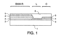
- a filter arrangement with a bandpass filter and a notch filter has a substrate 1, which is, for example, made of a ceramic material, a ceramic material with a planarization layer made of glass, a glass-ceramic material, a glass material, silicon, GaAs or sapphire.
- a passivation layer made of, for example, SiO 2 or glass is also applied.
- a reflection element 2 which is a layer of a sound reflection material from the group of polymeric and porous materials.
- an airgel, a xerogel, a glass foam, a foam-like adhesive, a foam or a plastic with a low density can be used as the sound reflection material.
- An inorganic airgel made from silica gel or porous SiO 2 structures or an organic airgel such as a resorcinol-formaldehyde airgel, a melamine-formaldehyde airgel or a phenol-formaldehyde airgel can be used as the airgel, for example.
- an inorganic xerogel such as highly condensed polysilicic acid or an organic xerogel such as glue or agar-agar can be used as the xerogel.
- Chemically foamed or physically foamed polymers such as, for example, polystyrene, polycarbonates, polyvinyl chloride, polyurethanes, polyisocyanates, polyisocyanurates, polycarbodiimides, polymethacrylimides, polyacrylimides, acrylic-butadiene-styrene copolymers, polypropylenes or polyesters can be used as foams.
- foamed synthetic resins such as phenol-formaldehyde resins or furan resins, which have a high porosity due to coking, can also be used.
- a low-density plastic for example, a crosslinked polyvinyl ether, a crosslinked polyaryl ether, polytetrafluoroethylene, poly ( p -xylylene), poly (2chloro- p -xylylene), poly (dichloro- p -xylylene), polybenzocyclobutene, a styrene-butadiene- Copolymer, an ethylene-vinyl acetate polymer or an organic siloxane polymer can be used.
- a resonator unit is applied to the reflection element 2 and contains a first electrode 3, a piezoelectric layer 4 and a second electrode 5.
- the electrodes 3 and 5 are preferably made of a highly conductive material with low acoustic damping and can, for example Ag 1-x Pt x (0 ⁇ x ⁇ 1), Pt with a layer thickness of 50 nm to 1 ⁇ m, Ti with a layer thickness of 1 to 20 nm / Pt with a layer thickness of 20 to 600 nm, Ti with a layer thickness of 1 to 20 nm / Pt with a layer thickness of 20 to 600 nm / Ti with a layer thickness of 1 to 20 nm, Al, Al doped with a few percent Cu, Al doped with a few percent Si, Al doped with a few percent Mg, W, Ni, Mo, Au, Cu, Ti / Pt / Al, Ti / Ag, Ti / Ag / Ti, Ti / Ag / Ir, Ti / Ir, Ti / Pd, Ti / Ag 1-x Pt x (0 ⁇ x ⁇ 1), Ti / Ag 1-x Pt
- the piezoelectric layer 4 for example AlN, ZnO, PbZr x Ti 1-x O 3 (0 ⁇ x ⁇ 1) with and without doping from La, Mn, Fe, Sb, Sr, Ni or combinations of these doping agents, LiNbO 3 , LiTaO 3 , PbNb 2 O 6 , Pb (Zn 1/3 Nb 2/3 ) O 3 -PbTiO 3 , Pb (Mg 1/3 Nb 2/3 ) O 3 -PbTiO 3 , Pb (Ni 1 / 3 Nb 2/3 ) O 3 -PbTiO 3 , Pb (Sc 1/3 Nb 2/3 ) O 3 -PbTiO 3 , Pb (Zn 1/3 Nb 2/3 ) 1-x- y (Mn 1/2 Nb 1/2 ) x Ti y O 3 (0 ⁇ x ⁇ 1, 0 ⁇ y ⁇ 1), Pb (In 1/2 Nb 1/2 ) O 3 -Pb
- the electrodes 3 and 5 and the piezoelectric layer 4 are structured in such a way that on the one hand a bandpass filter from an arrangement of bulk wave resonators arises.
- the two electrodes are in another area of the substrate 1 3,5 and the piezoelectric layer 4 structured such that in the vicinity of the bandpass filter a notch filter consists of an inductor and a capacitor.
- the Notch filter is connected between the input or output of the bandpass filter and earth.
- the capacitor contains a dielectric, which consists of the piezoelectric layer 4 is formed, and the two electrodes 3 and 5.
- the dielectric of the capacitor may not be made of the piezoelectric layer 4, but of another dielectric material with a low dielectric constant of 2 ⁇ ⁇ ⁇ 300, such as SiO 2 , Si 3 N 4 , Si x O y N 2 (0 ⁇ x ⁇ 1, 0 ⁇ y ⁇ 1, 0 ⁇ z ⁇ 1), Ta 2 O 5 -Al 2 O 3 , Ta 2 O 5 -Nb 2 O 5 , Ta 2 O 5 -TiO 2 , TiO 2 or Ta 2 O 5 are formed.
- SiO 2 , Si 3 N 4 , Si x O y N 2 (0 ⁇ x ⁇ 1, 0 ⁇ y ⁇ 1, 0 ⁇ z ⁇ 1), Ta 2 O 5 -Al 2 O 3 , Ta 2 O 5 -Nb 2 O 5 , Ta 2 O 5 -TiO 2 , TiO 2 or Ta 2 O 5 are formed.
- an electrode of the capacitor can also consist of a separate, electrically conductive Layer are formed.
- a protective layer 6 made of an organic or an inorganic material or a combination of these materials can be applied over the entire filter arrangement.
- polybenzocyclobutene or polyimide can be used as the organic material and Si 3 N 4 , SiO 2 or Si x O y N z (0 x x 1 1, 0 y y 1 1, 0 z z 1 1), for example, can be used as the inorganic material .
- the reflection element 2 can contain several layers with alternating high and low impedance.
- the material with low impedance can be, for example, an organic or inorganic airgel, an organic or inorganic xerogel, a glass foam, a foam-like adhesive, a foam or a low-density plastic.
- a material with high acoustic impedance for example, HfO 2 , Mo, Au, Ni, Cu, W, Ti / W / Ti, W x Ti 1-x (0 ⁇ x ⁇ 1), diamond, Ta 2 O 5 , Pt, Ti / Pt or a high density plastic such as high density polyethylene (HDPE) can be used.
- HDPE high density polyethylene
- Another type of bulk wave resonator such as, for example, can also be used Single crystal resonator, a resonator with a membrane or a resonator with an air gap be used.
- surface wave resonators can also be used as an alternative or ceramic, electromagnetic resonators can be used.
- a second reflection element the upper electrode 5 may be applied.
- reflection element 2 is a reflection element 2 and substrate 1
- Additional adhesive layer for example made of an acrylic adhesive or an epoxy adhesive is applied.
- the acrylate adhesive can be, for example, acrylic or methacrylic monomers contain that polymerize during the bonding process.
- a layer of SiO2 with a layer thickness between 30 and 300 nm can be applied above or below or above and below and below a reflection element 2 made of porous SiO 2 .
- These SiO 2 layers, the reflection element 2 and a second reflection element can also be applied over the entire area of the substrate 1.
- the entire filter arrangement can have at least one first and one second power supply.
- a galvanic SMD end contact made of Cr / Cu, Ni / Sn or Cr / Cu, Cu / Ni / Sn or Cr / Ni, Pb / Sn or a bump-end contact or a contact surface can be used.
- Such a filter arrangement can be used in the mobile radio area and in any other area Radio transmission (e.g. for cordless phones according to DECT or CT, for directional or Trunked radios or pagers) where signal filtering is required.
- Radio transmission e.g. for cordless phones according to DECT or CT, for directional or Trunked radios or pagers
- Fig. 2 shows a circuit arrangement of a filter arrangement with bandpass filter and Notch filter.
- a bandpass filter is located between an input 7 and an output 8 B, for example, a circuit arrangement as shown in Fig. 5 having.
- the notch filter which has an inductance L and a series connected Capacitor C contains is between the output of the bandpass filter B and the earth switched. The second connection of the capacitor C is at ground potential.
- the circuit arrangement can also contain two or more notch filters, between the input of the bandpass filter B and earth or between the output of the bandpass filter B and earth, between the output and input of the band filter B and earth, between input 7 and the input of the band filter B or between the output of the Band filter B and the output 8 are switched.
- Fig. 3 shows a circuit arrangement of a filter arrangement with bandpass filter and Notch filter.
- a bandpass filter is located between an input 7 and an output 8 B, for example, a circuit arrangement as shown in Fig. 5 having.
- the notch filter which has an inductance L and a parallel one Capacitor C contains is between the output of the bandpass filter B and the output 8 switched.
- Fig. 4 shows a circuit arrangement of a filter arrangement with bandpass filter and two Notch filtering.
- the bandpass filter B which, for example, has a circuit arrangement as shown in FIG. 5 there is an inductor L1 and a capacitor C1 connected in parallel.
- the second notch filter which has an inductance L2 and a parallel Capacitor C2 contains, is between the output of the bandpass filter B and Output 8 switched.
- the inductance L in the nH range and the capacitance in the pF range can be selected. This can cause parasitic lead inductances can be used to implement the inductance L.
- FIG. 5 shows a bandpass filter arrangement comprising a total of nine resonator units M1 to M5 and N1 to N4. There are five between an input 9 and an output 10 Resonator units M1 to M5 connected in series. Four further resonator units N1 to N4 are connected in parallel to these five resonator units M1 to M5. One each Connection of the four resonator units N1 to N4 is at ground potential. The other port the resonator unit N1 lies between the resonator units M1 and M2. The other connection of the resonator unit N2 lies between the resonator units M2 and M3. The other connection of the resonator unit N3 lies between the resonator units M3 and M4. And the other connection of the resonator unit N4 is between the resonator units M4 and M5.
- a resonator unit which contains a second electrode 5, a piezoelectric layer 4 and a first electrode 3 in reverse order, is deposited on a carrier layer.
- the carrier layer can for example be made of a ceramic material, a ceramic material with a planarization layer made of glass, a glass ceramic material, silicon, GaAs or sapphire. If silicon or GaAs is used in the carrier layer, a passivation layer made of, for example, SiO 2 or glass is also applied.
- the electrodes 3 and 5 are preferably made of a highly conductive material with low acoustic damping and can, for example, Ag 1-x Pt x (0 x x 1 1), Pt with a layer thickness of 50 nm to 1 ⁇ m, Ti with a layer thickness of 1 to 20 nm / Pt with a layer thickness of 20 to 600 nm, Ti with a layer thickness of 1 to 20 nm / Pt with a layer thickness of 20 to 600 nm / Ti with a layer thickness of 1 to 20 nm, Al, Al doped with some Percent Cu, Al doped with a few percent Si, Al doped with a few percent Mg, Ni, W, Mo, Au, Cu, Ti / Pt / Al, Ti / Ag, Ti / Ag / Ti, Ti / Ag / Ir, Ti / Ir, Ti / Pd, Ti / Ag 1-x Pt x (0 ⁇ x ⁇ 1), Ti / Ag 1-x Pd x
- AIN, ZnO, PbZr x Ti 1-x O 3 (0 ⁇ x ⁇ 1) with and without doping made of La, Mn, Fe, Sb, Sr, Ni or combinations of these doping agents, for example, can be used as the material for the piezoelectric layer 4, LiNbO 3 , LiTaO 3 , PbNb 2 O 6 , Pb (Zn 1/3 Nb 2/3 ) O 3 -PbTiO 3 , Pb (Mg 1/3 Nb 2/3 ) O 3 -PbTiO 3 , Pb (Ni 1 / 3 Nb 2/3 ) O 3 -PbTiO 3 , Pb (Sc 1/3 Nb 2/3 ) O 3 -PbTi0 3 , Pb (Zn 1/3 Nb 2/3 ) 1-x- y (Mn 1/2 Nb 1/2 ) x Ti y O 3 (0 ⁇ x ⁇ 1, 0 ⁇ y ⁇ 1), Pb (In 1/2 Nb 1/2
- the piezoelectric layer 4 and the two electrodes 3 and 5 are deposited and structured in such a way that, on the one hand, a bandpass filter is formed from an arrangement of bulk wave resonators.
- the two electrodes 3, 5 and the piezoelectric layer 4 are structured such that a capacitor is formed in the vicinity of the bandpass filter, which capacitor contains a dielectric from the piezoelectric layer 4 and the two electrodes 3 and 5.
- a corresponding design of the first electrode 3 or the second electrode 5 results in an inductance in series with the capacitor.
- a reflection element 2 made of a sound reflection material from the group of polymeric and porous materials is applied to the first electrode 3 in the area where the bulk wave resonator units are located.
- an airgel, a xerogel, a glass foam, a foam-like adhesive, a foam or a plastic with a low density can be used as the sound reflection material.
- An inorganic airgel made from silica gel or porous SiO 2 structures or an organic airgel such as a resorcinol-formaldehyde airgel, a melamine-formaldehyde airgel or a phenol-formaldehyde airgel can be used as the airgel, for example.
- an inorganic xerogel such as highly condensed polysilicic acid or an organic xerogel such as glue or agar-agar can be used as the xerogel.
- Chemically foamed or physically foamed polymers such as, for example, polystyrene, polycarbonates, polyvinyl chloride, polyurethanes, polyisocyanates, polyisocyanurates, polycarbodiimides, polymethacrylimides, polyacrylimides, acrylic-butadiene-styrene copolymers, polypropylenes or polyesters can be used as foams.
- foamed synthetic resins such as phenol-formaldehyde resins or furan resins, which have a high porosity due to coking, can also be used.
- a substrate 1 is made on this reflection element 2, which substrate consists of a ceramic material, a glass-ceramic material, glass-ceramic material with a planarization layer made of glass, a glass material, silicon, GaAs or sapphire.
- a passivation layer for example made of SiO 2 or glass, is also applied. The carrier layer is then removed mechanically or chemically.
- an anti-reaction layer made of TiO 2 , Al 2 O can be placed between the carrier layer and the second electrode 5 3 or ZrO 2 can be applied.
- the reflection element 2 becomes a component directly on the desired carrier substrate 1 deposited.
- the resonator unit then becomes the first electrode 3 and second Electrode 5 and the piezoelectric layer 4 applied.
- the reflection element 2 can alternatively also multiple layers with alternating high and low impedance contain.
- the dielectric of the capacitor is not formed from the piezoelectric layer 4, but instead, depending on the production process, a separate layer made of a dielectric material with a small dielectric constant ⁇ of 2 ⁇ 300 300, which is, for example, SiO 2 , Si 3 N 4 , Si x O y N z (0 x x 1 1, 0 y y 1 1, 0 z z 1 1) or Ta 2 O 5 , is applied to corresponding parts of the first electrode 3 or second electrode 5.
- a separate layer made of a dielectric material with a small dielectric constant ⁇ of 2 ⁇ 300 300 which is, for example, SiO 2 , Si 3 N 4 , Si x O y N z (0 x x 1 1, 0 y y 1 1, 0 z z 1 1) or Ta 2 O 5 , is applied to corresponding parts of the first electrode 3 or second electrode 5.
- an electrode of the capacitor can be separated by depositing an additional separate electrically conductive layer can be represented.
- a protective layer 6 made of an organic or inorganic material or a combination of these materials can be applied over the entire component.
- polybenzocyclobutene or polyimide can be used as the organic material and Si 3 N 4 , SiO 2 or Si x O y N z (0 x x 1 1, 0 y y 1 1, 0 z z 1 1), for example, can be used as the inorganic material .
- the further reflection element points either a layer of extremely low acoustic impedance material, or several layers with alternating high and low impedance.
- a layer of SiO 2 with a layer thickness between 30 and 300 nm can be applied above or below or above and below and below a reflection element 2 or a further reflection element made of porous SiO 2 .
- These SiO 2 layers, the reflection element 2 and a second reflection element can also be applied over the entire area of the substrate 1.
- At least one first and one can be arranged on opposite sides of the filter arrangement second power supply can be attached.
- a galvanic SMD end contact made of Cr / Cu, Ni / Sn or Cr / Cu, Cu / Ni / Sn or Cr / Ni, Pb / Sn or a bump-end contact or a contact surface can be used.
- a filter arrangement consisting of a bandpass filter and a notch filter was realized by depositing a 300 nm thick, thick SiO 2 layer on a glass substrate 1 and a porous SiO 2 layer in the form of an airgel as a reflection element 2 using an adhesive process.
- Nine resonator units consisting of a first electrode 3, a piezoelectric layer 4 and a second electrode 5 were applied to this reflection element 2.
- the first electrode 3 contained Pt.
- the second electrode 5 contained a thin Ti adhesive layer and a Pt layer.
- the piezoelectric layer 4 had the composition PbZr 0.15 Ti 0.85 O 3 .
- the piezoelectric layer 4 and the two electrodes 3 and 5 were deposited and structured in such a way that on the one hand the bandpass filter with a total of nine bulk wave resonators was created.
- the two electrodes 3, 5 and the piezoelectric layer 4 were structured in such a way that a capacitor was formed in the vicinity of the arrangement of bulk wave resonators, said capacitor forming a dielectric from the piezoelectric layer 4 and the two electrodes 3.5 contained.
- the lower electrode 3 was connected to earth. Due to the design and corresponding length of the first electrodes 3 or second electrode 5, an inductance was simultaneously created in series with the capacitor.
- a protective layer 6 made of SiO 2 was deposited over the entire filter arrangement. Then contact holes for contacting the first electrode 3 and the second electrode 5 were etched and bump-end contacts were grown.
- Such a filter arrangement was used for signal filtering in the high-frequency part of a mobile Phone.
- the second electrode 5 made of a thin Ti adhesive layer and a Pt layer were first applied to a carrier layer made of Si with a passivation layer made of SiO 2 .
- a piezoelectric layer 4 made of AlN was applied to this second electrode 5.
- a 30 nm thick, dense SiO 2 layer was applied to the first electrode 3 in the area where the resonator units were, a porous SiO 2 layer in the form of an airgel above it as the reflection element 2, and a 300 nm thick layer to the reflection element 2 deposited from SiO 2 .
- a substrate 1 made of glass was attached to the entire structure using acrylate adhesive. The Si layer of the carrier layer was then etched away. Contact holes for contacting the first electrode 3 and second electrode 5 were etched into the remaining layer of SiO 2 . Bump-end contacts made of Cr / Cu were then grown in the contact holes.
- Such a filter arrangement was used for signal filtering in the high-frequency part of a mobile Phone.
- the second electrode 5 consisting of a thin Ti adhesive layer and a Pt layer, was first applied to a carrier layer made of Si with a passivation layer made of SiO 2 .
- a piezoelectric layer 4 made of PbZr 0.15 Ti 0.85 O 3 was applied to this second electrode 5.
- a first electrode 3 made of Pt was then applied to the piezoelectric layer 4.
- a 0.5 .mu.m thick Si 3 N 4 layer was deposited over the entire arrangement and structured in such a way that it only remained at the locations of the capacitor and served there as a dielectric.
- a separate, electrically conductive layer made of Al doped with Cu was applied to the Si 3 N 4 layer and structured in such a way that it formed the second electrode of the capacitor.
- This additional electrically conductive layer was switched to earth.
- a 30 nm thick, dense SiO 2 layer was deposited over the entire system, a reflection element 2 made of a porous SiO 2 layer in the form of an airgel and a 300 nm thick layer of SiO 2 were deposited on this SiO 2 layer .
- a substrate 1 made of glass was attached to the entire structure using acrylate adhesive. The Si layer of the carrier layer was then etched away. Contact holes for contacting the second electrode 5 and the additional electrically conductive layer made of Al doped with Cu were etched into the layers. Bump-end contacts made of Cr / Cu were then grown in the
- Such a filter arrangement was used for signal filtering in the high-frequency part of a mobile Phone.
- an electrically conductive layer made of Al was formed on a support layer made of Si with a passivation layer of SiO 2 is first deposited doped with Cu and electrode-shaped structure.
- This electrically conductive layer made of Al doped with Cu was connected to earth.
- a 0.5 ⁇ m thick layer of Si 3 N 4 was deposited on this electrically conductive layer made of Al doped with Cu.
- the second electrode 5 made of Al doped with Cu was applied and structured in such a way that it served as the second electrode 5 in the resonator units, as an inductor and also as a second electrode for the capacitor.
- a piezoelectric layer 4 made of AlN was applied to part of the second electrode 5.
- a first electrode 3 made of Al doped with Cu was then applied to the piezoelectric layer 4. These three layers were structured in such a way that nine resonator units were created. The entire system was provided with a 30 nm thick SiO 2 layer. A porous SiO 2 layer in the form of an airgel was deposited on the SiO 2 layer as the reflection element 2 and a 300 nm thick layer of SiO 2 was deposited on the reflection element 2 . A substrate 1 made of glass was attached to the entire structure using acrylate adhesive. The Si layer of the carrier layer was then etched away. Contact holes for contacting the second electrode 5 and the additional electrically conductive layer were etched into the layers. Bump-end contacts made of Cr / Cu were then grown in the contact holes. Such a filter arrangement was used for signal filtering in the high-frequency part of a mobile telephone.
- a filter arrangement consisting of a bandpass filter and a notch filter according to FIG. 3 was realized in which a 300 nm thick, thick SiO 2 layer and a porous SiO 2 layer in the form of an airgel as a reflection element 2 with a bonding method on a glass substrate 1 were deposited.
- Nine resonator units consisting of a first electrode 3, a piezoelectric layer 4 and a second electrode 5 were applied to this reflection element 2.
- the first electrode 3 contained Pt.
- the second electrode 5 contained a thin Ti adhesive layer and a Pt layer.
- the piezoelectric layer 4 had the composition KNbO 3 .
- the piezoelectric layer 4 and the two electrodes 3 and 5 were deposited and structured in such a way that on the one hand the bandpass filter with a total of nine bulk wave resonators was created.
- the two electrodes 3, 5 and the piezoelectric layer 4 were structured in such a way that a capacitor was formed in the vicinity of the arrangement of bulk wave resonators, which capacitor formed a dielectric from the piezoelectric layer 4 and the two electrodes 3, 5 contained. Due to the design and corresponding length of the first electrodes 3 or second electrode 5, an inductance was simultaneously created in parallel with the capacitor.
- the lower electrode 3 and the upper capacitor electrode 5 are electrically connected to one another in such a way that they serve as filter output 8.
- a protective layer 6 made of SiO 2 was deposited over the entire filter arrangement. Then contact holes for contacting the first electrode 3 and the second electrode 5 were etched and bump-end contacts were grown.
- Such a filter arrangement was used for signal filtering in the high-frequency part of a mobile Phone.
Landscapes
- Physics & Mathematics (AREA)
- Acoustics & Sound (AREA)
- Chemical & Material Sciences (AREA)
- Engineering & Computer Science (AREA)
- Crystallography & Structural Chemistry (AREA)
- Manufacturing & Machinery (AREA)
- Ceramic Engineering (AREA)
- Piezo-Electric Or Mechanical Vibrators, Or Delay Or Filter Circuits (AREA)
- Control Of Motors That Do Not Use Commutators (AREA)
- Filters And Equalizers (AREA)
Applications Claiming Priority (2)
| Application Number | Priority Date | Filing Date | Title |
|---|---|---|---|
| DE19962028 | 1999-12-22 | ||
| DE19962028A DE19962028A1 (de) | 1999-12-22 | 1999-12-22 | Filteranordnung |
Publications (2)
| Publication Number | Publication Date |
|---|---|
| EP1111780A2 true EP1111780A2 (fr) | 2001-06-27 |
| EP1111780A3 EP1111780A3 (fr) | 2001-07-04 |
Family
ID=7933824
Family Applications (1)
| Application Number | Title | Priority Date | Filing Date |
|---|---|---|---|
| EP00204613A Withdrawn EP1111780A3 (fr) | 1999-12-22 | 2000-12-18 | Circuit de filtrage |
Country Status (4)
| Country | Link |
|---|---|
| US (1) | US6768396B2 (fr) |
| EP (1) | EP1111780A3 (fr) |
| JP (1) | JP2001217675A (fr) |
| DE (1) | DE19962028A1 (fr) |
Cited By (3)
| Publication number | Priority date | Publication date | Assignee | Title |
|---|---|---|---|---|
| WO2012150261A1 (fr) * | 2011-05-04 | 2012-11-08 | Epcos Ag | Filtre baw fonctionnant avec des ondes acoustiques de volume |
| CN111541436A (zh) * | 2020-04-26 | 2020-08-14 | 深圳市信维通信股份有限公司 | 一种滤波装置的形成方法 |
| US11955950B2 (en) | 2020-04-26 | 2024-04-09 | Shenzhen Sunway Communication Co., Ltd. | Formation method of filter device |
Families Citing this family (52)
| Publication number | Priority date | Publication date | Assignee | Title |
|---|---|---|---|---|
| WO2002093763A1 (fr) * | 2001-05-11 | 2002-11-21 | Ube Electronics, Ltd. | Filtre utilisant un resonateur acoustique en volume a bande plastique et un commutateur transmission/reception |
| US6787280B2 (en) | 2001-11-02 | 2004-09-07 | Ricoh Company, Ltd. | Electrophotographic toner and method of producing same |
| DE10155927A1 (de) * | 2001-11-14 | 2003-06-05 | Infineon Technologies Ag | Passivierter BAW-Resonator und BAW-Filter |
| DE60304239T2 (de) | 2002-02-08 | 2006-12-28 | Ricoh Co., Ltd. | Verfahren und Vorrichtung zum Zuführen von Bögen und diese enthaltendes Bilderzeugungsgerät |
| DE20221966U1 (de) | 2002-06-06 | 2010-02-25 | Epcos Ag | Mit akustischen Wellen arbeitendes Bauelement mit einem Anpaßnetzwerk |
| DE10234685A1 (de) | 2002-07-30 | 2004-02-19 | Infineon Technologies Ag | Filterschaltung |
| DE10239317A1 (de) * | 2002-08-27 | 2004-03-11 | Epcos Ag | Resonator und Bauelement mit hermetischer Verkapselung |
| JP2004129238A (ja) * | 2002-09-10 | 2004-04-22 | Matsushita Electric Ind Co Ltd | 帯域阻止型フィルタ、フィルタ装置、アンテナ共用器、通信機器 |
| US20060043507A1 (en) * | 2002-09-12 | 2006-03-02 | Hans Lobl | Bulk acoustic wave resonator with means for suppression of pass-band ripple in bulk acoustic wave filters |
| KR100517841B1 (ko) * | 2003-02-22 | 2005-09-30 | 주식회사 엠에스솔루션 | 체적탄성파 공진기 밴드 패스 필터, 이를 포함하는듀플렉서 및 그 제조 방법 |
| US8766745B1 (en) | 2007-07-25 | 2014-07-01 | Hrl Laboratories, Llc | Quartz-based disk resonator gyro with ultra-thin conductive outer electrodes and method of making same |
| US7994877B1 (en) | 2008-11-10 | 2011-08-09 | Hrl Laboratories, Llc | MEMS-based quartz hybrid filters and a method of making the same |
| US6946928B2 (en) * | 2003-10-30 | 2005-09-20 | Agilent Technologies, Inc. | Thin-film acoustically-coupled transformer |
| ATE373892T1 (de) * | 2003-12-22 | 2007-10-15 | Infineon Technologies Ag | Dünnfilmresonator-abzweigfilter und verfahren zur erdung dieser filter |
| KR100565799B1 (ko) * | 2003-12-22 | 2006-03-29 | 삼성전자주식회사 | 일체화된 FBAR 및 Isolation부를 사용하여제조된 듀플렉서 및 그 제조 방법 |
| KR100635268B1 (ko) * | 2004-05-17 | 2006-10-19 | 삼성전자주식회사 | 인덕터가 내장된 필터, 듀플렉서 및 그 제조방법 |
| JP4820609B2 (ja) * | 2004-09-10 | 2011-11-24 | パナソニック株式会社 | 圧電共振器を用いたフィルタモジュール、共用器及び通信機器並びにその製造方法 |
| KR100750736B1 (ko) * | 2004-11-10 | 2007-08-22 | 삼성전자주식회사 | 하나의 트리밍 인덕터를 사용하는 필터 |
| KR100666693B1 (ko) * | 2004-11-23 | 2007-01-11 | 삼성전자주식회사 | 모놀리식 듀플렉서 |
| JP2006311372A (ja) * | 2005-04-28 | 2006-11-09 | Hitachi Ltd | 無線icタグ |
| JP4657002B2 (ja) * | 2005-05-12 | 2011-03-23 | 信越化学工業株式会社 | 複合圧電基板 |
| US7185695B1 (en) * | 2005-09-01 | 2007-03-06 | United Technologies Corporation | Investment casting pattern manufacture |
| US7675388B2 (en) * | 2006-03-07 | 2010-03-09 | Agile Rf, Inc. | Switchable tunable acoustic resonator using BST material |
| US20070228876A1 (en) * | 2006-03-31 | 2007-10-04 | Chien-Min Sung | Diamond Frequency Control Devices and Associated Methods |
| DE102006022580B4 (de) * | 2006-05-15 | 2014-10-09 | Epcos Ag | Elektrisches Bauelement |
| DE102007028290B4 (de) * | 2007-06-20 | 2009-05-14 | Epcos Ag | Bandpassfilter |
| US10266398B1 (en) | 2007-07-25 | 2019-04-23 | Hrl Laboratories, Llc | ALD metal coatings for high Q MEMS structures |
| JP5043128B2 (ja) * | 2007-12-26 | 2012-10-10 | 京セラ株式会社 | フィルタおよび通信装置 |
| US8151640B1 (en) | 2008-02-05 | 2012-04-10 | Hrl Laboratories, Llc | MEMS on-chip inertial navigation system with error correction |
| US7802356B1 (en) | 2008-02-21 | 2010-09-28 | Hrl Laboratories, Llc | Method of fabricating an ultra thin quartz resonator component |
| US8421554B2 (en) * | 2009-10-01 | 2013-04-16 | Ubidyne, Inc. | Filtering device for filtering RF signals and method for filtering RF signals |
| US8339216B2 (en) * | 2009-10-01 | 2012-12-25 | Ubidyne, Inc. | Duplexer and method for separating a transmit signal and a receive signal |
| US8264298B2 (en) * | 2009-10-01 | 2012-09-11 | Unidyne, Inc. | Filtering device and a method for filtering a signal |
| US8176607B1 (en) | 2009-10-08 | 2012-05-15 | Hrl Laboratories, Llc | Method of fabricating quartz resonators |
| US8912711B1 (en) | 2010-06-22 | 2014-12-16 | Hrl Laboratories, Llc | Thermal stress resistant resonator, and a method for fabricating same |
| WO2013180003A1 (fr) * | 2012-06-01 | 2013-12-05 | 株式会社村田製作所 | Module haute fréquence |
| FR2996061B1 (fr) * | 2012-09-27 | 2015-12-25 | Commissariat Energie Atomique | Structure acoustique comportant au moins un resonateur et au moins une capacite cointegree dans une meme couche piezoelectrique ou ferroelectrique |
| US9599470B1 (en) | 2013-09-11 | 2017-03-21 | Hrl Laboratories, Llc | Dielectric high Q MEMS shell gyroscope structure |
| US9977097B1 (en) | 2014-02-21 | 2018-05-22 | Hrl Laboratories, Llc | Micro-scale piezoelectric resonating magnetometer |
| US9991863B1 (en) | 2014-04-08 | 2018-06-05 | Hrl Laboratories, Llc | Rounded and curved integrated tethers for quartz resonators |
| US10308505B1 (en) | 2014-08-11 | 2019-06-04 | Hrl Laboratories, Llc | Method and apparatus for the monolithic encapsulation of a micro-scale inertial navigation sensor suite |
| US10031191B1 (en) | 2015-01-16 | 2018-07-24 | Hrl Laboratories, Llc | Piezoelectric magnetometer capable of sensing a magnetic field in multiple vectors |
| US10069474B2 (en) * | 2015-11-17 | 2018-09-04 | Qualcomm Incorporated | Encapsulation of acoustic resonator devices |
| US10175307B1 (en) | 2016-01-15 | 2019-01-08 | Hrl Laboratories, Llc | FM demodulation system for quartz MEMS magnetometer |
| DE102018102014A1 (de) * | 2018-01-30 | 2019-08-01 | RF360 Europe GmbH | Filterschaltung mit verbesserter Isolation und dieselbe enthaltendes Frontendmodul |
| DE102018107489B4 (de) * | 2018-03-28 | 2019-12-05 | RF360 Europe GmbH | BAW-Resonator mit verbesserter Kopplung, HF-Filter, das einen BAW-Resonator umfasst, und Verfahren zum Herstellen eines BAW-Resonators |
| US10840884B2 (en) * | 2018-05-24 | 2020-11-17 | Qualcomm Incorporated | Bulk acoustic wave (BAW) and passive-on-glass (POG) filter co-integration |
| KR20210124707A (ko) * | 2020-04-07 | 2021-10-15 | 삼성전기주식회사 | 체적 음향 공진기 |
| CN111585540B (zh) * | 2020-06-15 | 2025-11-28 | 上海芯波电子科技有限公司 | 一种基于玻璃基板的混合滤波器结构及其制备工艺 |
| US12047744B2 (en) * | 2021-04-26 | 2024-07-23 | Rf360 Singapore Pte. Ltd. | Etch stop and protection layer for capacitor processing in electroacoustic devices |
| WO2024029061A1 (fr) * | 2022-08-05 | 2024-02-08 | 日本電信電話株式会社 | Résonateur acoustique, modulateur et modulateur optique acoustique |
| CN115514338A (zh) * | 2022-09-16 | 2022-12-23 | 武汉大学 | 一种在布拉格反射层内集成无源电路的固态装配型谐振器 |
Citations (2)
| Publication number | Priority date | Publication date | Assignee | Title |
|---|---|---|---|---|
| US5166646A (en) * | 1992-02-07 | 1992-11-24 | Motorola, Inc. | Integrated tunable resonators for use in oscillators and filters |
| US5864260A (en) * | 1996-05-10 | 1999-01-26 | Samsung Electro-Mechanics Co., Ltd. | Monolithic saw duplexer |
Family Cites Families (20)
| Publication number | Priority date | Publication date | Assignee | Title |
|---|---|---|---|---|
| JPS53139953A (en) * | 1977-05-12 | 1978-12-06 | Murata Manufacturing Co | Elastic surface wave filter |
| US4285001A (en) * | 1978-12-26 | 1981-08-18 | Board Of Trustees Of Leland Stanford Jr. University | Monolithic distributed resistor-capacitor device and circuit utilizing polycrystalline semiconductor material |
| US5185803A (en) * | 1991-12-23 | 1993-02-09 | Ford Motor Company | Communication system for passenger vehicle |
| AU5869994A (en) * | 1992-12-11 | 1994-07-04 | Regents Of The University Of California, The | Microelectromechanical signal processors |
| JP3077956B2 (ja) * | 1992-12-11 | 2000-08-21 | 松下電器産業株式会社 | 双方向通信装置 |
| CA2125468C (fr) * | 1993-06-28 | 1998-04-21 | Danny Thomas Pinckley | Methode pour reduire selectivement les composantes spectrales dans un signal radiofrequence a large bande |
| US5594394A (en) * | 1993-08-31 | 1997-01-14 | Matsushita Electric Industrial Co., Ltd. | Antenna diversity switching device with switching circuits between the receiver terminal and each antenna |
| JP3371050B2 (ja) * | 1995-10-27 | 2003-01-27 | 三菱電機株式会社 | 薄膜圧電素子 |
| JPH08274504A (ja) * | 1995-03-28 | 1996-10-18 | Taiyo Yuden Co Ltd | 高周波用フィルタ装置 |
| US5760663A (en) * | 1996-08-23 | 1998-06-02 | Motorola, Inc. | Elliptic baw resonator filter and method of making the same |
| JP3131568B2 (ja) * | 1996-09-26 | 2001-02-05 | 株式会社東芝 | 弾性表面波装置 |
| US5714917A (en) * | 1996-10-02 | 1998-02-03 | Nokia Mobile Phones Limited | Device incorporating a tunable thin film bulk acoustic resonator for performing amplitude and phase modulation |
| JP3666177B2 (ja) * | 1997-04-14 | 2005-06-29 | 松下電器産業株式会社 | インクジェット記録装置 |
| JPH10322105A (ja) * | 1997-05-19 | 1998-12-04 | Oki Electric Ind Co Ltd | 分波器 |
| US5910756A (en) * | 1997-05-21 | 1999-06-08 | Nokia Mobile Phones Limited | Filters and duplexers utilizing thin film stacked crystal filter structures and thin film bulk acoustic wave resonators |
| US5883575A (en) * | 1997-08-12 | 1999-03-16 | Hewlett-Packard Company | RF-tags utilizing thin film bulk wave acoustic resonators |
| JPH11136002A (ja) * | 1997-10-30 | 1999-05-21 | Philips Japan Ltd | 誘電体フィルタ及び誘電体フィルタの通過帯域特性を調整する方法 |
| US6021192A (en) * | 1998-02-09 | 2000-02-01 | Ag Communication Systems Corporation | Tone detector |
| US6081171A (en) * | 1998-04-08 | 2000-06-27 | Nokia Mobile Phones Limited | Monolithic filters utilizing thin film bulk acoustic wave devices and minimum passive components for controlling the shape and width of a passband response |
| US6255714B1 (en) * | 1999-06-22 | 2001-07-03 | Agere Systems Guardian Corporation | Integrated circuit having a micromagnetic device including a ferromagnetic core and method of manufacture therefor |
-
1999
- 1999-12-22 DE DE19962028A patent/DE19962028A1/de not_active Withdrawn
-
2000
- 2000-12-18 EP EP00204613A patent/EP1111780A3/fr not_active Withdrawn
- 2000-12-21 US US09/745,959 patent/US6768396B2/en not_active Expired - Lifetime
- 2000-12-22 JP JP2000391285A patent/JP2001217675A/ja active Pending
Patent Citations (2)
| Publication number | Priority date | Publication date | Assignee | Title |
|---|---|---|---|---|
| US5166646A (en) * | 1992-02-07 | 1992-11-24 | Motorola, Inc. | Integrated tunable resonators for use in oscillators and filters |
| US5864260A (en) * | 1996-05-10 | 1999-01-26 | Samsung Electro-Mechanics Co., Ltd. | Monolithic saw duplexer |
Non-Patent Citations (1)
| Title |
|---|
| HORWITZ S. ET AL: "APPLICATION OF FILM BULK ACOUSTIC RESONATORS", INTERNATIONAL MICROWAVE SYMPOSIUM DIGEST (MTT-S). ALBUQUERQUE, JUNE 1 19920601 NEW YORK, IEEE, US, vol. 1, 1 June 1992 (1992-06-01), pages 165 - 168, XP000332708 * |
Cited By (4)
| Publication number | Priority date | Publication date | Assignee | Title |
|---|---|---|---|---|
| WO2012150261A1 (fr) * | 2011-05-04 | 2012-11-08 | Epcos Ag | Filtre baw fonctionnant avec des ondes acoustiques de volume |
| US9859868B2 (en) | 2011-05-04 | 2018-01-02 | Snaptrack, Inc. | BAW-filter operating using bulk acoustic waves and passive components forming a balun |
| CN111541436A (zh) * | 2020-04-26 | 2020-08-14 | 深圳市信维通信股份有限公司 | 一种滤波装置的形成方法 |
| US11955950B2 (en) | 2020-04-26 | 2024-04-09 | Shenzhen Sunway Communication Co., Ltd. | Formation method of filter device |
Also Published As
| Publication number | Publication date |
|---|---|
| EP1111780A3 (fr) | 2001-07-04 |
| JP2001217675A (ja) | 2001-08-10 |
| DE19962028A1 (de) | 2001-06-28 |
| US6768396B2 (en) | 2004-07-27 |
| US20020021192A1 (en) | 2002-02-21 |
Similar Documents
| Publication | Publication Date | Title |
|---|---|---|
| EP1111780A2 (fr) | Circuit de filtrage | |
| EP1290790B1 (fr) | Assemblage de filtrage reglable | |
| EP1067685A2 (fr) | Filtre à ondes de volume | |
| DE10246791B4 (de) | Mit akustischen Volumenwellen arbeitender Resonator und Schaltung mit dem Resonator | |
| DE10296803B4 (de) | Duplexer mit FBAR-Abgleichresonator | |
| DE69927551T2 (de) | Resonatorstrukturen | |
| US6583688B2 (en) | Tunable filter arrangement comprising resonators with reflection layers | |
| DE102009011639B4 (de) | Reaktanzfilter mit steiler Flanke und dessen Verwendung als Sendefilter in einem Duplexer | |
| EP1402634B1 (fr) | Filtre d'onde acoustique a substrat | |
| DE102018125498B4 (de) | Elektroakustisches HF-Filter mit verbesserter Leistung und Multiplexer-Komponente, die ein HF-Filter umfasst | |
| DE102010062069A1 (de) | Duplexer mit Schaltung zum negativen Phasenverschieben | |
| EP2891244A1 (fr) | Multiplexeur à produits d'intermodulation réduits | |
| DE102008052222A1 (de) | Antennen Duplexer mit hoher GPS-Unterdrückung | |
| DE102005061601A1 (de) | Resonatorfilter | |
| DE60316457T2 (de) | Dünnfilmresonator-Abzweigfilter und Verfahren zur Erdung dieser Filter | |
| DE102016112993A1 (de) | Notchfilter sowie dieses umfassende Extraktoranordnung | |
| WO2003105340A1 (fr) | Filtre accordable et procede d'accord de frequences | |
| DE112006002636T5 (de) | Verbundfilter | |
| WO2003056699A1 (fr) | Filtre a reactance de fonctionnement symetrique | |
| EP1419576B1 (fr) | Ensemble filtre comportant un resonateur a ondes de volume | |
| DE10208169A1 (de) | Abstimmbares Filter und Verfahren zur Frequenzabstimmung | |
| DE102017118933A1 (de) | Duplexer, Duplexer-Bauelement, Quadplexer und Quadplexer-Bauelement | |
| DE102018105091A1 (de) | HF-Filter, HF-Filterkomponente und Verfahren zur Herstellung eines HF-Filters | |
| DE102005013895A1 (de) | Elektrisches Filter |
Legal Events
| Date | Code | Title | Description |
|---|---|---|---|
| PUAI | Public reference made under article 153(3) epc to a published international application that has entered the european phase |
Free format text: ORIGINAL CODE: 0009012 |
|
| PUAL | Search report despatched |
Free format text: ORIGINAL CODE: 0009013 |
|
| AK | Designated contracting states |
Kind code of ref document: A2 Designated state(s): DE FR GB |
|
| AX | Request for extension of the european patent |
Free format text: AL;LT;LV;MK;RO;SI |
|
| AK | Designated contracting states |
Kind code of ref document: A3 Designated state(s): AT BE CH CY DE DK ES FI FR GB GR IE IT LI LU MC NL PT SE TR |
|
| AX | Request for extension of the european patent |
Free format text: AL;LT;LV;MK;RO;SI |
|
| 17P | Request for examination filed |
Effective date: 20020104 |
|
| AKX | Designation fees paid |
Free format text: DE FR GB |
|
| RAP1 | Party data changed (applicant data changed or rights of an application transferred) |
Owner name: KONINKLIJKE PHILIPS ELECTRONICS N.V. Owner name: PHILIPS CORPORATE INTELLECTUAL PROPERTY GMBH |
|
| RAP1 | Party data changed (applicant data changed or rights of an application transferred) |
Owner name: PHILIPS INTELLECTUAL PROPERTY & STANDARDS GMBH Owner name: KONINKLIJKE PHILIPS ELECTRONICS N.V. |
|
| 17Q | First examination report despatched |
Effective date: 20061221 |
|
| RAP1 | Party data changed (applicant data changed or rights of an application transferred) |
Owner name: NXP B.V. |
|
| STAA | Information on the status of an ep patent application or granted ep patent |
Free format text: STATUS: THE APPLICATION IS DEEMED TO BE WITHDRAWN |
|
| 18D | Application deemed to be withdrawn |
Effective date: 20110701 |