EP1111974A2 - Verfahren zur Herstellung einer Lötverbindung - Google Patents
Verfahren zur Herstellung einer Lötverbindung Download PDFInfo
- Publication number
- EP1111974A2 EP1111974A2 EP00127521A EP00127521A EP1111974A2 EP 1111974 A2 EP1111974 A2 EP 1111974A2 EP 00127521 A EP00127521 A EP 00127521A EP 00127521 A EP00127521 A EP 00127521A EP 1111974 A2 EP1111974 A2 EP 1111974A2
- Authority
- EP
- European Patent Office
- Prior art keywords
- contact point
- solder
- und
- kontaktstelle
- connecting element
- Prior art date
- Legal status (The legal status is an assumption and is not a legal conclusion. Google has not performed a legal analysis and makes no representation as to the accuracy of the status listed.)
- Granted
Links
Images

Classifications
-
- H—ELECTRICITY
- H05—ELECTRIC TECHNIQUES NOT OTHERWISE PROVIDED FOR
- H05K—PRINTED CIRCUITS; CASINGS OR CONSTRUCTIONAL DETAILS OF ELECTRIC APPARATUS; MANUFACTURE OF ASSEMBLAGES OF ELECTRICAL COMPONENTS
- H05K3/00—Apparatus or processes for manufacturing printed circuits
- H05K3/30—Assembling printed circuits with electric components, e.g. with resistors
- H05K3/32—Assembling printed circuits with electric components, e.g. with resistors electrically connecting electric components or wires to printed circuits
- H05K3/34—Assembling printed circuits with electric components, e.g. with resistors electrically connecting electric components or wires to printed circuits by soldering
- H05K3/3447—Lead-in-hole components
-
- H—ELECTRICITY
- H05—ELECTRIC TECHNIQUES NOT OTHERWISE PROVIDED FOR
- H05K—PRINTED CIRCUITS; CASINGS OR CONSTRUCTIONAL DETAILS OF ELECTRIC APPARATUS; MANUFACTURE OF ASSEMBLAGES OF ELECTRICAL COMPONENTS
- H05K2201/00—Indexing scheme relating to printed circuits covered by H05K1/00
- H05K2201/09—Shape and layout
- H05K2201/09209—Shape and layout details of conductors
- H05K2201/09654—Shape and layout details of conductors covering at least two types of conductors provided for in H05K2201/09218 - H05K2201/095
- H05K2201/0979—Redundant conductors or connections, i.e. more than one current path between two points
-
- H—ELECTRICITY
- H05—ELECTRIC TECHNIQUES NOT OTHERWISE PROVIDED FOR
- H05K—PRINTED CIRCUITS; CASINGS OR CONSTRUCTIONAL DETAILS OF ELECTRIC APPARATUS; MANUFACTURE OF ASSEMBLAGES OF ELECTRICAL COMPONENTS
- H05K2201/00—Indexing scheme relating to printed circuits covered by H05K1/00
- H05K2201/10—Details of components or other objects attached to or integrated in a printed circuit board
- H05K2201/10227—Other objects, e.g. metallic pieces
- H05K2201/10295—Metallic connector elements partly mounted in a hole of the PCB
- H05K2201/10303—Pin-in-hole mounted pins
-
- H—ELECTRICITY
- H05—ELECTRIC TECHNIQUES NOT OTHERWISE PROVIDED FOR
- H05K—PRINTED CIRCUITS; CASINGS OR CONSTRUCTIONAL DETAILS OF ELECTRIC APPARATUS; MANUFACTURE OF ASSEMBLAGES OF ELECTRICAL COMPONENTS
- H05K2201/00—Indexing scheme relating to printed circuits covered by H05K1/00
- H05K2201/10—Details of components or other objects attached to or integrated in a printed circuit board
- H05K2201/10613—Details of electrical connections of non-printed components, e.g. special leads
- H05K2201/10742—Details of leads
- H05K2201/1075—Shape details
- H05K2201/10871—Leads having an integral insert stop
-
- H—ELECTRICITY
- H05—ELECTRIC TECHNIQUES NOT OTHERWISE PROVIDED FOR
- H05K—PRINTED CIRCUITS; CASINGS OR CONSTRUCTIONAL DETAILS OF ELECTRIC APPARATUS; MANUFACTURE OF ASSEMBLAGES OF ELECTRICAL COMPONENTS
- H05K3/00—Apparatus or processes for manufacturing printed circuits
- H05K3/30—Assembling printed circuits with electric components, e.g. with resistors
- H05K3/32—Assembling printed circuits with electric components, e.g. with resistors electrically connecting electric components or wires to printed circuits
- H05K3/34—Assembling printed circuits with electric components, e.g. with resistors electrically connecting electric components or wires to printed circuits by soldering
- H05K3/3465—Application of solder
- H05K3/3468—Application of molten solder, e.g. dip soldering
-
- H—ELECTRICITY
- H05—ELECTRIC TECHNIQUES NOT OTHERWISE PROVIDED FOR
- H05K—PRINTED CIRCUITS; CASINGS OR CONSTRUCTIONAL DETAILS OF ELECTRIC APPARATUS; MANUFACTURE OF ASSEMBLAGES OF ELECTRICAL COMPONENTS
- H05K3/00—Apparatus or processes for manufacturing printed circuits
- H05K3/40—Forming printed elements for providing electric connections to or between printed circuits
- H05K3/4038—Through-connections; Vertical interconnect access [VIA] connections
- H05K3/4046—Through-connections; Vertical interconnect access [VIA] connections using auxiliary conductive elements, e.g. metallic spheres, eyelets, pieces of wire
Definitions
- the invention relates to a method for producing a solder connection Connection element with a contact point provided on a circuit board. she also relates to a circuit.
- solder connection of connection elements with contact points on a board usually using wave soldering manufactured.
- an underside of the board with molten solder acted upon.
- the molten solder adheres to the contact points and the through these contact points connecting elements.
- the Connection elements become electrically conductive after the solder has solidified the first contact points firmly connected. -
- the dead weight of the The component is connected to the circuit board using the solder connection worn away. Over time it happens due to warming or Vibration, due to tension in the plumb line to changes in the crystal structure. This can break the solder joint.
- boards are known from the prior art, which are on both sides are provided with a copper layer on the lower side Copper layer for the production of electrical connection paths.
- the breakthroughs are directly surrounded by the contact elements here, but not themselves sheathed in a conductive manner.
- the copper layer on the top is usually used not for the production of electrical connection paths, but for Shielding.
- the Copper layer in the area of the cutouts is the copper layer provided on the top with an electrical insulating solder resist covered.
- EP 0 367 076 A is a method for through-plating on both sides laminated circuit board known. Here are openings in the Printed circuit board components and soldered on the underside.
- DE 3 231 056 A describes a method for applying unwired Components known on printed circuit boards. Here, soldering areas on the Places on the component side of the circuit board, where after the Application of the non-wired components, the connections of which are in contact.
- solder pads on the opposite side of the solder side of the circuit board also created solder pads.
- the holes that connect the soldering areas are incorporated into the circuit board, these holes then be metallized, whereby it should be noted that the components Do not completely cover holes when applying. Then be the applied components are soldered in a mechanical soldering process.
- the object of the invention is to eliminate the disadvantages of the prior art.
- a method is to be specified with which a durable solder connection is produced in the simplest and cheapest possible way.
- This object is solved by the features of claims 1 and 8. Appropriate configurations result from the features of claims 2 to 7.
- solder connection can be made using the conventional one Wave soldering process are produced. It is only for their realization required the structure of a known on the top of Change the circuit board provided copper and solder resist layer.
- the gap width of the annular gap is advantageously dimensioned such that the solder by capillary forces from the first to the second contact point is moved.
- separate means for moving the Lots from the first to the second contact point can be dispensed with. At such separate means may e.g. to generate funds for a act on negative pressure acting on the annular gap.
- At least one other can use the first one breakthrough connecting the second contact point may be provided.
- the diameter of the further opening is expediently so dimensioned that the solder by capillary forces from the first to the second Contact point is moved.
- the further breakthrough can be in the marginal area of the Contact points may be provided.
- several more Breakthroughs are advantageously ring-shaped around the circumference of the Contact points arranged. The proposed design contributes to a particularly quick and safe training of the first and second Contact point connecting solder bridge.
- the connecting element connected component in the vicinity of the second contact point in such a way to arrange that the solder the component with the second contact point connects.
- the weight of the component becomes immediate on the second contact point arranged on the top of the board worn away. This makes breaking the solder joint particularly effective counteracted.
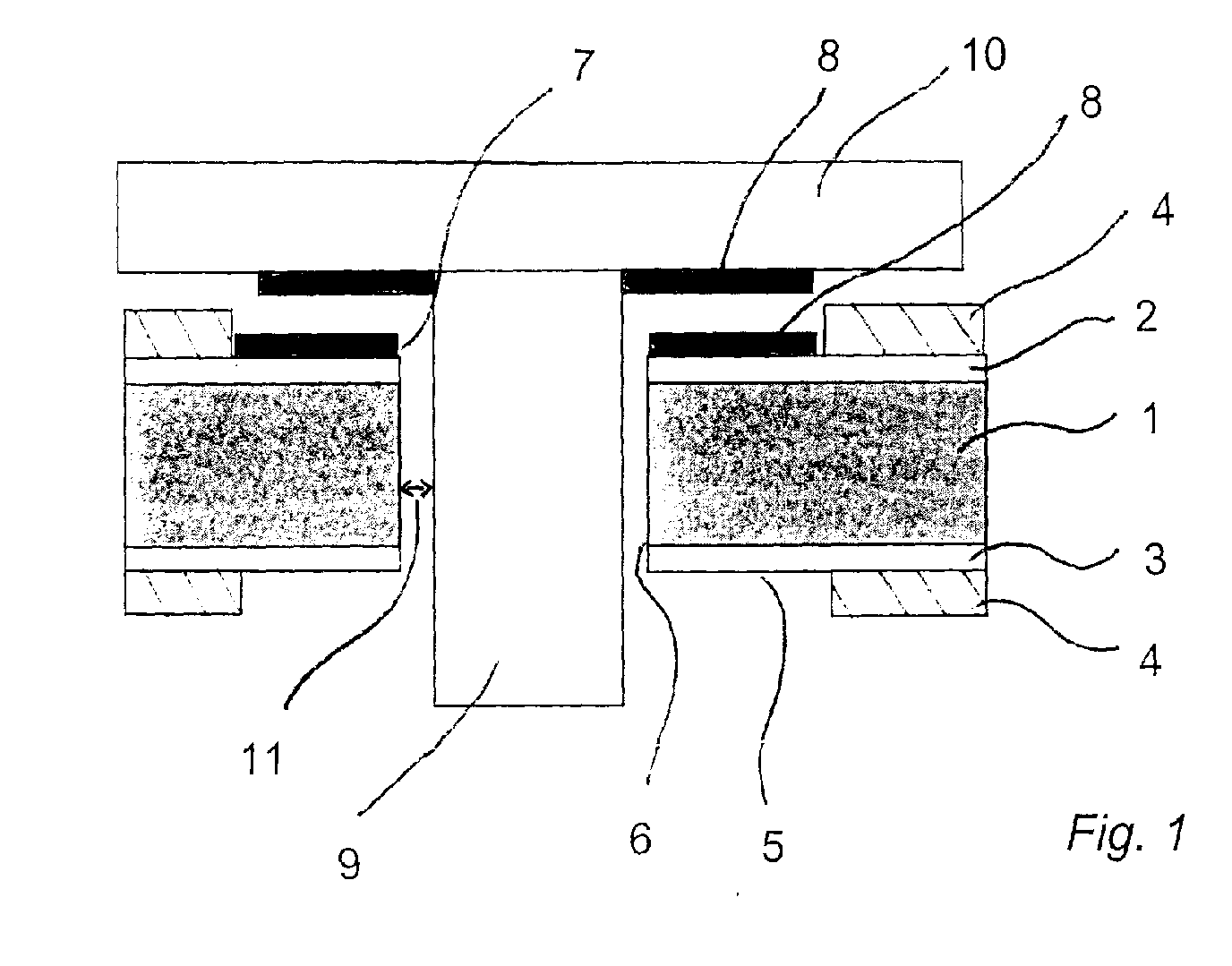
- 1 denotes a circuit board on the upper side of one first copper layer 2 and on the underside thereof a second copper layer 3 are upset.
- the first copper layer 2 is electrical insulating solder resist 4 partially covered.
- the same is the second Copper layer partially covered with the solder resist 4.
- a first one Contact point 5 is circular. It is marginalized by the Solder resist 4 limited.
- the first contact point 5 has a central one Breakthrough 6 on.
- On the top of the board 1 is one second contact point 7 formed, which is also circular through the solder resist 4 is limited.
- the second contact point 7 also has the central breakthrough 6 on.
- the second contact point 7 is additionally coated with a solder 8 here. Lot 8 can e.g. be applied by a printing process.
- connection element 9 With 9 a connection element of a component 10 is designated.
- the Connection element 9 passes through the opening 6. Its free end protrudes the level formed by the first contact point 5 on the underside of the Board 1. Between the connecting element 9 and the inside of the Breakthrough 6, an annular gap 11 is formed.
- the embodiment of Figure 1 is in the soldered state shown.
- the molten solder 12 flows by the action of capillary forces in the annular gap 11 and comes finally in contact with the fixed solder 8, which is on the second Contact point 7 is applied.
- the solder 8 melts as a result of contact with the molten solder 12.
- it can also be caused by direct contact with the connecting element 9 heated by the molten solder 12 melt, then penetrate from above into the annular gap 11 and deal with the unite ascending lot 12. It forms on the second Contact point 7 a Lotmeniskus, which in turn in contact with a Component 10 provided layer of solder 8 comes.
- FIG 3 a forming solder joint is shown, in which the additional application of a solder 8 on the second contact point 7 and the Component 10 has been dispensed with.
- too molten solder is drawn into the annular gap 11 by capillary forces and reaches the second contact point 7.
- the weight of the Component 10 through the formed solder connection directly to the second Contact point 7 removed.
- the method can then be carried out particularly effectively be when the diameter of the further openings 13 and the Gap distance of the annular gap 11 are chosen so that by means of capillary forces the molten solder 12 to the surface of the second contact point 7 is moved.
- To support the movement of the molten solder 12 it is also possible to close the top of the circuit board 1 with a vacuum act upon.
Landscapes
- Engineering & Computer Science (AREA)
- Manufacturing & Machinery (AREA)
- Microelectronics & Electronic Packaging (AREA)
- Electric Connection Of Electric Components To Printed Circuits (AREA)
- Coupling Device And Connection With Printed Circuit (AREA)
- Multi-Conductor Connections (AREA)
- Manufacturing Of Electrical Connectors (AREA)
Abstract
Description
- Vorsehen einer ersten Kontaktstelle auf der Unterseite der Platine und einer zweiten Kontaktstelle in gegenüberliegender Anordnung auf der Oberseite der Platine,
- Durchführen des Anschlusselements durch einen die erste und die zweite Kontaktstelle durchgreifenden Durchbruch, so dass das freie Ende des Anschlusselements über eine durch die erste Kontaktstelle beschriebene Ebene hervorsteht und zwischen der Wand des Durchbruchs und dem Anschlusselement ein Ringspalt gebildet ist und
- Aufbringen eines schmelzflüssigen Lots auf die erste Kontaktstelle und das freie Ende des Anschlusselements, so dass das Lot in den Ringspalt eindringt und entlang des Anschlusselements zur zweiten Kontaktstelle (7) fließt und eine Lötverbindung zwischen der ersten und der zweiten (7) Kontaktstelle und dem Anschlusselement (9) gebildet wird.
Diese Aufgabe wird durch die Merkmale der Ansprüche 1 und 8 gelöst. Zweckmäßige Ausgestaltungen ergeben sich aus den Merkmalen der Ansprüche 2 bis 7.
- Fig.1
- einen schematischen Querschnitt eines ersten Ausführungsbeispiels,
- Fig.2
- das Ausführungsbeispiel nach Fig.1 im verlöteten Zustand,
- Fig.3
- eine Querschnittsansicht eines zweiten Ausführungsbeispiels im verlöteten Zustand und
- Fig.4
- eine Querschnittsansicht eines dritten Ausführungsbeispiels im verlöteten Zustand.
- 1
- Platine
- 2
- erste Kupferschicht
- 3
- zweite Kupferschicht
- 4
- Lötstoplack
- 5
- erste Kontaktstelle
- 6
- Durchbruch
- 7
- zweite Kontaktstelle
- 8
- Lötschicht
- 9
- Anschlußelement
- 10
- Bauelement
- 11
- Ringspalt
- 12
- schmelzflüssiges Lot
- 13
- weiterer Durchbruch
Claims (9)
- Verfahren zur Herstellung einer Lötverbindung eines Anschlusselements (9) mit einer auf der Platine (1) vorgesehenen Kontaktstelle (5,7) mit folgenden Schritten:dadurch gekennzeichnet, dassVersehen einer ersten Kontaktstelle (5) auf der Unterseite der Platine (1) und einer zweiten Kontaktstelle (7) in gegenüberliegender Anordnung auf der Oberseite der Platine (1),Durchführung eines Anschlusselements (9) durch einen die erste (5) und die zweite Kontaktstelle (7) durchgreifenden Durchbruch (6), so dass das freie Ende des Anschlusselements (9) über eine durch die erste Kontaktstelle (5) beschriebene Ebene hervorsteht und zwischen der Wand des Durchbruches (6) und dem Anschlusselement (9) ein Ringspalt (11) gebildet ist undAufbringen eines schmelzflüssigen Lots (12) auf die erste Kontaktstelle (5) und das freie Ende des Anschlusselements (9), so dass das Lot (12) in den Ringspalt (11) eindringt und entlang des Anschlusselements (9) zur zweiten Kontaktstelle (7) fließt, und eine Lötverbindung zwischen der ersten (5) und der zweiten Kontaktstelle (7) und dem Anschlusselement (9) gebildet wird
ein mit dem Anschlusselement (9) verbundenes Bauelement (10) in der Nähe der zweiten Kontaktstelle (7) derart angeordnet wird, dass das Lot (12) das Bauelement (10) mit der zweiten Kontaktstelle (7) verbindet. - Verfahren nach Anspruch 1, wobei eine Spaltbreite des Ringspalts (11) so dimensioniert wird, daß das Lot (12) durch Kapillarkräfte von der ersten (5) zur zweiten Kontaktstelle (7) bewegt wird.
- Verfahren nach einem der vorhergehenden Ansprüche, wobei vor der Herstellung der Lötverbindung auf die erste (5) und/oder zweite Kontaktstelle (7) eine aus Lot (8) hergestellte Schicht aufgebracht wird.
- Verfahren nach einem der vorhergehenden Ansprüche, wobei mindestens ein weiterer die erste (5) mit der zweiten Kontaktstelle (7) verbindender Durchbruch (13) vorgesehen ist.
- Verfahren nach einem der vorhergehenden Ansprüche, wobei der Durchmesser des weiteren Durchbruchs (13) so dimensioniert ist, daß das Lot (12) durch Kapillarkräfte von der ersten (5) zur zweiten Kontaktstelle (7) bewegt wird.
- Verfahren nach einem der vorhergehenden Ansprüche, wobei der weitere Durchbruch (13) im Randbereich der Kontaktstellen (5, 7) vorgesehen ist.
- Verfahren nach einem der vorhergehenden Ansprüche, wobei ein mit dem Anschlußelement (9) verbundenes Bauelement (10) in der Nähe der zweiten Kontaktstelle (7) derart angeordnet wird, daß das Lot (12) das Bauelement (10) mit der zweiten Kontaktstelle (7) verbindet.
- Schaltung mit einer nach einem der Ansprüche 1 bis 7 hergestellten Lötverbindung.
- Schaltung mit einer nach einem der Ansprüche 1 - 8 hergestellten Lötverbindung.
Applications Claiming Priority (2)
| Application Number | Priority Date | Filing Date | Title |
|---|---|---|---|
| DE19963108 | 1999-12-24 | ||
| DE19963108A DE19963108C1 (de) | 1999-12-24 | 1999-12-24 | Verfahren zur Herstellung einer Lötverbindung und Schaltung mit einer solchen Lötverbindung |
Publications (3)
| Publication Number | Publication Date |
|---|---|
| EP1111974A2 true EP1111974A2 (de) | 2001-06-27 |
| EP1111974A3 EP1111974A3 (de) | 2003-05-14 |
| EP1111974B1 EP1111974B1 (de) | 2007-10-31 |
Family
ID=7934572
Family Applications (1)
| Application Number | Title | Priority Date | Filing Date |
|---|---|---|---|
| EP00127521A Expired - Lifetime EP1111974B1 (de) | 1999-12-24 | 2000-12-15 | Verfahren zur Herstellung einer Lötverbindung |
Country Status (3)
| Country | Link |
|---|---|
| EP (1) | EP1111974B1 (de) |
| AT (1) | ATE377344T1 (de) |
| DE (2) | DE19963108C1 (de) |
Families Citing this family (2)
| Publication number | Priority date | Publication date | Assignee | Title |
|---|---|---|---|---|
| DE10331840A1 (de) * | 2003-07-14 | 2005-02-24 | Rosenberger Hochfrequenztechnik Gmbh & Co. Kg | Bauteil für eine Leiterplatte und Verfahren zum Bestücken der Leiterplatte mit diesem Bauteil |
| CN114485597B (zh) * | 2022-02-10 | 2022-12-09 | 南通天正信息技术服务有限公司 | 一种投影对点测量铅垂器具及其加工装置 |
Family Cites Families (10)
| Publication number | Priority date | Publication date | Assignee | Title |
|---|---|---|---|---|
| CH375051A (de) * | 1959-10-14 | 1964-02-15 | Schweiz Wagons Aufzuegefab | Verfahren zur Herstellung elektrisch leitender Lötverbindungen bei gedruckten Schaltungen |
| US3500538A (en) * | 1966-08-29 | 1970-03-17 | Gen Electric | Method for producing a wire having improved soldering characteristics |
| DE2657313B2 (de) * | 1976-12-17 | 1978-10-12 | Siemens Ag, 1000 Berlin Und 8000 Muenchen | Verfahren zum Verbinden elektrischer Bauelemente mit den Leiterbahnen einer Leiter- oder Trägerplatte |
| US4477970A (en) * | 1982-04-01 | 1984-10-23 | Motorola, Inc. | P.C. Board mounting method for surface mounted components |
| DE3231056A1 (de) * | 1982-08-20 | 1984-02-23 | Siemens AG, 1000 Berlin und 8000 München | Verfahren zum aufbringen von unbedrahteten bauelementen auf leiterplatten |
| FI84413C (fi) * | 1988-10-27 | 1991-11-25 | Salora Oy | Genomfoering foer att dubbelsidigt kretskort samt foerfarande foer aostadkommande av densamma. |
| JPH057077A (ja) * | 1991-04-26 | 1993-01-14 | Matsushita Electric Works Ltd | 半田付け方法 |
| JPH06132656A (ja) * | 1992-10-19 | 1994-05-13 | Cmk Corp | プリント配線板における導通用部品 |
| JPH10335775A (ja) * | 1997-05-29 | 1998-12-18 | Fuji Electric Co Ltd | プリント回路板 |
| JPH11251733A (ja) * | 1998-02-27 | 1999-09-17 | Fuji Xerox Co Ltd | プリント基板へのリード部品実装方法 |
-
1999
- 1999-12-24 DE DE19963108A patent/DE19963108C1/de not_active Expired - Fee Related
-
2000
- 2000-12-15 DE DE50014742T patent/DE50014742D1/de not_active Expired - Fee Related
- 2000-12-15 EP EP00127521A patent/EP1111974B1/de not_active Expired - Lifetime
- 2000-12-15 AT AT00127521T patent/ATE377344T1/de not_active IP Right Cessation
Also Published As
| Publication number | Publication date |
|---|---|
| EP1111974B1 (de) | 2007-10-31 |
| EP1111974A3 (de) | 2003-05-14 |
| ATE377344T1 (de) | 2007-11-15 |
| DE50014742D1 (de) | 2007-12-13 |
| DE19963108C1 (de) | 2001-06-21 |
Similar Documents
| Publication | Publication Date | Title |
|---|---|---|
| EP0301533B1 (de) | Elektrische Sicherung und Verfahren zu ihrer Herstellung | |
| DE102006013506B4 (de) | Elektrischer Steckeranschluss | |
| EP2516321B1 (de) | Sensor mit einem vorzugsweise mehrschichtigen keramiksubstrat und verfahren zu dessen herstellung | |
| DE19809138A1 (de) | Leiterplatte mit SMD-Bauelementen | |
| EP3817881B1 (de) | Verfahren zur herstellung einer hochtemperaturfesten bleifreien lotverbindung und anordnung mit einer hochtemperaturfesten bleifreien lotverbindung | |
| EP0166105B1 (de) | Flexible Leiterplatte und Verfahren zu ihrer Herstellung | |
| DE69429293T2 (de) | Autoglasscheibe mit einer gedruckten Leiterstruktur | |
| EP1665914B1 (de) | Leiterplatte mit einer haltevorrichtung zum halten bedrahteter elektronischer bauteile, verfahren zur herstellung einer solchen leiterplatte und deren verwendung in einem lötofen | |
| EP2543240A1 (de) | Elektrische kontaktanordnung | |
| DE60128537T2 (de) | Zusammenbau zur verbindung von mindestens zwei gedruckten schaltungen | |
| EP1080615B1 (de) | Mehrfachnutzen für elektronische bauelemente, sowie verfahren zum aufbau von bumps, lotrahmen, abstandshalter und dergl. auf dem mehrfachnutzen | |
| WO2002093992A1 (de) | Leiterplatte mit einer darauf aufgebrachten kontakthülse | |
| EP0710432B1 (de) | Verfahren zur herstellung von folienleiterplatten oder halbzeugen für folienleiterplatten sowie nach dem verfahren hergestellte folienleiterplatten und halbzeuge | |
| DE10045534A1 (de) | Elektronisches Bauteil mit Außenanschlußelementen | |
| DE19963108C1 (de) | Verfahren zur Herstellung einer Lötverbindung und Schaltung mit einer solchen Lötverbindung | |
| AT12738U1 (de) | Verfahren und system zum bereitstellen eines insbesondere eine mehrzahl von leiterplattenelementen enthaltenden plattenförmigen gegenstands | |
| DE102008017152B4 (de) | Verfahren zum Herstellen einer elektrischen und/oder mechanischen Verbindung zwischen einer Leiterplatte und einem Kontaktpartner sowie Verbundsystem | |
| DE69605271T2 (de) | Verfahren zur Herstellung von flexiblen gedruckten Leiterplatten, insbesondere für Motorfahrzeuge, und dabei hergestellte gedruckte Leiterplatten | |
| DE10064221B4 (de) | Leiterplatine mit gekühltem SMD-Baustein | |
| DE102015102505B4 (de) | Leiterplatte | |
| DE2820002A1 (de) | Elektrisches anschlussbauteil fuer die bestueckung einer elektrischen leiterplatte | |
| EP0144413A1 (de) | Leiterplatte zum auflöten von integrierten miniaturschaltungen und verfahren zur herstellung von solchen leiterplatten | |
| EP0298410A1 (de) | Elektrisches Bauteil mit Anschlussstiften | |
| EP0905824A2 (de) | Elektrischer Verbinder | |
| DE102019129971A1 (de) | Verfahren zum Auflöten eines Bauelements auf eine Leiterplatte, Elektronikeinheit und Feldgerät der Automatisierungstechnik |
Legal Events
| Date | Code | Title | Description |
|---|---|---|---|
| PUAI | Public reference made under article 153(3) epc to a published international application that has entered the european phase |
Free format text: ORIGINAL CODE: 0009012 |
|
| AK | Designated contracting states |
Kind code of ref document: A2 Designated state(s): AT BE CH CY DE DK ES FI FR GB GR IE IT LI LU MC NL PT SE TR |
|
| AX | Request for extension of the european patent |
Free format text: AL;LT;LV;MK;RO;SI |
|
| PUAL | Search report despatched |
Free format text: ORIGINAL CODE: 0009013 |
|
| AK | Designated contracting states |
Designated state(s): AT BE CH CY DE DK ES FI FR GB GR IE IT LI LU MC NL PT SE TR |
|
| AX | Request for extension of the european patent |
Extension state: AL LT LV MK RO SI |
|
| 17P | Request for examination filed |
Effective date: 20031029 |
|
| AKX | Designation fees paid |
Designated state(s): AT BE CH CY DE DK ES FI FR GB GR IE IT LI LU MC NL PT SE TR |
|
| RAP1 | Party data changed (applicant data changed or rights of an application transferred) |
Owner name: GRUNDIG MULTIMEDIA B.V. |
|
| GRAP | Despatch of communication of intention to grant a patent |
Free format text: ORIGINAL CODE: EPIDOSNIGR1 |
|
| GRAS | Grant fee paid |
Free format text: ORIGINAL CODE: EPIDOSNIGR3 |
|
| GRAA | (expected) grant |
Free format text: ORIGINAL CODE: 0009210 |
|
| AK | Designated contracting states |
Kind code of ref document: B1 Designated state(s): AT BE CH CY DE DK ES FI FR GB GR IE IT LI LU MC NL PT SE TR |
|
| REG | Reference to a national code |
Ref country code: GB Ref legal event code: FG4D Free format text: NOT ENGLISH |
|
| REG | Reference to a national code |
Ref country code: IE Ref legal event code: FG4D Free format text: LANGUAGE OF EP DOCUMENT: GERMAN |
|
| REG | Reference to a national code |
Ref country code: CH Ref legal event code: EP |
|
| REF | Corresponds to: |
Ref document number: 50014742 Country of ref document: DE Date of ref document: 20071213 Kind code of ref document: P |
|
| NLV1 | Nl: lapsed or annulled due to failure to fulfill the requirements of art. 29p and 29m of the patents act | ||
| PG25 | Lapsed in a contracting state [announced via postgrant information from national office to epo] |
Ref country code: SE Free format text: LAPSE BECAUSE OF FAILURE TO SUBMIT A TRANSLATION OF THE DESCRIPTION OR TO PAY THE FEE WITHIN THE PRESCRIBED TIME-LIMIT Effective date: 20080131 Ref country code: NL Free format text: LAPSE BECAUSE OF FAILURE TO SUBMIT A TRANSLATION OF THE DESCRIPTION OR TO PAY THE FEE WITHIN THE PRESCRIBED TIME-LIMIT Effective date: 20071031 Ref country code: ES Free format text: LAPSE BECAUSE OF FAILURE TO SUBMIT A TRANSLATION OF THE DESCRIPTION OR TO PAY THE FEE WITHIN THE PRESCRIBED TIME-LIMIT Effective date: 20080211 |
|
| GBV | Gb: ep patent (uk) treated as always having been void in accordance with gb section 77(7)/1977 [no translation filed] | ||
| PG25 | Lapsed in a contracting state [announced via postgrant information from national office to epo] |
Ref country code: PT Free format text: LAPSE BECAUSE OF FAILURE TO SUBMIT A TRANSLATION OF THE DESCRIPTION OR TO PAY THE FEE WITHIN THE PRESCRIBED TIME-LIMIT Effective date: 20080331 |
|
| REG | Reference to a national code |
Ref country code: IE Ref legal event code: FD4D |
|
| BERE | Be: lapsed |
Owner name: GRUNDIG MULTIMEDIA B.V. Effective date: 20071231 |
|
| PG25 | Lapsed in a contracting state [announced via postgrant information from national office to epo] |
Ref country code: MC Free format text: LAPSE BECAUSE OF NON-PAYMENT OF DUE FEES Effective date: 20071231 Ref country code: DK Free format text: LAPSE BECAUSE OF FAILURE TO SUBMIT A TRANSLATION OF THE DESCRIPTION OR TO PAY THE FEE WITHIN THE PRESCRIBED TIME-LIMIT Effective date: 20071031 |
|
| REG | Reference to a national code |
Ref country code: CH Ref legal event code: PL |
|
| EN | Fr: translation not filed | ||
| PLBE | No opposition filed within time limit |
Free format text: ORIGINAL CODE: 0009261 |
|
| STAA | Information on the status of an ep patent application or granted ep patent |
Free format text: STATUS: NO OPPOSITION FILED WITHIN TIME LIMIT |
|
| PG25 | Lapsed in a contracting state [announced via postgrant information from national office to epo] |
Ref country code: BE Free format text: LAPSE BECAUSE OF NON-PAYMENT OF DUE FEES Effective date: 20071231 |
|
| 26N | No opposition filed |
Effective date: 20080801 |
|
| PG25 | Lapsed in a contracting state [announced via postgrant information from national office to epo] |
Ref country code: IE Free format text: LAPSE BECAUSE OF FAILURE TO SUBMIT A TRANSLATION OF THE DESCRIPTION OR TO PAY THE FEE WITHIN THE PRESCRIBED TIME-LIMIT Effective date: 20071031 Ref country code: LI Free format text: LAPSE BECAUSE OF NON-PAYMENT OF DUE FEES Effective date: 20071231 Ref country code: CH Free format text: LAPSE BECAUSE OF NON-PAYMENT OF DUE FEES Effective date: 20071231 Ref country code: FR Free format text: LAPSE BECAUSE OF FAILURE TO SUBMIT A TRANSLATION OF THE DESCRIPTION OR TO PAY THE FEE WITHIN THE PRESCRIBED TIME-LIMIT Effective date: 20080704 Ref country code: DE Free format text: LAPSE BECAUSE OF NON-PAYMENT OF DUE FEES Effective date: 20080701 |
|
| PG25 | Lapsed in a contracting state [announced via postgrant information from national office to epo] |
Ref country code: GB Free format text: LAPSE BECAUSE OF FAILURE TO SUBMIT A TRANSLATION OF THE DESCRIPTION OR TO PAY THE FEE WITHIN THE PRESCRIBED TIME-LIMIT Effective date: 20071031 |
|
| PG25 | Lapsed in a contracting state [announced via postgrant information from national office to epo] |
Ref country code: GR Free format text: LAPSE BECAUSE OF FAILURE TO SUBMIT A TRANSLATION OF THE DESCRIPTION OR TO PAY THE FEE WITHIN THE PRESCRIBED TIME-LIMIT Effective date: 20080201 |
|
| PG25 | Lapsed in a contracting state [announced via postgrant information from national office to epo] |
Ref country code: FI Free format text: LAPSE BECAUSE OF FAILURE TO SUBMIT A TRANSLATION OF THE DESCRIPTION OR TO PAY THE FEE WITHIN THE PRESCRIBED TIME-LIMIT Effective date: 20071031 |
|
| PG25 | Lapsed in a contracting state [announced via postgrant information from national office to epo] |
Ref country code: AT Free format text: LAPSE BECAUSE OF NON-PAYMENT OF DUE FEES Effective date: 20071215 |
|
| PG25 | Lapsed in a contracting state [announced via postgrant information from national office to epo] |
Ref country code: CY Free format text: LAPSE BECAUSE OF FAILURE TO SUBMIT A TRANSLATION OF THE DESCRIPTION OR TO PAY THE FEE WITHIN THE PRESCRIBED TIME-LIMIT Effective date: 20071031 |
|
| PG25 | Lapsed in a contracting state [announced via postgrant information from national office to epo] |
Ref country code: LU Free format text: LAPSE BECAUSE OF NON-PAYMENT OF DUE FEES Effective date: 20071215 |
|
| PG25 | Lapsed in a contracting state [announced via postgrant information from national office to epo] |
Ref country code: TR Free format text: LAPSE BECAUSE OF FAILURE TO SUBMIT A TRANSLATION OF THE DESCRIPTION OR TO PAY THE FEE WITHIN THE PRESCRIBED TIME-LIMIT Effective date: 20071031 |
|
| PG25 | Lapsed in a contracting state [announced via postgrant information from national office to epo] |
Ref country code: IT Free format text: LAPSE BECAUSE OF NON-PAYMENT OF DUE FEES Effective date: 20071231 |