EP1111974B1 - Procédé de fabrication d'une connexion à soudage - Google Patents
Procédé de fabrication d'une connexion à soudage Download PDFInfo
- Publication number
- EP1111974B1 EP1111974B1 EP00127521A EP00127521A EP1111974B1 EP 1111974 B1 EP1111974 B1 EP 1111974B1 EP 00127521 A EP00127521 A EP 00127521A EP 00127521 A EP00127521 A EP 00127521A EP 1111974 B1 EP1111974 B1 EP 1111974B1
- Authority
- EP
- European Patent Office
- Prior art keywords
- contact point
- solder
- terminal element
- annular gap
- circuit board
- Prior art date
- Legal status (The legal status is an assumption and is not a legal conclusion. Google has not performed a legal analysis and makes no representation as to the accuracy of the status listed.)
- Expired - Lifetime
Links
Images

Classifications
-
- H—ELECTRICITY
- H05—ELECTRIC TECHNIQUES NOT OTHERWISE PROVIDED FOR
- H05K—PRINTED CIRCUITS; CASINGS OR CONSTRUCTIONAL DETAILS OF ELECTRIC APPARATUS; MANUFACTURE OF ASSEMBLAGES OF ELECTRICAL COMPONENTS
- H05K3/00—Apparatus or processes for manufacturing printed circuits
- H05K3/30—Assembling printed circuits with electric components, e.g. with resistors
- H05K3/32—Assembling printed circuits with electric components, e.g. with resistors electrically connecting electric components or wires to printed circuits
- H05K3/34—Assembling printed circuits with electric components, e.g. with resistors electrically connecting electric components or wires to printed circuits by soldering
- H05K3/3447—Lead-in-hole components
-
- H—ELECTRICITY
- H05—ELECTRIC TECHNIQUES NOT OTHERWISE PROVIDED FOR
- H05K—PRINTED CIRCUITS; CASINGS OR CONSTRUCTIONAL DETAILS OF ELECTRIC APPARATUS; MANUFACTURE OF ASSEMBLAGES OF ELECTRICAL COMPONENTS
- H05K2201/00—Indexing scheme relating to printed circuits covered by H05K1/00
- H05K2201/09—Shape and layout
- H05K2201/09209—Shape and layout details of conductors
- H05K2201/09654—Shape and layout details of conductors covering at least two types of conductors provided for in H05K2201/09218 - H05K2201/095
- H05K2201/0979—Redundant conductors or connections, i.e. more than one current path between two points
-
- H—ELECTRICITY
- H05—ELECTRIC TECHNIQUES NOT OTHERWISE PROVIDED FOR
- H05K—PRINTED CIRCUITS; CASINGS OR CONSTRUCTIONAL DETAILS OF ELECTRIC APPARATUS; MANUFACTURE OF ASSEMBLAGES OF ELECTRICAL COMPONENTS
- H05K2201/00—Indexing scheme relating to printed circuits covered by H05K1/00
- H05K2201/10—Details of components or other objects attached to or integrated in a printed circuit board
- H05K2201/10227—Other objects, e.g. metallic pieces
- H05K2201/10295—Metallic connector elements partly mounted in a hole of the PCB
- H05K2201/10303—Pin-in-hole mounted pins
-
- H—ELECTRICITY
- H05—ELECTRIC TECHNIQUES NOT OTHERWISE PROVIDED FOR
- H05K—PRINTED CIRCUITS; CASINGS OR CONSTRUCTIONAL DETAILS OF ELECTRIC APPARATUS; MANUFACTURE OF ASSEMBLAGES OF ELECTRICAL COMPONENTS
- H05K2201/00—Indexing scheme relating to printed circuits covered by H05K1/00
- H05K2201/10—Details of components or other objects attached to or integrated in a printed circuit board
- H05K2201/10613—Details of electrical connections of non-printed components, e.g. special leads
- H05K2201/10742—Details of leads
- H05K2201/1075—Shape details
- H05K2201/10871—Leads having an integral insert stop
-
- H—ELECTRICITY
- H05—ELECTRIC TECHNIQUES NOT OTHERWISE PROVIDED FOR
- H05K—PRINTED CIRCUITS; CASINGS OR CONSTRUCTIONAL DETAILS OF ELECTRIC APPARATUS; MANUFACTURE OF ASSEMBLAGES OF ELECTRICAL COMPONENTS
- H05K3/00—Apparatus or processes for manufacturing printed circuits
- H05K3/30—Assembling printed circuits with electric components, e.g. with resistors
- H05K3/32—Assembling printed circuits with electric components, e.g. with resistors electrically connecting electric components or wires to printed circuits
- H05K3/34—Assembling printed circuits with electric components, e.g. with resistors electrically connecting electric components or wires to printed circuits by soldering
- H05K3/3465—Application of solder
- H05K3/3468—Application of molten solder, e.g. dip soldering
-
- H—ELECTRICITY
- H05—ELECTRIC TECHNIQUES NOT OTHERWISE PROVIDED FOR
- H05K—PRINTED CIRCUITS; CASINGS OR CONSTRUCTIONAL DETAILS OF ELECTRIC APPARATUS; MANUFACTURE OF ASSEMBLAGES OF ELECTRICAL COMPONENTS
- H05K3/00—Apparatus or processes for manufacturing printed circuits
- H05K3/40—Forming printed elements for providing electric connections to or between printed circuits
- H05K3/4038—Through-connections; Vertical interconnect access [VIA] connections
- H05K3/4046—Through-connections; Vertical interconnect access [VIA] connections using auxiliary conductive elements, e.g. metallic spheres, eyelets, pieces of wire
Definitions
- the invention relates to a method for producing a solder joint of a connection element with a contact point provided on a circuit board. It also relates to a circuit.
- a solder joint of connecting elements with contact points of a circuit board is usually produced by wave soldering.
- a bottom of the board with molten solder is applied.
- the molten solder adheres to the contact points and these contact points by cross-connecting elements.
- the connection elements are firmly connected after solidification of the solder electrically conductive with the first contact points. -
- the weight of the device is removed via the solder joint thus prepared on the board. Over time, caused by heating or vibration, due to voltage in the solder to changes in the crystal structure. This can lead to breakage of the solder joint.
- Such a broken solder joint is also referred to as a "cold solder joint".
- circuit boards which are provided on both sides with a copper layer.
- the copper layer is used to create electrical connection paths.
- the openings are here surrounded directly by the contact elements, but not encased in a conductive manner.
- the copper layer is usually not used for the production of electrical connection paths, but for shielding.
- the copper layer has recesses in the area of the openings. Otherwise, the copper layer provided on the upper side is covered with an electrically insulating solder resist.
- EP 0 367 076 A is a method for the through-connection of a double-sided printed circuit board known. In this case, components are carried out via openings in the printed circuit board and soldered on the underside.
- solder pads are produced at the locations on the component side of the printed circuit board, at which after the application of the bare components, their connections rest.
- solder surfaces are also generated.
- the holes connecting the pads are incorporated into the circuit board, these holes are then metallized, it being noted that the components do not completely cover the holes during application. Subsequently, the applied components are soldered in a machine soldering process.
- the object of the invention is to eliminate the disadvantages of the prior art.
- a method is to be specified with which a durable solder joint is produced in the simplest possible and cost-effective manner.
- This object is solved by the features of claims 1 and 8.
- Advantageous embodiments emerge from the features of claims 2 to 7.
- solder joint can be made using the conventional wave soldering method.
- the gap width of the annular gap is dimensioned so that the solder is moved by capillary forces from the first to the second contact point. It may be dispensed in this case on separate means for moving the solder from the first to the second contact point.
- separate means may be, for example, means for generating a vacuum acting on the annular gap.
- a layer made of solder to be applied to the first and / or second contact point before the soldering connection is produced.
- a layer melts particularly easily upon contact with the molten solder. It can be rolled or printed on the first and / or second contact point.
- At least one further the first connecting with the second contact point breakthrough may be provided.
- the diameter of the further breakthrough is expediently dimensioned so that the solder is moved by capillary forces from the first to the second contact point.
- the further breakthrough may be provided in the edge region of the contact points. In the case of the provision of several further breakthroughs, these are advantageously arranged in a coronary manner around the circumference of the contact points. The proposed embodiment contributes to a particularly fast and secure formation of the solder bridge connecting the first and second contact points.
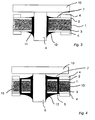
- 1 denotes a printed circuit board, on the upper side of which a first copper layer 2 is applied and on the underside of which a second copper layer 3 is applied.
- the first copper layer 2 is partially covered with an electrically insulating Lötstoplack 4.
- the second copper layer is partially covered with the Lötstoplack 4.
- a first contact point 5 is circular. It is bordered by the Lötstoplack 4.
- the first contact point 5 has a central opening 6.
- a second contact point 7 is formed on the upper side of the board 1, which is also limited in a circle by the Lötstoplack 4.
- the second contact point 7 has the central opening 6.
- the second contact point 7 is additionally coated here with a solder 8.
- the solder 8 may e.g. be applied by a printing process.
- connection element of a device 10 is designated.
- the connecting element 9 penetrates the opening 6. Its free end protrudes beyond the plane formed by the first contact point 5 on the underside of the board 1. Between the connection element 9 and the inside of the opening 6, an annular gap 11 is formed.
- FIG 2 the embodiment of Figure 1 is shown in the soldered state.
- the free end of the connecting element 9 is acted upon with molten solder 12.
- the molten solder 12 flows through the action of capillary forces in the annular gap 11 and finally comes into contact with the solid solder 8, which is applied to the second contact point 7.
- the solder 8 melts due to the contact with the molten solder 12. It can also melt by direct contact with the heated by the molten solder 12 connecting element 9, then penetrate from above into the annular gap 11 and unite with the rising therein solder 12.
- a solder meniscus forms on the second contact point 7, which in turn comes into contact with a layer of the solder 8 provided on the component 10. As a result, this layer is melted.
- solder joint is formed between the first contact point 5, the second contact point 7, the connection element 9 and the component 10.
- the dead weight of the component 10 is removed directly onto the second contact point 7.
- the solder joint thus produced is particularly durable. The risk of breakage of such a solder joint is minimal.
- FIG 3 a forming solder joint is shown in which has been dispensed with the additional application of a solder 8 on the second contact point 7 and the device 10. Also in this case, the molten solder is drawn by capillary forces into the annular gap 11 and reaches the second contact point 7. Again, the weight of the device 10 is removed by the formed solder joint directly to the second contact point 7.
- the method can be carried out particularly effectively, in particular, if the diameter of the further openings 13 and the gap spacing of the annular gap 11 are selected so that the molten solder 12 is moved to the surface of the second contact point 7 by means of capillary forces. In order to assist the movement of the molten solder 12, it is also possible to apply a negative pressure to the upper side of the board 1.
Landscapes
- Engineering & Computer Science (AREA)
- Manufacturing & Machinery (AREA)
- Microelectronics & Electronic Packaging (AREA)
- Electric Connection Of Electric Components To Printed Circuits (AREA)
- Coupling Device And Connection With Printed Circuit (AREA)
- Manufacturing Of Electrical Connectors (AREA)
- Multi-Conductor Connections (AREA)
Claims (7)
- Procédé pour réaliser une liaison brasée d'un élément de raccordement (9) avec un emplacement de contact (5, 7) prévu sur une platine (1), comprenant les étapes suivantes :- on prévoit un premier emplacement de contact (5) sur la face inférieure de la platine (1) et un second emplacement de contact (7) dans un agencement opposé sur la face supérieure de la platine (1),- on fait passer un élément de raccordement (9) à travers une traversée (6) qui passe à travers le premier (5) et le second emplacement de contact (7), de sorte que l'extrémité libre de l'élément de raccordement (9) dépasse au-delà d'un plan défini par le premier emplacement de contact (5) et qu'il se forme une fente annulaire (11) entre la paroi de la traversée (6) et l'élément de raccordement (9), et- on applique un produit de brasage (12) à l'état liquide fondu sur le premier emplacement de contact (5) et l'extrémité libre de l'élément de raccordement (9), de sorte que le produit de brasage (12) pénètre dans la fente annulaire (11) et s'écoule le long de l'élément de raccordement (9) vers le second emplacement de contact (7) et qu'il se forme une liaison brasée entre le premier (5) et le second emplacement de contact (7) et l'élément de raccordement (9),caractérisé en ce qu'on agence un composant (10) relié à l'élément de raccordement (9) au voisinage du second emplacement de contact (7) de telle sorte que le produit de brasage (12) relie le composant (10) au second emplacement de contact (7).
- Procédé selon la revendication 1, dans lequel la largeur de la fente annulaire (11) est dimensionnée de telle façon que le produit de brasage (12) est déplacé par des forces capillaires du premier (5) au second emplacement de contact (7).
- Procédé selon l'une des revendications précédentes, dans lequel avant la réalisation de la liaison brasée on applique sur le premier (5) et/ou sur le second emplacement de contact (7) une couche produite en produit de brasage (8).
- Procédé selon l'une des revendications précédentes, dans lequel il est prévu au moins une autre traversée (13) qui relie le premier (5) au second emplacement de contact (7).
- Procédé selon l'une des revendications précédentes, dans lequel le diamètre de l'autre traversée (13) est dimensionné de telle façon que le produit de brasage (12) est déplacé par des forces capillaires du premier (5) au second emplacement de contact (7).
- Procédé selon l'une des revendications précédentes, dans lequel l'autre traversée (13) est prévue dans la zone de bordure des emplacements de contact (5, 7).
- Circuit comprenant une liaison brasée réalisée selon les revendications 1 à 6, d'un élément de raccordement (9) avec un emplacement de contact (5, 7) prévu sur la platine (1), présentant les caractéristiques suivantes :- un premier emplacement de contact (5) sur la face inférieure de la platine (1) et un second emplacement de contact (7) dans un agencement opposé sur la face supérieure de la platine (1),- un élément de raccordement (9) qui est passé à travers une traversée (6) qui passe à travers le premier (5) et le second emplacement de contact (7), de sorte que l'extrémité libre de l'élément de raccordement (9) dépasse au-delà d'un plan défini par le premier emplacement de contact (5) et qu'il se forme une fente annulaire (11) entre la paroi de la traversée (6) et l'élément de raccordement (9), et dans lequel- la liaison brasée entre le premier (5) et le second emplacement de contact (7) et l'élément de raccordement (9) est formée par application d'un produit de brasage (12) à l'état liquide fondu sur le premier emplacement de contact (5) et l'extrémité libre de l'élément de raccordement (9), de sorte que le produit de brasage (12) pénètre dans la fente annulaire (11) et s'écoule le long de l'élément de raccordement (9) vers le second emplacement de contact (7),caractérisé en ce qu'un composant (10) relié à l'élément de raccordement (9) est agencé au voisinage du second emplacement de contact (7) de telle sorte que le produit de brasage (12) relie le composant (10) au second emplacement de contact (7).
Applications Claiming Priority (2)
| Application Number | Priority Date | Filing Date | Title |
|---|---|---|---|
| DE19963108A DE19963108C1 (de) | 1999-12-24 | 1999-12-24 | Verfahren zur Herstellung einer Lötverbindung und Schaltung mit einer solchen Lötverbindung |
| DE19963108 | 1999-12-24 |
Publications (3)
| Publication Number | Publication Date |
|---|---|
| EP1111974A2 EP1111974A2 (fr) | 2001-06-27 |
| EP1111974A3 EP1111974A3 (fr) | 2003-05-14 |
| EP1111974B1 true EP1111974B1 (fr) | 2007-10-31 |
Family
ID=7934572
Family Applications (1)
| Application Number | Title | Priority Date | Filing Date |
|---|---|---|---|
| EP00127521A Expired - Lifetime EP1111974B1 (fr) | 1999-12-24 | 2000-12-15 | Procédé de fabrication d'une connexion à soudage |
Country Status (3)
| Country | Link |
|---|---|
| EP (1) | EP1111974B1 (fr) |
| AT (1) | ATE377344T1 (fr) |
| DE (2) | DE19963108C1 (fr) |
Families Citing this family (2)
| Publication number | Priority date | Publication date | Assignee | Title |
|---|---|---|---|---|
| DE10331840A1 (de) * | 2003-07-14 | 2005-02-24 | Rosenberger Hochfrequenztechnik Gmbh & Co. Kg | Bauteil für eine Leiterplatte und Verfahren zum Bestücken der Leiterplatte mit diesem Bauteil |
| CN114485597B (zh) * | 2022-02-10 | 2022-12-09 | 南通天正信息技术服务有限公司 | 一种投影对点测量铅垂器具及其加工装置 |
Family Cites Families (10)
| Publication number | Priority date | Publication date | Assignee | Title |
|---|---|---|---|---|
| CH375051A (de) * | 1959-10-14 | 1964-02-15 | Schweiz Wagons Aufzuegefab | Verfahren zur Herstellung elektrisch leitender Lötverbindungen bei gedruckten Schaltungen |
| US3500538A (en) * | 1966-08-29 | 1970-03-17 | Gen Electric | Method for producing a wire having improved soldering characteristics |
| DE2657313B2 (de) * | 1976-12-17 | 1978-10-12 | Siemens Ag, 1000 Berlin Und 8000 Muenchen | Verfahren zum Verbinden elektrischer Bauelemente mit den Leiterbahnen einer Leiter- oder Trägerplatte |
| US4477970A (en) * | 1982-04-01 | 1984-10-23 | Motorola, Inc. | P.C. Board mounting method for surface mounted components |
| DE3231056A1 (de) * | 1982-08-20 | 1984-02-23 | Siemens AG, 1000 Berlin und 8000 München | Verfahren zum aufbringen von unbedrahteten bauelementen auf leiterplatten |
| FI84413C (fi) * | 1988-10-27 | 1991-11-25 | Salora Oy | Genomfoering foer att dubbelsidigt kretskort samt foerfarande foer aostadkommande av densamma. |
| JPH057077A (ja) * | 1991-04-26 | 1993-01-14 | Matsushita Electric Works Ltd | 半田付け方法 |
| JPH06132656A (ja) * | 1992-10-19 | 1994-05-13 | Cmk Corp | プリント配線板における導通用部品 |
| JPH10335775A (ja) * | 1997-05-29 | 1998-12-18 | Fuji Electric Co Ltd | プリント回路板 |
| JPH11251733A (ja) * | 1998-02-27 | 1999-09-17 | Fuji Xerox Co Ltd | プリント基板へのリード部品実装方法 |
-
1999
- 1999-12-24 DE DE19963108A patent/DE19963108C1/de not_active Expired - Fee Related
-
2000
- 2000-12-15 AT AT00127521T patent/ATE377344T1/de not_active IP Right Cessation
- 2000-12-15 EP EP00127521A patent/EP1111974B1/fr not_active Expired - Lifetime
- 2000-12-15 DE DE50014742T patent/DE50014742D1/de not_active Expired - Fee Related
Also Published As
| Publication number | Publication date |
|---|---|
| DE19963108C1 (de) | 2001-06-21 |
| EP1111974A2 (fr) | 2001-06-27 |
| ATE377344T1 (de) | 2007-11-15 |
| EP1111974A3 (fr) | 2003-05-14 |
| DE50014742D1 (de) | 2007-12-13 |
Similar Documents
| Publication | Publication Date | Title |
|---|---|---|
| DE2852753C3 (de) | Verfahren zum Befestigen von Bauelementen mit flächigen Anschlußkontakten auf einer Leiterplatte und Schablone zur Durchführung des Verfahrens | |
| DE102006013506B4 (de) | Elektrischer Steckeranschluss | |
| EP0166105B1 (fr) | Plaquette flexible et son procédé de fabrication | |
| EP1665914B1 (fr) | Carte de circuits imprimes comprenant un dispositif de maintien concu pour maintenir des composants electroniques cables, procede pour produire une telle carte de circuits imprimes et son utilisation dans un four a braser | |
| DE4446509A1 (de) | Verfahren zur Herstellung von Leiterbahnen auf einem Vertiefungen aufweisenden Substrat | |
| EP3817881A1 (fr) | Procédé de fabrication d'un joint brasé sans plomb résistant aux températures élevées, et joint brasé sans plomb résistant aux températures élevées | |
| EP2543240A1 (fr) | Système de contact électrique | |
| EP0867932B1 (fr) | Procédé pour la fabrication de connexions à fil | |
| EP1393604A1 (fr) | Carte de circuits imprimes sur laquelle un connecteur femelle est monte | |
| EP0613331B1 (fr) | Méthode d'attachement d'un circuit hybride sur un circuit imprimé | |
| DE10045534B4 (de) | Elektronisches Bauteil mit Außenanschlußelementen ausgebildet als Kapillarelement, Verfahren zur Herstellung und Anordnung | |
| EP0710432B1 (fr) | Procede de fabrication de circuits imprimes en feuilles ou de produits semi-finis destines a la fabrication de circuits imprimes en feuilles, ainsi que circuits imprimes en feuilles et produits semi-finis fabriques selon ce procede | |
| DE19963108C1 (de) | Verfahren zur Herstellung einer Lötverbindung und Schaltung mit einer solchen Lötverbindung | |
| DE10064221B4 (de) | Leiterplatine mit gekühltem SMD-Baustein | |
| DE2820002A1 (de) | Elektrisches anschlussbauteil fuer die bestueckung einer elektrischen leiterplatte | |
| EP0298410A1 (fr) | Composant électrique aux broches de connexion | |
| EP0144413A1 (fr) | Carte imprimee pour le montage en surface de circuits integres miniature et procede de fabrication de telles cartes imprimees | |
| DE4208594A1 (de) | Verfahren zur herstellung einer elektrischen, vorgefertigten baueinheit und deren befestigung auf einer leiterplatte | |
| EP0751562A2 (fr) | Fixation thermiquement conductive d'un dispositif électronique de puissance sur une plaquette de circuit avec dissipateur de chaleur | |
| DE3925155C2 (fr) | ||
| EP0905824A2 (fr) | Connecteur électrique | |
| DE4008658C2 (fr) | ||
| DE102019129971A1 (de) | Verfahren zum Auflöten eines Bauelements auf eine Leiterplatte, Elektronikeinheit und Feldgerät der Automatisierungstechnik | |
| DE19814428B4 (de) | Leiterplatte mit großflächigen, mit Lotdepots versehenen Kontaktierungsflächen (Lotpads) | |
| DE10334634B3 (de) | Verfahren zum seitlichen Kontaktieren eines Halbleiterchips |
Legal Events
| Date | Code | Title | Description |
|---|---|---|---|
| PUAI | Public reference made under article 153(3) epc to a published international application that has entered the european phase |
Free format text: ORIGINAL CODE: 0009012 |
|
| AK | Designated contracting states |
Kind code of ref document: A2 Designated state(s): AT BE CH CY DE DK ES FI FR GB GR IE IT LI LU MC NL PT SE TR |
|
| AX | Request for extension of the european patent |
Free format text: AL;LT;LV;MK;RO;SI |
|
| PUAL | Search report despatched |
Free format text: ORIGINAL CODE: 0009013 |
|
| AK | Designated contracting states |
Designated state(s): AT BE CH CY DE DK ES FI FR GB GR IE IT LI LU MC NL PT SE TR |
|
| AX | Request for extension of the european patent |
Extension state: AL LT LV MK RO SI |
|
| 17P | Request for examination filed |
Effective date: 20031029 |
|
| AKX | Designation fees paid |
Designated state(s): AT BE CH CY DE DK ES FI FR GB GR IE IT LI LU MC NL PT SE TR |
|
| RAP1 | Party data changed (applicant data changed or rights of an application transferred) |
Owner name: GRUNDIG MULTIMEDIA B.V. |
|
| GRAP | Despatch of communication of intention to grant a patent |
Free format text: ORIGINAL CODE: EPIDOSNIGR1 |
|
| GRAS | Grant fee paid |
Free format text: ORIGINAL CODE: EPIDOSNIGR3 |
|
| GRAA | (expected) grant |
Free format text: ORIGINAL CODE: 0009210 |
|
| AK | Designated contracting states |
Kind code of ref document: B1 Designated state(s): AT BE CH CY DE DK ES FI FR GB GR IE IT LI LU MC NL PT SE TR |
|
| REG | Reference to a national code |
Ref country code: GB Ref legal event code: FG4D Free format text: NOT ENGLISH |
|
| REG | Reference to a national code |
Ref country code: IE Ref legal event code: FG4D Free format text: LANGUAGE OF EP DOCUMENT: GERMAN |
|
| REG | Reference to a national code |
Ref country code: CH Ref legal event code: EP |
|
| REF | Corresponds to: |
Ref document number: 50014742 Country of ref document: DE Date of ref document: 20071213 Kind code of ref document: P |
|
| NLV1 | Nl: lapsed or annulled due to failure to fulfill the requirements of art. 29p and 29m of the patents act | ||
| PG25 | Lapsed in a contracting state [announced via postgrant information from national office to epo] |
Ref country code: SE Free format text: LAPSE BECAUSE OF FAILURE TO SUBMIT A TRANSLATION OF THE DESCRIPTION OR TO PAY THE FEE WITHIN THE PRESCRIBED TIME-LIMIT Effective date: 20080131 Ref country code: NL Free format text: LAPSE BECAUSE OF FAILURE TO SUBMIT A TRANSLATION OF THE DESCRIPTION OR TO PAY THE FEE WITHIN THE PRESCRIBED TIME-LIMIT Effective date: 20071031 Ref country code: ES Free format text: LAPSE BECAUSE OF FAILURE TO SUBMIT A TRANSLATION OF THE DESCRIPTION OR TO PAY THE FEE WITHIN THE PRESCRIBED TIME-LIMIT Effective date: 20080211 |
|
| GBV | Gb: ep patent (uk) treated as always having been void in accordance with gb section 77(7)/1977 [no translation filed] | ||
| PG25 | Lapsed in a contracting state [announced via postgrant information from national office to epo] |
Ref country code: PT Free format text: LAPSE BECAUSE OF FAILURE TO SUBMIT A TRANSLATION OF THE DESCRIPTION OR TO PAY THE FEE WITHIN THE PRESCRIBED TIME-LIMIT Effective date: 20080331 |
|
| REG | Reference to a national code |
Ref country code: IE Ref legal event code: FD4D |
|
| BERE | Be: lapsed |
Owner name: GRUNDIG MULTIMEDIA B.V. Effective date: 20071231 |
|
| PG25 | Lapsed in a contracting state [announced via postgrant information from national office to epo] |
Ref country code: MC Free format text: LAPSE BECAUSE OF NON-PAYMENT OF DUE FEES Effective date: 20071231 Ref country code: DK Free format text: LAPSE BECAUSE OF FAILURE TO SUBMIT A TRANSLATION OF THE DESCRIPTION OR TO PAY THE FEE WITHIN THE PRESCRIBED TIME-LIMIT Effective date: 20071031 |
|
| REG | Reference to a national code |
Ref country code: CH Ref legal event code: PL |
|
| EN | Fr: translation not filed | ||
| PLBE | No opposition filed within time limit |
Free format text: ORIGINAL CODE: 0009261 |
|
| STAA | Information on the status of an ep patent application or granted ep patent |
Free format text: STATUS: NO OPPOSITION FILED WITHIN TIME LIMIT |
|
| PG25 | Lapsed in a contracting state [announced via postgrant information from national office to epo] |
Ref country code: BE Free format text: LAPSE BECAUSE OF NON-PAYMENT OF DUE FEES Effective date: 20071231 |
|
| 26N | No opposition filed |
Effective date: 20080801 |
|
| PG25 | Lapsed in a contracting state [announced via postgrant information from national office to epo] |
Ref country code: IE Free format text: LAPSE BECAUSE OF FAILURE TO SUBMIT A TRANSLATION OF THE DESCRIPTION OR TO PAY THE FEE WITHIN THE PRESCRIBED TIME-LIMIT Effective date: 20071031 Ref country code: LI Free format text: LAPSE BECAUSE OF NON-PAYMENT OF DUE FEES Effective date: 20071231 Ref country code: CH Free format text: LAPSE BECAUSE OF NON-PAYMENT OF DUE FEES Effective date: 20071231 Ref country code: FR Free format text: LAPSE BECAUSE OF FAILURE TO SUBMIT A TRANSLATION OF THE DESCRIPTION OR TO PAY THE FEE WITHIN THE PRESCRIBED TIME-LIMIT Effective date: 20080704 Ref country code: DE Free format text: LAPSE BECAUSE OF NON-PAYMENT OF DUE FEES Effective date: 20080701 |
|
| PG25 | Lapsed in a contracting state [announced via postgrant information from national office to epo] |
Ref country code: GB Free format text: LAPSE BECAUSE OF FAILURE TO SUBMIT A TRANSLATION OF THE DESCRIPTION OR TO PAY THE FEE WITHIN THE PRESCRIBED TIME-LIMIT Effective date: 20071031 |
|
| PG25 | Lapsed in a contracting state [announced via postgrant information from national office to epo] |
Ref country code: GR Free format text: LAPSE BECAUSE OF FAILURE TO SUBMIT A TRANSLATION OF THE DESCRIPTION OR TO PAY THE FEE WITHIN THE PRESCRIBED TIME-LIMIT Effective date: 20080201 |
|
| PG25 | Lapsed in a contracting state [announced via postgrant information from national office to epo] |
Ref country code: FI Free format text: LAPSE BECAUSE OF FAILURE TO SUBMIT A TRANSLATION OF THE DESCRIPTION OR TO PAY THE FEE WITHIN THE PRESCRIBED TIME-LIMIT Effective date: 20071031 |
|
| PG25 | Lapsed in a contracting state [announced via postgrant information from national office to epo] |
Ref country code: AT Free format text: LAPSE BECAUSE OF NON-PAYMENT OF DUE FEES Effective date: 20071215 |
|
| PG25 | Lapsed in a contracting state [announced via postgrant information from national office to epo] |
Ref country code: CY Free format text: LAPSE BECAUSE OF FAILURE TO SUBMIT A TRANSLATION OF THE DESCRIPTION OR TO PAY THE FEE WITHIN THE PRESCRIBED TIME-LIMIT Effective date: 20071031 |
|
| PG25 | Lapsed in a contracting state [announced via postgrant information from national office to epo] |
Ref country code: LU Free format text: LAPSE BECAUSE OF NON-PAYMENT OF DUE FEES Effective date: 20071215 |
|
| PG25 | Lapsed in a contracting state [announced via postgrant information from national office to epo] |
Ref country code: TR Free format text: LAPSE BECAUSE OF FAILURE TO SUBMIT A TRANSLATION OF THE DESCRIPTION OR TO PAY THE FEE WITHIN THE PRESCRIBED TIME-LIMIT Effective date: 20071031 |
|
| PG25 | Lapsed in a contracting state [announced via postgrant information from national office to epo] |
Ref country code: IT Free format text: LAPSE BECAUSE OF NON-PAYMENT OF DUE FEES Effective date: 20071231 |