EP1112607B1 - Ensemble platine-contact enfichable - Google Patents
Ensemble platine-contact enfichable Download PDFInfo
- Publication number
- EP1112607B1 EP1112607B1 EP99953696A EP99953696A EP1112607B1 EP 1112607 B1 EP1112607 B1 EP 1112607B1 EP 99953696 A EP99953696 A EP 99953696A EP 99953696 A EP99953696 A EP 99953696A EP 1112607 B1 EP1112607 B1 EP 1112607B1
- Authority
- EP
- European Patent Office
- Prior art keywords
- board
- contact
- plug
- arrangement according
- housing
- Prior art date
- Legal status (The legal status is an assumption and is not a legal conclusion. Google has not performed a legal analysis and makes no representation as to the accuracy of the status listed.)
- Expired - Lifetime
Links
Images

Classifications
-
- H—ELECTRICITY
- H01—ELECTRIC ELEMENTS
- H01R—ELECTRICALLY-CONDUCTIVE CONNECTIONS; STRUCTURAL ASSOCIATIONS OF A PLURALITY OF MUTUALLY-INSULATED ELECTRICAL CONNECTING ELEMENTS; COUPLING DEVICES; CURRENT COLLECTORS
- H01R12/00—Structural associations of a plurality of mutually-insulated electrical connecting elements, specially adapted for printed circuits, e.g. printed circuit boards [PCB], flat or ribbon cables, or like generally planar structures, e.g. terminal strips, terminal blocks; Coupling devices specially adapted for printed circuits, flat or ribbon cables, or like generally planar structures; Terminals specially adapted for contact with, or insertion into, printed circuits, flat or ribbon cables, or like generally planar structures
- H01R12/70—Coupling devices
- H01R12/71—Coupling devices for rigid printing circuits or like structures
- H01R12/72—Coupling devices for rigid printing circuits or like structures coupling with the edge of the rigid printed circuits or like structures
- H01R12/721—Coupling devices for rigid printing circuits or like structures coupling with the edge of the rigid printed circuits or like structures cooperating directly with the edge of the rigid printed circuits
-
- H—ELECTRICITY
- H01—ELECTRIC ELEMENTS
- H01R—ELECTRICALLY-CONDUCTIVE CONNECTIONS; STRUCTURAL ASSOCIATIONS OF A PLURALITY OF MUTUALLY-INSULATED ELECTRICAL CONNECTING ELEMENTS; COUPLING DEVICES; CURRENT COLLECTORS
- H01R12/00—Structural associations of a plurality of mutually-insulated electrical connecting elements, specially adapted for printed circuits, e.g. printed circuit boards [PCB], flat or ribbon cables, or like generally planar structures, e.g. terminal strips, terminal blocks; Coupling devices specially adapted for printed circuits, flat or ribbon cables, or like generally planar structures; Terminals specially adapted for contact with, or insertion into, printed circuits, flat or ribbon cables, or like generally planar structures
- H01R12/50—Fixed connections
- H01R12/51—Fixed connections for rigid printed circuits or like structures
- H01R12/55—Fixed connections for rigid printed circuits or like structures characterised by the terminals
- H01R12/58—Fixed connections for rigid printed circuits or like structures characterised by the terminals terminals for insertion into holes
-
- H—ELECTRICITY
- H05—ELECTRIC TECHNIQUES NOT OTHERWISE PROVIDED FOR
- H05K—PRINTED CIRCUITS; CASINGS OR CONSTRUCTIONAL DETAILS OF ELECTRIC APPARATUS; MANUFACTURE OF ASSEMBLAGES OF ELECTRICAL COMPONENTS
- H05K1/00—Printed circuits
- H05K1/02—Details
- H05K1/0213—Electrical arrangements not otherwise provided for
- H05K1/0215—Grounding of printed circuits by connection to external grounding means
-
- H—ELECTRICITY
- H05—ELECTRIC TECHNIQUES NOT OTHERWISE PROVIDED FOR
- H05K—PRINTED CIRCUITS; CASINGS OR CONSTRUCTIONAL DETAILS OF ELECTRIC APPARATUS; MANUFACTURE OF ASSEMBLAGES OF ELECTRICAL COMPONENTS
- H05K3/00—Apparatus or processes for manufacturing printed circuits
- H05K3/30—Assembling printed circuits with electric components, e.g. with resistors
- H05K3/32—Assembling printed circuits with electric components, e.g. with resistors electrically connecting electric components or wires to printed circuits
- H05K3/325—Assembling printed circuits with electric components, e.g. with resistors electrically connecting electric components or wires to printed circuits by abutting or pinching; Mechanical auxiliary parts therefor
-
- H—ELECTRICITY
- H05—ELECTRIC TECHNIQUES NOT OTHERWISE PROVIDED FOR
- H05K—PRINTED CIRCUITS; CASINGS OR CONSTRUCTIONAL DETAILS OF ELECTRIC APPARATUS; MANUFACTURE OF ASSEMBLAGES OF ELECTRICAL COMPONENTS
- H05K2201/00—Indexing scheme relating to printed circuits covered by H05K1/00
- H05K2201/03—Conductive materials
- H05K2201/0302—Properties and characteristics in general
- H05K2201/0311—Metallic part with specific elastic properties, e.g. bent piece of metal as electrical contact
Definitions
- the invention relates to a circuit board plug contact arrangement with a plug contact unit having at least one contact pin and with one with the plug contact unit in electrical contactable circuit board.
- US-A-3,594,699 shows a circuit board plug contact arrangement, where the functions of the mechanical bracket and the electrical contacting of various components be perceived. So are on the plug contact arrangement projections made of insulating material are provided, which in a Snap the corresponding recess into the board.
- the electrical contacting is made by curved contact springs made on corresponding on the outside of the board Lay conductor tracks on. The mechanical connection between the board and the plug contact with regard to insertion and separation not specifically designed.
- US-A-3,858,957 shows a circuit board plug contact arrangement, in which the contact springs bulges to mechanical Have bracket. As with the contact arrangement shown there an easy connection and disconnection are not to be achieved intended for permanent locking of the contact partner.
- the at least one Contact pin a locking projection protruding transversely to the contact pin axis and the circuit board has at least one recess, in each of which a snap-in projection under production an electrical contact with the circuit board engages, wherein
- the snap-in projection each in a pointed Sliding flank and locking flank at an angle to the contact pin axis has, the acute angle between the slide-on flank and the contact pin axis is smaller than the tip Is the angle between the locking flank and the contact pin axis, a mechanical locking with the board and at the same time to ensure that the board can be easily pushed open.
- the contact plug is no longer on the board be attached. Because of the parallel as well as very close Arranging the contact pins on the board will provide good filtering the input and output signals and thus a low one Coupling effect of the contact pins with each other and to the inner one Area of the circuit board.
- the snap-in projection shows that it is easy to carry out one at an acute angle to the contact pin axis lying push-on flank and snap-in flank, the point Angle between the sliding flank and the contact pin axis smaller than the acute angle between the locking flank and the Contact pin axis is.
- a space-saving contact pin arrangement in the invention PCB plug contact arrangement is created by at least two board holes arranged in series on the Formed circuit board and arranged accordingly in accordance with contact pins are that the locking projections alternately the top and bottom of the board in the corresponding board arrangement engage. Such an arrangement is also straight cheap in such systems that are exposed to vibrations are. If several contact pins for one board alternately snap from the top and bottom of the board due to the elasticity of the thin contact pins Vibration-absorbing, elastic mounting of the board.
- Another advantageous embodiment for an inventive PCB plug contact arrangement is created by the board having several recesses in series and several corresponding contact pins in one plane, preferably is perpendicular to the board, arranged in such a way are that the length of the latching flank is based on one Side of the board increases towards the center of the board.
- a housing In order to seal the board watertight, a housing is included an insertion opening for the board on the plug contact unit arranged, the circuit board in the housing along a guide attached to the housing is inserted.
- the plug contact unit form integrally with the housing, preferably the plug contact unit and the housing made of plastic are poured.
- the at least one contact pin embedded in the plug contact unit is so that one of its two free ends into one of the housing surrounding inner connector area and that other free end of the contact pin in an outer connector area protrude.
- the board pushed into the housing is on the inside Plug area due to the locking of the snap-in projection of the at least one contact pin with the respective one Board recess can be defined at least in the sliding direction.
- circuit board plug contact arrangement with a housing can have larger components that take up a lot of space on the board claim to be arranged on the housing.
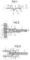
- a contact pin 1 can be seen, which has a locking projection 2 in the form of an asymmetrical nose.
- the latching projection 2 comprises a slide-on flank 3 and one Locking flank 4. Both flanks 3, 4 have an acute angle to the contact pin axis A.
- the acute angle w1 between the sliding flank 3 and the contact pin axis A is smaller than the acute angle w2 between the locking flank 4 and the Contact pin.
- An end piece closes on the sliding flank 3 5, which lies in the contact pin axis A.
- FIG. 2 two contact pins 1 are parallel to each other Contact pin axes A shown in a one contact pin holder 9 comprehensive plug contact unit 6 embedded are, the contact pin holder 9 made of an insulating Material is formed.
- the locking projections 2 of the contact pins 1 are arranged axially offset, with each latching flank 4 and insertion flank 3 from their contact pin axis A are directed away to the other contact pin 1.
- a circuit board 7 is inserted into the two contact pins 1 in the circuit board area that of the plug contact unit 6 is closest, has holes 8.
- the board 7 parallel to the fixed Contact pins 1 moved in the insertion direction E that the contact pins 1 due to the interaction between Slip-on flanks 3 of the contact pins 1 and the edge region 7 ' the board 7 and the sliding movement of the board 7 from this is bent away and thus elastically biased.
- the maximum preload is reached or maintained, when the nose of the locking projection 2 rests on the circuit board 7 or moved to the corresponding hole 8 becomes.
- the moment the asymmetrical nose of the Snap projection 2 of the contact pin 1 with the bore 8 of the Board 7 is aligned and snapped into it is the electrical one Contact between the contact pin and the not shown Printed circuit network of the board 7.
- the locking projection 2 of the lower contact pins 1 first clicks into the outer bore 8, this leaves again and then finally into the inner bore 8 locks.
- Fig. 3 there are four contact pins with the corresponding ones Bores 8 of the circuit board 7 snap-in projections 2 shown.
- the four contact pins 1 are in a common Plane that is perpendicular to that of the board 7 and the plane of the paper equivalent. To influence each other To avoid contact pins, they are sufficient Distance from each other, the length of the locking flank 4 of the contact pins 1 lying in one plane in relation to each one side of the board increases towards the middle of the board.
- FIG. 4 is a housing 10 of the circuit board plug contact arrangement according to the invention demonstrated.
- This housing includes one Insert opening 11 and a housing base 12, which in Fig. 4 has plug connector unit, not shown.
- the Circuit board 7 with electronic components arranged on it 15 is inserted into the housing 10 in the insertion direction E, the recesses, preferably designed as bores 8 13 arranged in the board at its edge region 14 are in the inserted state near the bottom of the case 12 is located.
- a convenient insertion as well as a accurate snapping of the locking projections 2 of the contact pins 1 in the recesses 13 is on the sides of the housing 16 arranged guide grooves 17 ensured.
- the contact pins 1 are in the contact pin holder 9 embedded and connected to this is a one-piece housing 10 arranged, the inner 18 and outer connector area 19 separates from each other. In the inner connector area 18 the contact pins 1 protrude with their snap-in projections 2, only two contact pins being shown in FIG together with the guide grooves 17, not shown, the position the board 7 set.
- the insertion opening 11 is optionally by means of a cover 20 closed with the help of sealing devices, in particular glued or welded.
- the outer plug area 19 the free ends of the Contact pins 1 without snap-in projection 2, the outer plug area 19 formed as the free end of a wire harness can be. In other words, in this case it follows free end of the wiring harness to the housing 10.
- the inside of the case emerging from the free end of the wiring harness Contact counterparts are designed as contact pins according to the invention, which is the inclusion of the inserted into the housing Boards 7 realized.
- the housing 10 shown in Figures 4 and 5 can also be dimensioned so that several boards 7 in the housing 10 inserted and from corresponding contact pins 1 under Making an electrical contact can be locked.
Landscapes
- Engineering & Computer Science (AREA)
- Microelectronics & Electronic Packaging (AREA)
- Metallurgy (AREA)
- Manufacturing & Machinery (AREA)
- Coupling Device And Connection With Printed Circuit (AREA)
- Multi-Conductor Connections (AREA)
- Connector Housings Or Holding Contact Members (AREA)
Claims (14)
- Ensemble circuit imprimé-contact embrochable comprenantdans lequel l'au moins une broche de contact (1) présente une saillie d'enclenchement (2) qui fait saillie transversalement à l'axe (A) de la broche de contact et le circuit imprimé (7) présente au moins un évidement (13) dans lequel une saillie d'enclenchement (2) s'engage en établissant un contact électrique avec le circuit imprimé (7),une unité de contact embrochable (6) présentant au moins une broche de contact élastique (1) etun circuit imprimé (7) qui peut être mis en contact électrique avec l'unité de contact embrochable (6),
caractérisé en ce que la saillie d'enclenchement (2) présente un flanc d'emmanchement (3) et un flanc d'enclenchement (4) qui forment chacun un angle aigu (w1, w2) avec l'axe de la broche de contact, l'angle aigu (w2) entre le flanc d'emmanchement (3) et l'axe (A) de la broche de contact étant plus petit que l'angle aigu (w2) entre le flanc d'enclenchement (4) et l'axe de la broche de contact, afin de garantir un blocage mécanique avec le circuit imprimé (7) et, en même temps, la simplicité de l'emmanchement du circuit imprimé (7). - Ensemble circuit imprimé-contact embrochable selon la revendication 1,
caractérisé en ce que l'au moins une broche de contact (1) présente un embout (5) qui fait suite au flanc d'emmanchement (3) et qui se trouve dans l'axe (A) de la broche de contact. - Ensemble circuit imprimé-contact embrochable selon une des revendications 1 ou 2,
caractérisé en ce que l'au moins une broche de contact (1) est réalisée, dans la région de la saillie d'enclenchement (2) en formant une arête vive vers l'évidement (13) ménagé dans le circuit imprimé (7). - Ensemble circuit imprimé-contact embrochable selon l'une des revendications 1 ou 3,
caractérisé en ce que l'au moins un évidement (13) ménagé dans le circuit imprimé (7) est constitué par un perçage (8). - Ensemble circuit imprimé-contact embrochable selon la revendication 4,
caractérisé en ce que la surface intérieure du perçage (8) est munie d'un revêtement métallique. - Ensemble circuit imprimé-contact embrochable selon l'une des revendications 4 ou 5, caractérisé en ce qu'au moins deux perçages (8) disposés en une rangée sont formés dans le circuit imprimé (7) et des broches de contact (1) sont disposées de façon correspondante de manière que les saillies d'enclenchement (2) s'enclenchent respectivement en alternance sur la face supérieure du circuit imprimé et sur la face inférieure du circuit imprimé, dans le perçage (8) correspondant.
- Ensemble circuit imprimé-contact embrochable selon l'une des revendications 1 à 6, caractérisé en ce que le circuit imprimé (7) présente plusieurs évidements (13) en une rangée et, de façon correspondante, plusieurs broches de contact (1) sont disposées dans un plan qui se trouve de préférence perpendiculairement au circuit imprimé (7), de telle manière que la longueur du flanc d'enclenchement (4) mesurée par rapport à une face du circuit imprimé (7), croisse en direction du centre du circuit imprimé.
- Ensemble circuit imprimé-contact embrochable selon l'une des revendications 1 à 7, caractérisé en ce que les différentes broches de contact (1) d'une unité de contact embrochable (6) sont en contact avec différents circuits imprimés.
- Ensemble circuit imprimé-contact embrochable selon l'une des revendications 1 à 8, caractérisé en ce qu'un boítier (10) est disposé sur l'unité de contact embrochable (6), le circuit imprimé (7) pouvant être emmanché dans le boítier (10) le long d'un guide (17) solidaire du boítier.
- Ensemble circuit imprimé-contact embrochable selon l'une des revendications 1 à 9, caractérisé en ce que l'unité de contact embrochable (6) est réalisée en une seule pièce avec le boítier (10), lequel présente une ouverture d'emmanchement (11) pour le circuit imprimé (7), l'unité de contact embrochable (6) et le boítier (10) étant de préférence moulés en matière plastique.
- Ensemble circuit imprimé-contact embrochable selon l'une des revendications 1 ou 10, caractérisé en ce que l'au moins une broche de contact (1) est disposée, de préférence noyée, dans l'unité de contact embrochable (6) de telle manière que l'une des ses extrémités libres fasse saillie dans une zone intérieure (18) du contacteur qui est entourée par le boítier (10) et l'autre dans une région extérieure (19) du contacteur, le circuit imprimé (7) emmanché dans le boítier (10) pouvant être bloqué sur la zone intérieure (18) du connecteur grâce à l'enclenchement de la saillie d'enclenchement (2) de l'au moins une broche de contact dans la direction de l'emmanchement (E).
- Ensemble circuit imprimé-contact embrochable selon l'une des revendications 10 ou 11, caractérisé en ce que l'ouverture d'emmanchement (11) du boítier (10) est obturée à joint étanche à l'eau par un couvercle (20).
- Ensemble circuit imprimé-contact embrochable selon l'une des revendications 11 ou 12, caractérisé en ce que la zone extérieure (19) du connecteur est disposée à l'extrémité d'un faisceau de câbles.
- Ensemble circuit imprimé-contact embrochable selon l'une des revendications 9 à 13, caractérisé en ce que plusieurs circuits imprimés (7) peuvent être emmanchés dans le boítier (10) au moyen de guides correspondants (17) et peuvent être enclenchés avec établissement d'un contact électrique avec les broches de contact (1) correspondantes.
Applications Claiming Priority (3)
| Application Number | Priority Date | Filing Date | Title |
|---|---|---|---|
| DE19841467A DE19841467A1 (de) | 1998-09-10 | 1998-09-10 | Platinen-Steckkontakt-Anordnung |
| DE19841467 | 1998-09-10 | ||
| PCT/DE1999/002783 WO2000016447A1 (fr) | 1998-09-10 | 1999-09-02 | Ensemble platine-contact enfichable |
Publications (2)
| Publication Number | Publication Date |
|---|---|
| EP1112607A1 EP1112607A1 (fr) | 2001-07-04 |
| EP1112607B1 true EP1112607B1 (fr) | 2002-06-12 |
Family
ID=7880547
Family Applications (1)
| Application Number | Title | Priority Date | Filing Date |
|---|---|---|---|
| EP99953696A Expired - Lifetime EP1112607B1 (fr) | 1998-09-10 | 1999-09-02 | Ensemble platine-contact enfichable |
Country Status (5)
| Country | Link |
|---|---|
| EP (1) | EP1112607B1 (fr) |
| JP (1) | JP2002525807A (fr) |
| KR (1) | KR20010075036A (fr) |
| DE (2) | DE19841467A1 (fr) |
| WO (1) | WO2000016447A1 (fr) |
Families Citing this family (2)
| Publication number | Priority date | Publication date | Assignee | Title |
|---|---|---|---|---|
| JP5969405B2 (ja) * | 2013-01-30 | 2016-08-17 | 日立オートモティブシステムズ株式会社 | 車載用電子モジュール |
| TW201519533A (zh) * | 2014-05-29 | 2015-05-16 | Kuang Ying Comp Equipment Co | 正反插電連接器之結構 |
Family Cites Families (5)
| Publication number | Priority date | Publication date | Assignee | Title |
|---|---|---|---|---|
| US3693052A (en) * | 1971-04-15 | 1972-09-19 | Warwick Electronics Inc | Electrical component mounting |
| DE3138285A1 (de) * | 1981-09-25 | 1983-04-07 | Siemens AG, 1000 Berlin und 8000 München | Mittels mehrerer reihen von leitenden stiften senkrecht auf eine leiterplatte steckbare traegerplatte und verfahren zur herstellung der traegerplatte |
| JPH05159829A (ja) * | 1991-12-09 | 1993-06-25 | Du Pont Singapore Pte Ltd | 電気ソケット |
| DE19609425A1 (de) * | 1996-03-11 | 1997-09-18 | Telefunken Microelectron | Einpreßstift |
| DE19706281A1 (de) * | 1997-02-18 | 1998-08-20 | Siemens Ag | Verfahren zur Herstellung einer Ausnehmung in einer Leiterplatte eines Kommunikationsendgerätes |
-
1998
- 1998-09-10 DE DE19841467A patent/DE19841467A1/de not_active Withdrawn
-
1999
- 1999-09-02 WO PCT/DE1999/002783 patent/WO2000016447A1/fr not_active Ceased
- 1999-09-02 DE DE59901759T patent/DE59901759D1/de not_active Expired - Fee Related
- 1999-09-02 KR KR1020017003123A patent/KR20010075036A/ko not_active Withdrawn
- 1999-09-02 EP EP99953696A patent/EP1112607B1/fr not_active Expired - Lifetime
- 1999-09-02 JP JP2000570875A patent/JP2002525807A/ja not_active Withdrawn
Also Published As
| Publication number | Publication date |
|---|---|
| EP1112607A1 (fr) | 2001-07-04 |
| KR20010075036A (ko) | 2001-08-09 |
| WO2000016447A1 (fr) | 2000-03-23 |
| DE59901759D1 (de) | 2002-07-18 |
| JP2002525807A (ja) | 2002-08-13 |
| DE19841467A1 (de) | 2000-04-13 |
Similar Documents
| Publication | Publication Date | Title |
|---|---|---|
| EP1814202B1 (fr) | Dispositif d'accouplement | |
| DE19813458B4 (de) | Elektrischer Verbinder | |
| EP0848459A2 (fr) | Connecteur de ligne pour circuit imprimé | |
| WO2014161965A1 (fr) | Dispositif de connexion | |
| EP2979333B1 (fr) | Connecteur à compensation de diaphonie | |
| DE102012102567B4 (de) | Verschiebbare Isolationsbarriere | |
| EP1953871A2 (fr) | Agencement d'un premier support de circuit sur un deuxième support de circuit | |
| DE10261536A1 (de) | Anschluß- und Verbindungsklemme für elektrische Leiter | |
| DE102016107898B4 (de) | Laterale Leiterplattenverbindung | |
| EP1112607B1 (fr) | Ensemble platine-contact enfichable | |
| DE19916949B4 (de) | Gehäuse, insbesondere Schloßgehäuse für einen Kraftfahrzeugtürverschluß, Getriebegehäuse oder dergleichen Leitungsträger | |
| DE4321067C1 (de) | Elektrische Anschlußklemme für wenigstens eine Leiterplatte | |
| EP0955702A1 (fr) | Dispositif de connexion pour plaque de circuit imprimé | |
| DE10338122B3 (de) | Schaltgeräte-Leiterplatten-Kombination | |
| DE10047126B4 (de) | Befestigungseinrichtung | |
| DE102017011113B4 (de) | Elektrisches Verbindungselement mit einer Stromschiene | |
| WO2001018913A1 (fr) | Dispositif de connexion par enfichage de lignes electriques | |
| DE102004031949B4 (de) | Elektrischer Steckverbinder | |
| DE102016220346B4 (de) | Steckverbindung von Leiterzügen wenigstens zweier beabstandet zueinander angeordneter Leiterplatten mit wenigstens einem Steckverbinder | |
| WO2005006501A1 (fr) | Coupleur hf destine a connecter une fiche coaxiale a une ligne de transmission hf sur une plaquette | |
| EP2833487B1 (fr) | Jeu de contacts pour une douille de raccordement | |
| DE202018107302U1 (de) | LED-Leiterplattenmodul und Leuchtensystem | |
| DE10342047A1 (de) | Elektrisches Verbindungselement | |
| EP1418645A1 (fr) | Organe de contact et assemblage de cartes de circuits imprimés | |
| WO2002073746A1 (fr) | Connecteur de lignes |
Legal Events
| Date | Code | Title | Description |
|---|---|---|---|
| PUAI | Public reference made under article 153(3) epc to a published international application that has entered the european phase |
Free format text: ORIGINAL CODE: 0009012 |
|
| 17P | Request for examination filed |
Effective date: 20010104 |
|
| AK | Designated contracting states |
Kind code of ref document: A1 Designated state(s): AT BE CH CY DE DK ES FI FR GB GR IE IT LI LU MC NL PT SE |
|
| GRAG | Despatch of communication of intention to grant |
Free format text: ORIGINAL CODE: EPIDOS AGRA |
|
| GRAG | Despatch of communication of intention to grant |
Free format text: ORIGINAL CODE: EPIDOS AGRA |
|
| GRAH | Despatch of communication of intention to grant a patent |
Free format text: ORIGINAL CODE: EPIDOS IGRA |
|
| 17Q | First examination report despatched |
Effective date: 20011130 |
|
| GRAH | Despatch of communication of intention to grant a patent |
Free format text: ORIGINAL CODE: EPIDOS IGRA |
|
| GRAA | (expected) grant |
Free format text: ORIGINAL CODE: 0009210 |
|
| AK | Designated contracting states |
Kind code of ref document: B1 Designated state(s): DE FR GB IT |
|
| REG | Reference to a national code |
Ref country code: GB Ref legal event code: FG4D Free format text: NOT ENGLISH |
|
| REF | Corresponds to: |
Ref document number: 59901759 Country of ref document: DE Date of ref document: 20020718 |
|
| REG | Reference to a national code |
Ref country code: IE Ref legal event code: FG4D Free format text: GERMAN |
|
| PGFP | Annual fee paid to national office [announced via postgrant information from national office to epo] |
Ref country code: FR Payment date: 20020930 Year of fee payment: 4 |
|
| ET | Fr: translation filed | ||
| REG | Reference to a national code |
Ref country code: IE Ref legal event code: FD4D Ref document number: 1112607E Country of ref document: IE |
|
| PG25 | Lapsed in a contracting state [announced via postgrant information from national office to epo] |
Ref country code: DE Free format text: LAPSE BECAUSE OF NON-PAYMENT OF DUE FEES Effective date: 20030401 |
|
| PLBE | No opposition filed within time limit |
Free format text: ORIGINAL CODE: 0009261 |
|
| STAA | Information on the status of an ep patent application or granted ep patent |
Free format text: STATUS: NO OPPOSITION FILED WITHIN TIME LIMIT |
|
| 26N | No opposition filed |
Effective date: 20030313 |
|
| PG25 | Lapsed in a contracting state [announced via postgrant information from national office to epo] |
Ref country code: GB Free format text: LAPSE BECAUSE OF NON-PAYMENT OF DUE FEES Effective date: 20030902 |
|
| GBPC | Gb: european patent ceased through non-payment of renewal fee | ||
| PG25 | Lapsed in a contracting state [announced via postgrant information from national office to epo] |
Ref country code: FR Free format text: LAPSE BECAUSE OF NON-PAYMENT OF DUE FEES Effective date: 20040528 |
|
| REG | Reference to a national code |
Ref country code: FR Ref legal event code: ST |
|
| PG25 | Lapsed in a contracting state [announced via postgrant information from national office to epo] |
Ref country code: IT Free format text: LAPSE BECAUSE OF NON-PAYMENT OF DUE FEES;WARNING: LAPSES OF ITALIAN PATENTS WITH EFFECTIVE DATE BEFORE 2007 MAY HAVE OCCURRED AT ANY TIME BEFORE 2007. THE CORRECT EFFECTIVE DATE MAY BE DIFFERENT FROM THE ONE RECORDED. Effective date: 20050902 |