EP1118101B1 - Entladungslampe für dielektrisch behinderte entladungen mit verbesserter elektrodenkonfiguration - Google Patents
Entladungslampe für dielektrisch behinderte entladungen mit verbesserter elektrodenkonfiguration Download PDFInfo
- Publication number
- EP1118101B1 EP1118101B1 EP99969838A EP99969838A EP1118101B1 EP 1118101 B1 EP1118101 B1 EP 1118101B1 EP 99969838 A EP99969838 A EP 99969838A EP 99969838 A EP99969838 A EP 99969838A EP 1118101 B1 EP1118101 B1 EP 1118101B1
- Authority
- EP
- European Patent Office
- Prior art keywords
- discharge lamp
- discharge
- cathode
- anode
- lamp according
- Prior art date
- Legal status (The legal status is an assumption and is not a legal conclusion. Google has not performed a legal analysis and makes no representation as to the accuracy of the status listed.)
- Expired - Lifetime
Links
- 238000004804 winding Methods 0.000 claims description 17
- 239000003990 capacitor Substances 0.000 claims description 9
- 238000003860 storage Methods 0.000 claims description 9
- 230000000694 effects Effects 0.000 claims description 6
- 230000008878 coupling Effects 0.000 claims description 4
- 238000010168 coupling process Methods 0.000 claims description 4
- 238000005859 coupling reaction Methods 0.000 claims description 4
- 230000004907 flux Effects 0.000 claims description 3
- 230000002787 reinforcement Effects 0.000 claims description 3
- 230000010355 oscillation Effects 0.000 claims description 2
- 239000000463 material Substances 0.000 claims 4
- 238000011017 operating method Methods 0.000 description 10
- 230000008901 benefit Effects 0.000 description 7
- 230000002349 favourable effect Effects 0.000 description 4
- OAICVXFJPJFONN-UHFFFAOYSA-N Phosphorus Chemical compound [P] OAICVXFJPJFONN-UHFFFAOYSA-N 0.000 description 3
- 239000011248 coating agent Substances 0.000 description 3
- 238000000576 coating method Methods 0.000 description 3
- 238000010586 diagram Methods 0.000 description 3
- 206010016754 Flashback Diseases 0.000 description 2
- 230000004888 barrier function Effects 0.000 description 2
- 230000009286 beneficial effect Effects 0.000 description 2
- 238000013461 design Methods 0.000 description 2
- 238000009826 distribution Methods 0.000 description 2
- 230000000737 periodic effect Effects 0.000 description 2
- 230000002123 temporal effect Effects 0.000 description 2
- 229910018072 Al 2 O 3 Inorganic materials 0.000 description 1
- 238000012935 Averaging Methods 0.000 description 1
- 229910010413 TiO 2 Inorganic materials 0.000 description 1
- 230000035508 accumulation Effects 0.000 description 1
- 238000009825 accumulation Methods 0.000 description 1
- 230000003321 amplification Effects 0.000 description 1
- 230000008859 change Effects 0.000 description 1
- 239000002800 charge carrier Substances 0.000 description 1
- 238000010276 construction Methods 0.000 description 1
- 230000001419 dependent effect Effects 0.000 description 1
- 238000011161 development Methods 0.000 description 1
- 230000005611 electricity Effects 0.000 description 1
- 238000011156 evaluation Methods 0.000 description 1
- 230000006355 external stress Effects 0.000 description 1
- 239000011521 glass Substances 0.000 description 1
- 238000005286 illumination Methods 0.000 description 1
- 238000002347 injection Methods 0.000 description 1
- 239000007924 injection Substances 0.000 description 1
- 238000010849 ion bombardment Methods 0.000 description 1
- 238000004519 manufacturing process Methods 0.000 description 1
- 238000000034 method Methods 0.000 description 1
- 230000005012 migration Effects 0.000 description 1
- 238000013508 migration Methods 0.000 description 1
- 238000012986 modification Methods 0.000 description 1
- 230000004048 modification Effects 0.000 description 1
- 238000003199 nucleic acid amplification method Methods 0.000 description 1
- 238000005457 optimization Methods 0.000 description 1
- 230000003071 parasitic effect Effects 0.000 description 1
- 230000002093 peripheral effect Effects 0.000 description 1
- 230000008092 positive effect Effects 0.000 description 1
- 238000007493 shaping process Methods 0.000 description 1
- 229910000679 solder Inorganic materials 0.000 description 1
- 238000012549 training Methods 0.000 description 1
- 229910052724 xenon Inorganic materials 0.000 description 1
- FHNFHKCVQCLJFQ-UHFFFAOYSA-N xenon atom Chemical compound [Xe] FHNFHKCVQCLJFQ-UHFFFAOYSA-N 0.000 description 1
Images




Classifications
-
- H—ELECTRICITY
- H01—ELECTRIC ELEMENTS
- H01J—ELECTRIC DISCHARGE TUBES OR DISCHARGE LAMPS
- H01J61/00—Gas-discharge or vapour-discharge lamps
- H01J61/02—Details
- H01J61/04—Electrodes; Screens; Shields
- H01J61/06—Main electrodes
- H01J61/067—Main electrodes for low-pressure discharge lamps
-
- H—ELECTRICITY
- H01—ELECTRIC ELEMENTS
- H01J—ELECTRIC DISCHARGE TUBES OR DISCHARGE LAMPS
- H01J61/00—Gas-discharge or vapour-discharge lamps
- H01J61/02—Details
- H01J61/04—Electrodes; Screens; Shields
- H01J61/06—Main electrodes
- H01J61/067—Main electrodes for low-pressure discharge lamps
- H01J61/0672—Main electrodes for low-pressure discharge lamps characterised by the construction of the electrode
Definitions
- This invention relates to a dielectrically impeded discharge designed discharge lamps.
- a discharge lamp has in a discharge vessel filled with a discharge medium, at least a cathode and at least one anode, wherein at least the anode is separated from the discharge medium by a dielectric layer.
- the operation of dielectrically impeded discharges in such Discharge lamps are not interested in detail here. Therefore, it will be up here referred to the prior art, in particular those still below cited documents.
- this invention is concerned with the electrode configuration in FIG a discharge lamp for dielectrically impeded discharges.
- the invention is based on known strip-shaped electrodes.
- strip-shaped electrodes are in particular discharge lamps provided in the form of flat radiators, consisting essentially of two plane-parallel and optionally connected by a frame plates consist.
- the strip-shaped electrodes are generally on formed one or more of the walls of these plates, wherein in a corresponding flat discharge volume between the plates dielectrically Disabled discharges can be generated.
- run the strip-shaped cathodes and anodes thereby substantially parallel to each other.
- strip electrodes are also used on other discharge lamps possible, in particular with different discharge vessel geometries. They can also be used on non-flat discharge vessels on interior or exterior surfaces deposited by the discharge vessel forming boundary walls be or independent of a discharge vessel wall, about a plate carrying the electrode strips inside the discharge vessel.
- the invention is therefore directed to strip-shaped electrodes, that on a wall of the discharge vessel or on a wall in the Discharge vessel are applied.
- the invention is thus based on a discharge lamp with a with a Discharge medium filled discharge vessel, a strip-shaped Cathode and a strip-shaped anode and a dielectric Layer between the anode and the discharge medium.
- Disabled discharges are in addition to a beneficial electrical behavior the electrode configuration as an electrical component further also the geometric properties of the electrode configuration or the with it to be generated discharge structures. It can be on the one hand the uniformity of light production both temporally and locally Respect, d. H. on the temporal fluctuation and on a very homogeneous surface distribution. Of course, there can be certain Inhomogeneous area distributions are intended to be. Further, for certain applications, for example in the field of flat panel backlighting or in the case of signal lamps beyond that also with the discharge lamp Areal luminance of interest to achieve.
- the present invention is based on the technical problem a discharge lamp for dielectrically impeded discharges with a improved electrode configuration as well as such a discharge lamp and further comprising a matching ballast lighting system specify.
- a discharge lamp the above-mentioned type, which is characterized in that the anode meandering, so that the distance between the cathode and the Anode is modulated by the meandering shape or
- the cathode and the anode meander run, wherein the meandering forms are locally out of phase with each other, so that the distance between the cathode and the anode through both Meandering is modulated.
- the invention relates to a lighting system with a of these two discharge lamps and a ballast that is pulsed to one Active power coupling is designed in the discharge lamp.
- the invention is with regard to the discharge lamp to consider in two variants.
- the first variant uses the invention meandering course of the electrodes only in the Anode ahead.
- the exact course of the strip-shaped cathode is Basically open, but should by the meandering shape of the anode of the Discharge relevant distance between the cathode and the anode modulated be.
- the cathode can be a straight strip shape or a have any other strip shape, as long as the modulation of the discharge distance not canceled by the meandering form or by influencing the discharge distance in such a way in a different way Form is superimposed that intended by the invention Effect is missed.
- a prerequisite for this first variant of the invention discussed here is that the anode of the discharge lamp with respect to the cathode in any Form excellent, so in principle distinguishable from the cathode is.
- This can, in principle, be the case in many different forms Simplest case in that between the cathode and the discharge medium no dielectric layer is located.
- the concerns Meander shape both types of electrodes, d. H. at least one cathode and at least one anode run meandering. It is envisaged that the meandering forms with respect to the modulation of the discharge distance reinforce each other between the cathode and the anode. To they run in opposite phases to each other.
- the invention is to be understood in general as far as the Meander shapes of the electrodes need not be periodic. Therefore, concerns the concept of antiphase may only be local and other Place altered periodicity and possibly also non-periodic Cases where, however, locally are essentially "mountain on valley” and “valley on the mountain ", so the electrodes in essentially the same places towards each other or away from each other.
- the meandering forms do not necessarily involve an algebraic addition of the the meander shape respectively associated "stroke" in the discharge distance direction must mean. Rather, the meandering forms in different Layers are also not necessarily parallel to each other have to go. For example, the electrode strips on opposite Be formed inside walls of a discharge vessel.
- the discharge distance between Cathode and anode by at least one meandering shape of an electrode is modulated.
- the respective locations of the locally smallest discharge gap form at the same time places the highest local field and thus preferred Starting points for individual discharge structures.
- the discharge lamps according to the invention are namely particularly advantageous in connection with a pulsed active power injection method, which is not described here. It is referred to on the WO 94/23 442 and DE-P 43 11 197.1.
- Operating method for dielectric barrier discharge lamps preferably arise largely spatially stable single discharge structures, in accordance with the coupled active power in different Number first in the places with the largest field strengths form between the electrodes. It can also be less localized Forming "curtain-like" discharge structures, in the context of this Invention are equivalent.
- the present invention is directed however, in the case referred to above as the first variant was based on a local field reinforcement by a shaping on sides the anode.
- the cited prior art Protrusions on the cathode.
- the state of the art was at that time namely, the idea that in the pulsed operating method occurring discharge structures at the cathode a rather pointed and have a rather fanned out shape at the anode. Accordingly should by geometric design of the cathode the corresponding Tip of the discharge structure are localized, therefore logically in essential punctiform lugs at the cathode are preferably considered were.
- a meandering anode - in combination with a meandering one Cathode according to the so-called second variant or not - provides significant advantages. So is a meandering shape over the already described nose-like According to the prior art capacitively much cheaper, because between the electrode strips to a significant proportion of the electrode length can be significantly longer distances than the actual for the discharges significant distance at the places where the Electrodes come closest. With a reduced capacity of the electrode configuration and thus lower reactive currents can be, however the ballasts necessary for the operation of the discharge lamps design smaller and thus save costs, construction volume and weight. Further can with smaller capacities to be operated steeper pulse edges and thus better overall pulse shapes are realized.
- the discharge lamp sees a Electrode configuration of a plurality of cathodes and a plurality Anodes ago, which are arranged alternately in individual strips. This means, in each case only one anode strip between two cathode strips runs and vice versa.
- this embodiment meet the capacitive points of view, with respect to the opposite of electrodes Polarity surrounded electrodes even to a greater extent. Incidentally, this embodiment with its advantages applies to both initially distinguished variants of the invention.
- the strip-shaped cathode has no such meandering shape.
- she can in particular in the context of this first variant in conventional Way straight.
- z. B. at particularly large discharge intervals have straight cathode strips have the advantage that they are in the direction transverse to the strip direction a dense arrangement of the individual strips Enable discharge structures. It can by an inventively meandering anode form again on the mutual interference of the Individual discharge structures are taken into account.
- the meandering forms of two of them Cathode of adjacent anodes locally in phase with each other to an alternating arrangement of the discharge preferential sites on both sides to achieve the cathode.
- the first criterion relates to the relationship between the fluctuation of the discharge distance, ie the difference between the maximum discharge distance d max within half a period length and the minimum discharge distance d min in the same half period, and this half period length of the meander shape, hereinafter referred to with the abbreviation SL
- a value of 0.6 has been found to be favorable.
- the second criterion concerns the minimum already referred to Discharge distance in its relationship to the maximum occurring discharge gap in terms of actually in interpretive mode the discharge lamp occurring discharge structures.
- Discharge distance in its relationship to the maximum occurring discharge gap in terms of actually in interpretive mode the discharge lamp occurring discharge structures.
- a single discharge structure is present in both in the case of relatively localized discharge structures as well as in the already mentioned “curtain-like" broadened case a certain "averaging" extent has and thus a certain course of discharge distances spans.
- a single discharge structure in many cases not reach the maximum discharge distance, but only at one relatively strong power input.
- the terms minimum and maximum Discharge distance relate in this respect rather to the operation of the lamp in principle achievable discharge distances than on the actual in one certain operating conditions implemented discharge distances.
- the minimum discharge distance is greater than 30% and less than 90% of the maximum discharge distance, but preferably greater than 40% or 50% of the maximum discharge distance.
- the maximum distance as I said is not necessarily the in a certain operating state actually of discharge structures reached maximum striking distance, but in the electrode configuration reachable to the specific discharge lamp.
- Essential in this context is another possibility according to the invention namely an operation of the discharge lamp with a ballast for a power control in the discharge lamp is suitable.
- a suitable electrical Parameters of the power supply of the discharge lamp changed so that a burning voltage of the discharges is varied and the individual Discharges more or less large impact widths in the electrode configuration can bridge. Accordingly, either changes the total volume of individual discharge structures or the number of individual ones Discharge structures at the respective preferred locations between the Electrodes.
- Another aspect of the invention relates to particular embodiments for the electrode surface in the areas between the meanders.
- the Engelfeldander Schemeen example in the already mentioned Sinusform the straight pieces or the middle part of straight pieces between the individual bows mathematically so meant the zero crossings or inflection points.
- These areas correspond to a certain extent the boundaries between the discharge structures two sides of the same meandering shape and can according to the invention carried out so be that they broaden a discharge structure into these areas to make it difficult or impossible.
- the first possibility in this regard is a targeted change the granularity of a layer applied to the electrode, in particular Fluorescent layers are suitable. It should be in the Engelcouander Scheme a coarser-grained phosphor than in the meandering arcs to get voted. The meandering bows can also be completely fluorescent.
- Another possibility with the same goal is a variation of the Layer thickness of a dielectric layer located on the electrode.
- the Dielectric layer should then be thicker in the intermediate meander area than in the remaining area.
- the rest Form areas without any dielectric layer.
- the invention also relates to a combination of a discharge lamp with a corresponding ballast.
- the ballast according to the invention for the already described pulsed Wirkwirkinopopplungshabilit suitable or designed.
- dimming function is already been received.
- the bipolar operation particularly suitable.
- the reason for this is first the geometric symmetry of Electrode configuration.
- the bipolar Operation to cover all electrodes with a dielectric layer (two-sided dielectric hindrance).
- the electrodes similar and take over time alternating both the role of a temporary anode and cathode.
- ballast for the bipolar operating method for example a modified flux converter into consideration.
- the modifications are aimed at it for a direction reversal of the voltage pulse in the secondary circuit causing primary circuit current in the transformer of the flux converter to care. This is generally easier than appropriate Electrotechnical measures for direction reversal on the secondary circuit side hold true.
- the transformer can for this purpose two primary circuit side windings have, each associated with one of the two current directions are so used for a primary circuit only one of the two directions become.
- each of the two current directions is its own tact switch and a own primary circuit side winding of the transformer assigned.
- FIG. 1 is a schematic representation of an electrode configuration represented by anodes 1 and cathodes 2, the single strip alternating and substantially parallel to each other. From a right and a left straight fitting apart, have all anodes 1 and cathode 2 on a sinusoidal meandering shape, wherein next adjacent Anodes 1 with each other and next adjacent cathodes 2 in-phase with each other and nearest neighboring anodes and cathodes in turn run in opposite phases.
- upward-facing arcs 3 of the sinusoidal shape are shown as maxima and down-facing sheets 4 referred to as minima, so meet accordingly Cathode maxima 3 on anode minima 4 and vice versa, d. H. lie respectively next to each other opposite. Accordingly, the lie Make the highest field strength between a maximum of 3 and a Minimum 4.
- FIG. 1 also shows the already described geometric parameters half period length SL, minimum discharge distance d min and maximum discharge distance d max .
- the half-period length SL corresponds to the control range of the mentioned dimming function by the width of the discharge structure can be adjusted.
- the minimum discharge distance corresponds to the distance between a nearest adjacent maximum 3 and minimum 4.
- the maximum discharge distance does not correspond to the distance between a maximum 3 and a minimum 4, which respectively point to opposite sides. Rather, the maximum discharge distance d max corresponds to the discharge distance at the outer limits of the control length SL.
- the adjacent half-periods of the sine wave do not belong to the control length SL and thus also do not define a larger discharge distance d max because they are used for discharges to the respective electrodes adjacent to each other on the opposite side (or not used for discharge at edge electrodes).
- FIG. 2 A largely identical structure is shown in FIG. 2, but in the field 5 of the turning points between the maxima 3 and the minima 4 by a recess in the drawn line a reinforcement of the present there dielectric layer should be indicated.
- Anodes 1 and the cathodes 2 symmetrically, d. H. not distinguishable from each other. Accordingly, both types of electrodes with a dielectric Covered layer.
- the areas 5 in FIG. 2 correspond to a reinforced one Layer thickness of the dielectric.
- FIG. 3 An alternative meandering shape is shown in FIG. 3, namely a rectangular wave-like one Shape of the anodes 1 and cathodes 2. Accordingly, the maxima 3 and the minima 4 not localized in this example but correspond a half-period of the respective electrode strip.
- nose-like projections 6 are accordingly on the Maxima 3 and minima 4 provided, the respective adjacent minima 4 or maxima 3 are facing.
- These nose-like projections 6 facilitate the initial ignition of Discharge structures and put the discharge structures centric in the in this example, extended areas of maximum field between the Electrode strips fixed, as long as the power supply does not cause widening the discharge structures over the entire half-period width leads.
- the half-period length SL corresponds to the longitudinal extension of the maxima 3 or minima 4.
- the minimum discharge distance d min corresponds to the distance between the described nose-like projections 6, whereas the maximum discharge distance corresponds to the discharge distance in the adjacent straight region of the electrodes. In this figure, obviously, the minimum discharge distance d min is only slightly smaller than the maximum d max .
- a lighter ignition can also by the meandering form as such take place, as the example in Figure 4 shows a sawtooth shape.
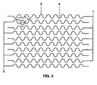
- Figure 5 shows semicircular wave electrode paths, i. the shape of everyone Electrode corresponds to a sequence of semicircles, which alternately mirror images with respect to the longitudinal axis of the respective electrode track to each other are added such that the upwardly facing semicircular arches 3 as Maxima and the downward semicircular arches 4 are called minima can be.
- the electrode tracks can be in Figure 5 from which arise in Figure 1 by thinking that each Sine half-wave was replaced by a suitable in-phase half-rice.
- FIG. 3 is less favorable for various reasons.
- On the other hand is here, apart from the respective nose 6, in the area of extended Maxima 3 and Minima 4 no further distinct location dependency the discharge conditions, therefore, this structure for power control initially poorly suited.
- this could be through other measures than by a variation of the discharge distance - such as in the examples of Figures 1, 2 and 4 - created such inhomogeneity be, for example, by a variation of the electrode width.
- the sawtooth shape in FIG. 4 has opposite the sinusoidal shape in FIGS and 2 again the disadvantage that through the corners 7 of the sawtooth shape also on the anode side a discharge structure - in the bipolar case of current anode side - there is a certain current concentration.
- the double sinusoidal shape shown in Figs favorable compromise with regard to the efficiency of the discharges, the Total capacity, the power control characteristics, the achievable surface luminance and the uniformity of this luminance.
- the semicircular waveform shown in FIG. 5 is distinguished from the sinusoidal shape shown in FIGS. 1 and 2 by lower gradients in the range of the control length SL, which has a positive effect on the power controllability, ie the dimming behavior. Therefore, an exemplary embodiment based on the electrode configuration shown in FIG. 5 will be explained in more detail below.
- It is a flat lamp with a discharge vessel (not shown), which is formed of a bottom and a front plate and a peripheral frame.
- the plates are made of glass of thickness 2 mm and dimensions 105 mm by 137 mm.
- the frame height and width are each 5 mm.
- the inner surface of the bottom plate is 78 mm by 110 mm.
- the electrode configuration of Figure 5 is arranged and covered with a glass solder layer (not shown) of thickness about 150 microns (two-sided dielectrically impeded discharge). Therefore, this flat lamp is also suitable for the bipolar operating method variant.
- a light-reflecting layer of Al 2 O 3 or TiO 2 is applied to the bottom plate and the frame. This is followed by a three-band phosphor layer on all inner surfaces.
- the discharge vessel is filled with xenon at a pressure of approx. 13 kPa.
- a voltage pulse frequency of 80 kHz can be with the peak voltage as a control variable, the widths of the (not shown) delta-shaped partial discharges in the range of the respective control length SL influence. In this way, when the peak voltage is increased from 1.39 kV to 1.49 kV, the average power consumption can be increased from 7 W to 10 W.
- FIG. 6 shows a schematic circuit diagram of a ballast, which is designed for the bipolar operating method variant.
- the transformer T has two primary windings, which are shown in Figure 6 with opposite winding sense.
- Each of the primary windings is electrically connected in series with an associated switching transistor T Q with its own control device SE.
- the two control devices can also be understood as two functions of a uniform control device; is to be symbolized only that the two primary windings are not clocked together, but alternately.
- the transformer T Due to the reversal of the winding between the two primary windings, the transformer T generates alternating voltage pulses of opposite polarity in the secondary circuit S when the primary windings are clocked.
- the subassembly of the primary winding W1, the switch TQ and the control device SE is doubled , wherein by the sense of winding a sign reversal is effected.
- FIG. 7 shows corresponding real measuring curves of the outer lamp voltage U L and of the lamp current I L.
- the measured external lamp voltage U L is composed of the voltage of the actual pulse and the voltage of the natural oscillation of the secondary circuit. The latter, however, has at least no decisive influence on the discharge. Rather, what is decisive are the actual voltage pulses which cause the corresponding lamp current pulses of the ignition and the back ignition and finally result in the already disclosed in WO 94/23442 active power pulse mode. Both the ignition pulses of the external lamp voltage and the lamp current pulses of the ignition and the reignition can be seen that it is a bipolar operating method.
Landscapes
- Circuit Arrangements For Discharge Lamps (AREA)
- Vessels And Coating Films For Discharge Lamps (AREA)
- Discharge Lamps And Accessories Thereof (AREA)
- Discharge Lamp (AREA)
Description
- Figur 1
- eine schematische Darstellung einer Elektrodenkonfiguration mit sinusförmigen Anoden und Kathoden;
- Figur 2
- eine Variante zu der Elektrodenkonfiguration aus Figur 1,
- Figur 3
- eine schematische Darstellung einer weiteren Elektrodenkonfiguration mit rechteckwellenförmigen Anoden und Kathoden,
- Figur 4
- eine weitere schematische Darstellung einer Elektrodenkonfiguration mit sägezahnförmigen Anoden und Kathoden,
- Figur 5
- eine weitere schematische Darstellung einer Elektrodenkonfiguration mit halbkreiswellenförmigen Anoden und Kathoden,
- Figur 6
- ein schematisches Schaltdiagramm eines Vorschaltgeräts, das für die bipolare Betriebsverfahrensvariante geeignet ist, mit Entladungslampe; und
- Figur 7
- ein Diagramm mit Meßkurven für die äußere Spannung an und den Strom durch die Entladungslampe beim Beleuchtungssystem nach Figur 6.
| Beispiel | dmin | dmax | SL |
| Figur 1 | 5 | 8 | 9 |
| Figur 2 | 5 | 6 | 6 |
| Figur 3 | 5 | 6 | 8 |
| Figur 4 | 6 | 10 | 17 |
| Figur 5 | 4 | 8 | 5 |
Claims (27)
- Entladungslampe mit einem mit einem Entladungsmedium gefüllten Entladungsgefäß, einer streifenförmigen Kathode (2) und einer streifenförmigen Anode (1) sowie einer dielektrischen Schicht zwischen zumindest der Anode (1) und dem Entladungsmedium, wobei die Anode (1) gegenüber der Kathode (2) ausgezeichnet ist,
dadurch gekennzeichnet, daß die Anode (1) mäanderförmig verläuft, so daß der Abstand zwischen der Kathode (2) und der Anode (1) durch die Mäanderform moduliert ist. - Entladungslampe nach Anspruch 1, bei der die Kathode (2) im wesentlichen gerade verläuft.
- Entladungslampe nach Anspruch 1 oder 2, bei der eine Mehrzahl Kathoden (2) und eine Mehrzahl Anoden (1) einzelstreifenweise alternierend angeordnet sind.
- Entladungslampe nach Anspruch 2 und 3, bei der die Mäanderformen von Anoden (1), die auf beiden Seiten einer Kathode (2) verlaufen, lokal gleichphasig zueinander verlaufen, so daß die Stellen minimalen Abstandes zwischen der Kathode (2) und den jeweiligen Anoden (1) entlang der Kathode (2) alternieren.
- Entladungslampe mit einem mit einem Entladungsmedium gefüllten Entladungsgefäß, einer streifenförmigen Kathode (2) und einer streifenförmigen Anode (1) sowie einer dielektrischen Schicht zwischen zumindest der Anode (1) und dem Entladungsmedium,
dadurch gekennzeichnet, daß die Kathode (2) und die Anode (1) mäanderförmig verlaufen, wobei die Mäanderformen lokal gegenphasig zueinander verlaufen, so daß der Abstand zwischen der Kathode (2) und der Anode (1) durch beide Mäanderformen moduliert ist. - Entladungslampe nach Anspruch 5, bei der eine Mehrzahl Kathoden (2) und eine Mehrzahl Anoden (1) einzelstreifenweise alternierend angeordnet sind.
- Entladungslampe nach einem der vorstehenden Ansprüche, bei der die Mäanderform(en) im wesentlichen einen Sinusverlauf hat/haben.
- Entladungslampe nach einem der vorstehenden Ansprüche, bei der die Mäanderform(en) im wesentlichen einen Sägezahnverlauf hat/haben.
- Entladungslampe nach einem der vorstehenden Ansprüche, bei der die Mäanderform(en) im wesentlichen einen Rechteckverlauf hat/haben.
- Entladungslampe nach einem der vorstehenden Ansprüche, bei der die Mäanderform(en) im wesentlichen einen halbkreiswellenförmigen Verlauf hat/haben.
- Entladungslampe nach einem der vorstehenden Ansprüche, bei der für das quantitative Verhältnis zwischen einer Differenz zwischen einer maximalen Schlagweite dmax zwischen den Elektroden (1, 2) in einer halben Periodenlänge (SL) der Mäanderform und einer minimalen Schlagweite dmin zwischen den Elektroden (1, 2) in der halben Periodenlänge (SL) zu dieser halben Periodenlänge (SL) gilt: (dmax - dmin)/SL ≤ 0,6, vorzugsweise (dmax - dmin)/SL ≤ 0,5, besonders bevorzugterweise (dmax - dmin)/SL ≤ 0,4.
- Entladungslampe nach einem der vorstehenden Ansprüche, bei der für das Verhältnis aus einer minimalen Schlagweite dmin und einer maximalen Schlagweite dmax gilt: 0,3 < dmin/dmax < 0,9, vorzugsweise 0,4 < dmin/dmax < 0,9, besonders bevorzugterweise 0,5 < dmin/dmax < 0,9.
- Entladungslampe nach einem der vorstehenden Ansprüche, bei der die Kathoden (2) Stellen (6, 7) zur lokalen Feldverstärkung aufweisen.
- Entladungslampe nach einem der vorstehenden Ansprüche, bei der Elektrodenbereiche (5) zwischen den Mäandern mit einem grobkörnigeren Leuchtstoff und die benachbarten Mäander derselben Elektrode (1, 2) mit einem feinkörnigeren Leuchtstoff beschichtet sind.
- Entladungslampe nach einem der Ansprüche 1-13, bei der Elektrodenbereiche (5) zwischen den Mäandern mit einem grobkörnigeren Leuchtstoff beschichtet und die benachbarten Mäander derselben Elektrode (1, 2) leuchtstoffrei sind.
- Entladungslampe nach einem der vorstehenden Ansprüche, bei der Elektrodenbereiche (5) zwischen den Mäandern mit einer dickeren dielektrischen Schicht und die benachbarten Mäander derselben Elektrode (1, 2) mit einer dünneren dielektrischen Schicht beschichtet sind.
- Entladungslampe nach einem der Ansprüche 1-15, bei der Elektrodenbereiche (5) zwischen den Mäandern mit einer dielektrischen Schicht beschichtet sind und die benachbarten Mäander derselben Elektrode (1, 2) frei von dieser dielektrischen Schicht sind.
- Beleuchtungssystem mit einer Entladungslampe nach einem der vorstehenden Ansprüche und
einem Vorschaltgerät, das zu einer gepulsten Wirkleistungseinkopplung in die Entladungslampe ausgelegt ist. - Beleuchtungssystem nach Anspruch 18, bei dem das Vorschaltgerät eine Leistungssteuereinrichtung zum Steuern der Leistung der Entladungslampe durch Verändern eines elektrischen Parameters der gepulsten Wirkleistungseinkopplung in die Entladungslampe aufweist.
- Beleuchtungssystem nach Anspruch 18 oder 19, bei dem das Vorschaltgerät zu einer unipolaren Wirkleistungseinkopplung ausgelegt ist.
- Beleuchtungssystem nach einem der Ansprüche 18-20, bei dem das Vorschaltgerät ein Flußwandler ist zum Einprägen eines äußeren Spannungspulses aus einem Primärkreis über einen Transformator in einen Sekundärkreis mit der Entladungslampe, um in der Entladungslampe eine Zündung und eine innere Gegenpolarisation zu bewirken, und eine Schalteinrichtung aufweist, die ausgelegt ist zum nach der Zündung Unterbrechen des primärseitigen Stromflusses durch den Transformator zum Isolieren des Sekundärkreises, um eine Schwingung des Sekundärkreises zu erlauben, um die die äußere Spannung an der Entladungslampe bewirkende Ladung abzuziehen und durch die innere Gegenpolarisation in der Entladungslampe zu einer Rückzündung zu führen.
- Beleuchtungssystem nach einem der Ansprüche 18-20, bei dem das Vorschaltgerät ein kombinierter Sperrwandler/Flußwandler ist und eine Schalteinrichtung in einem Primärkreis aufweist, die ausgelegt ist zum Unterbrechen des primärkreisseitigen Stromflusses durch einen Transformator zum Einprägen eines äußeren Spannungspulses in einen Sekundärkreis mit der Entladungslampe, um in der Entladungslampe eine Zündung und eine Gegenpolarisation zu bewirken, und zum dann Wiedereinschalten des primärkreisseitigen Stromflusses durch den Transformator, um durch einen Gegenspannungspuls die die äußere Spannung an der Entladungslampe bewirkende Ladung von der Entladungslampe abzuziehen, um mit Hilfe der inneren Gegenpolarisation in der Entladungslampe eine Rückzündung zu bewirken.
- Beleuchtungssystem nach Anspruch 18 oder 19, bei dem das Vorschaltgerät einen leistungsversorgten Primärkreis (P), einen die Entladungslampe (L) enthaltenden Sekundärkreis (S) sowie einen den Primärkreis (P) mit dem Sekundärkreis (S) verbindenden Transformator (T) umfaßt, wobei das Vorschaltgerät dazu ausgelegt ist, an die Entladungslampe (L) äußere Spannungen (UL) mit von Spannungspuls zu Spannungspuls alternierendem Vorzeichen anzulegen.
- Beleuchtungssystem nach Anspruch 23, bei dem die Richtung des primärkreisseitigen Stromes (IW1) in dem Transformator (T) von Spannungspuls zu Spannungspuls alterniert.
- Beleuchtungssystem nach Anspruch 24, bei dem der Transformator zwei primärkreisseitige Wicklungen (W1) aufweist, die jeweils einer der beiden Stromrichtungen zugeordnet sind.
- Beleuchtungssystem nach Anspruch 25, bei dem der Primärkreis zwei Schalter (TQ) aufweist, die jeweils den Strom durch eine der beiden Wicklungen (W1) takten.
- Beleuchtungssystem nach einem der Ansprüche 18-26, bei dem der Primärkreis aus einer Wechselstromquelle versorgt wird, die zwei Speicherkondensatoren halbperiodenweise alternierend lädt, wobei jeder Speicherkondensator jeweils einer der beiden Stromrichtungen zugeordnet ist.
Applications Claiming Priority (3)
| Application Number | Priority Date | Filing Date | Title |
|---|---|---|---|
| DE19844721 | 1998-09-29 | ||
| DE19844721A DE19844721A1 (de) | 1998-09-29 | 1998-09-29 | Entladungslampe für dielektrisch behinderte Entladungen mit verbesserter Elektrodenkonfiguration |
| PCT/DE1999/002899 WO2000019487A1 (de) | 1998-09-29 | 1999-09-13 | Entladungslampe für dielektrisch behinderte entladungen mit verbesserter elektrodenkonfiguration |
Publications (2)
| Publication Number | Publication Date |
|---|---|
| EP1118101A1 EP1118101A1 (de) | 2001-07-25 |
| EP1118101B1 true EP1118101B1 (de) | 2005-04-20 |
Family
ID=7882703
Family Applications (1)
| Application Number | Title | Priority Date | Filing Date |
|---|---|---|---|
| EP99969838A Expired - Lifetime EP1118101B1 (de) | 1998-09-29 | 1999-09-13 | Entladungslampe für dielektrisch behinderte entladungen mit verbesserter elektrodenkonfiguration |
Country Status (11)
| Country | Link |
|---|---|
| US (1) | US6411039B1 (de) |
| EP (1) | EP1118101B1 (de) |
| JP (1) | JP4650977B2 (de) |
| KR (1) | KR100456350B1 (de) |
| CN (1) | CN1165954C (de) |
| AT (1) | ATE293841T1 (de) |
| CA (1) | CA2345684C (de) |
| DE (2) | DE19844721A1 (de) |
| HU (1) | HUP0105135A3 (de) |
| TW (1) | TW483289B (de) |
| WO (1) | WO2000019487A1 (de) |
Families Citing this family (14)
| Publication number | Priority date | Publication date | Assignee | Title |
|---|---|---|---|---|
| DE19845228A1 (de) * | 1998-10-01 | 2000-04-27 | Patent Treuhand Ges Fuer Elektrische Gluehlampen Mbh | Dimmbare Entladungslampe für dielektrisch behinderte Entladungen |
| DE10011484A1 (de) * | 2000-03-09 | 2001-09-13 | Patent Treuhand Ges Fuer Elektrische Gluehlampen Mbh | Verbessertes Pulsbetriebsverfahren für eine Stille Entladungslampe |
| DE10026781C1 (de) * | 2000-05-31 | 2002-01-24 | Heraeus Noblelight Gmbh | Entladungslampe für dielektrisch behinderte Entladung |
| DE10048187A1 (de) * | 2000-09-28 | 2002-04-11 | Patent Treuhand Ges Fuer Elektrische Gluehlampen Mbh | Entladungslampe für dielektrisch behinderte Entladungen mit Stützelementen zwischen einer Bodenplatte und einer Deckenplatte |
| DE10063930C1 (de) * | 2000-12-20 | 2002-08-01 | Patent Treuhand Ges Fuer Elektrische Gluehlampen Mbh | Stille Entladungslampe mit steuerbarer Farbe und Bildanzeigeeinrichtung mit dieser stillen Entladungslampe sowie Verfahren zum Betreiben derselben |
| DE10310144A1 (de) * | 2003-03-07 | 2004-09-16 | Patent-Treuhand-Gesellschaft für elektrische Glühlampen mbH | Entladungslampe für dielektrisch behinderte Entladungen mit zurückspringend überhändenden Entladungselektrodenabschnitten |
| JP4112449B2 (ja) * | 2003-07-28 | 2008-07-02 | 株式会社東芝 | 放電電極及び放電灯 |
| DE10347636A1 (de) * | 2003-10-09 | 2005-05-04 | Patent Treuhand Ges Fuer Elektrische Gluehlampen Mbh | Entladungslampe mit mindestens einer Außenelektrode und Verfahren zu ihrer Herstellung |
| JP2005339955A (ja) * | 2004-05-26 | 2005-12-08 | Harison Toshiba Lighting Corp | 平面型放電ランプ及び照明装置 |
| DE102004055328B3 (de) * | 2004-11-16 | 2006-04-13 | Institut für Niedertemperatur-Plasmaphysik e.V. | Vorrichtung nach dem Prinzip einer dielektrisch behinderten Entladung zur Strahlungserzeugung |
| US20060175973A1 (en) * | 2005-02-07 | 2006-08-10 | Lisitsyn Igor V | Xenon lamp |
| DE102005046481A1 (de) * | 2005-09-28 | 2007-03-29 | Patent-Treuhand-Gesellschaft für elektrische Glühlampen mbH | Entladungslampe für dielektrisch behinderte Entladungen mit Boden- und Deckenplatte und Stützelementen dazwischen |
| DE102006026332A1 (de) | 2006-06-02 | 2007-12-06 | Patent-Treuhand-Gesellschaft für elektrische Glühlampen mbH | Entladungslampe für dielektrisch behinderte Entladungen mit rippenartigen Stützelementen zwischen Bodenplatte und Deckenplatte |
| DE102006026333A1 (de) | 2006-06-02 | 2007-12-06 | Patent-Treuhand-Gesellschaft für elektrische Glühlampen mbH | Entladungslampe für dielektrisch behinderte Entladungen mit flachem Entladungsgefäß |
Family Cites Families (14)
| Publication number | Priority date | Publication date | Assignee | Title |
|---|---|---|---|---|
| US4185229A (en) | 1976-07-02 | 1980-01-22 | Fujitsu Limited | Gas discharge panel |
| JPS60130033A (ja) * | 1983-12-16 | 1985-07-11 | Sony Corp | 陰極線管の内蔵抵抗器 |
| JPH02189854A (ja) * | 1989-01-17 | 1990-07-25 | Toshiba Lighting & Technol Corp | 希ガス放電灯 |
| DE4311197A1 (de) | 1993-04-05 | 1994-10-06 | Patent Treuhand Ges Fuer Elektrische Gluehlampen Mbh | Verfahren zum Betreiben einer inkohärent strahlenden Lichtquelle |
| US5760541A (en) * | 1996-02-26 | 1998-06-02 | Hewlett-Packard Company | Electrode for external electrode fluorescent lamp providing improved longitudinal stability of intensity striations |
| DE19628770A1 (de) * | 1996-07-17 | 1998-01-22 | Bosch Gmbh Robert | Verfahren zur Beeinflussung der Leistungsabgabe eines Verstärkerelementes sowie Anordnung |
| DE19636965B4 (de) * | 1996-09-11 | 2004-07-01 | Patent-Treuhand-Gesellschaft für elektrische Glühlampen mbH | Elektrische Strahlungsquelle und Bestrahlungssystem mit dieser Strahlungsquelle |
| TW412770B (en) | 1997-03-21 | 2000-11-21 | Patent Treuhand Ges Fuer Elektrische Gluehlampen Mbh | Flat fluorescent lamp for background lighting and a liquid crystal display device having this flat fluorescent lamp |
| ES2201499T3 (es) * | 1997-03-21 | 2004-03-16 | Patent-Treuhand-Gesellschaft Fur Elektrische Gluhlampen Mbh | Lampara de descarga gaseosa con electrodos dielectricamente inhibidos. |
| JPH1131480A (ja) * | 1997-05-12 | 1999-02-02 | Toshiba Lighting & Technol Corp | 誘電体バリヤ放電ランプ用放電体、誘電体バリヤ放電ランプ、誘電体バリヤ放電ランプ装置および紫外線照射装置 |
| DE19839329A1 (de) | 1998-08-28 | 2000-03-09 | Patent Treuhand Ges Fuer Elektrische Gluehlampen Mbh | Elektronisches Vorschaltgerät für Entladungslampe mit dielektrisch behinderten Entladungen |
| DE19839336A1 (de) | 1998-08-28 | 2000-03-09 | Patent Treuhand Ges Fuer Elektrische Gluehlampen Mbh | Elektronisches Vorschaltgerät für Entladungslampe mit dielektrisch behinderten Entladungen |
| DE19843419A1 (de) * | 1998-09-22 | 2000-03-23 | Patent Treuhand Ges Fuer Elektrische Gluehlampen Mbh | Entladungslampe mit dielektrisch behinderten Elektroden |
| DE19844720A1 (de) * | 1998-09-29 | 2000-04-06 | Patent Treuhand Ges Fuer Elektrische Gluehlampen Mbh | Dimmbare Entladungslampe für dielektrisch behinderte Entladungen |
-
1998
- 1998-09-29 DE DE19844721A patent/DE19844721A1/de not_active Withdrawn
-
1999
- 1999-08-18 TW TW088114094A patent/TW483289B/zh not_active IP Right Cessation
- 1999-09-13 US US09/787,721 patent/US6411039B1/en not_active Expired - Fee Related
- 1999-09-13 AT AT99969838T patent/ATE293841T1/de not_active IP Right Cessation
- 1999-09-13 CN CNB998115371A patent/CN1165954C/zh not_active Expired - Fee Related
- 1999-09-13 DE DE59911954T patent/DE59911954D1/de not_active Expired - Lifetime
- 1999-09-13 HU HU0105135A patent/HUP0105135A3/hu unknown
- 1999-09-13 EP EP99969838A patent/EP1118101B1/de not_active Expired - Lifetime
- 1999-09-13 CA CA002345684A patent/CA2345684C/en not_active Expired - Fee Related
- 1999-09-13 JP JP2000572897A patent/JP4650977B2/ja not_active Expired - Fee Related
- 1999-09-13 WO PCT/DE1999/002899 patent/WO2000019487A1/de not_active Ceased
- 1999-09-13 KR KR10-2001-7003955A patent/KR100456350B1/ko not_active Expired - Fee Related
Also Published As
| Publication number | Publication date |
|---|---|
| KR100456350B1 (ko) | 2004-11-09 |
| US6411039B1 (en) | 2002-06-25 |
| ATE293841T1 (de) | 2005-05-15 |
| WO2000019487A1 (de) | 2000-04-06 |
| DE19844721A1 (de) | 2000-04-27 |
| DE59911954D1 (de) | 2005-05-25 |
| JP4650977B2 (ja) | 2011-03-16 |
| CN1320271A (zh) | 2001-10-31 |
| EP1118101A1 (de) | 2001-07-25 |
| JP2002526895A (ja) | 2002-08-20 |
| KR20010075425A (ko) | 2001-08-09 |
| HUP0105135A2 (hu) | 2002-04-29 |
| HUP0105135A3 (en) | 2002-05-28 |
| CN1165954C (zh) | 2004-09-08 |
| CA2345684A1 (en) | 2000-04-06 |
| CA2345684C (en) | 2008-11-04 |
| TW483289B (en) | 2002-04-11 |
Similar Documents
| Publication | Publication Date | Title |
|---|---|---|
| DE19718395C1 (de) | Leuchtstofflampe und Verfahren zu ihrem Betrieb | |
| EP0912991B1 (de) | Flachleuchtstofflampe für die hintergrundbeleuchtung und flüssigkristallanzeige-vorrichtung mit dieser flachleuchtstofflampe | |
| EP0912990B1 (de) | Gasentladungslampe mit dielektrisch behinderten elektroden | |
| EP1118101A1 (de) | Entladungslampe für dielektrisch behinderte entladungen mit verbesserter elektrodenkonfiguration | |
| EP0895653A1 (de) | Elektrische strahlungsquelle und bestrahlungssystem mit dieser strahlungsquelle | |
| EP1118100B1 (de) | Dimmbare entladungslampe für dielektrisch behinderte entladungen | |
| DE19526211A1 (de) | Verfahren zum Betreiben von Entladungslampen bzw. -strahler | |
| EP0912992B1 (de) | Flachstrahler | |
| EP0901687B1 (de) | Flachstrahler | |
| EP1050066B1 (de) | Entladungslampe mit dielektrisch behinderten elektroden | |
| EP1177711A1 (de) | Verbessertes pulsbetriebsverfahren für eine stille entladungslampe | |
| EP1118099B1 (de) | Dimmbare entladungslampe für dielektrisch behinderte entladungen | |
| EP1417699B1 (de) | Entladungslampe mit zündhilfe | |
| DE19817475B4 (de) | Entladungslampe mit dielektrisch behinderten Elektroden sowie Beleuchtungssystem mit einer solchen Entladungslampe | |
| WO2000013472A2 (de) | Elektronisches vorschaltgerät für entladungslampe mit dielektrisch behinderten entladungen | |
| DE2121344A1 (de) | Wickelkondensator | |
| DE69508176T2 (de) | Piezoelektrischer Transformator mit grosser Konvertierungsfähigkeit | |
| EP1243165B1 (de) | Schaltungsanordnung zum betreiben einer gasentladungslampe | |
| EP1455381B1 (de) | Entladungslampe für dielektrisch behinderte Entladungen mit überhängenden Entladungselektrodenabschnitten | |
| EP1320869B1 (de) | Entladungslampe mit kapazitiver feldmodulation | |
| DE2642751C3 (de) | Vorrichtung zur Erzeugung von Ozon | |
| DE102005007727A1 (de) | Flache fluoreszierende Lampe für Displayvorrichtungen | |
| DE60309599T2 (de) | Plasmabildschirm mit koplanaren elektroden konstanter breite | |
| EP1306862A1 (de) | Folie für einen Folienkondensator und Folienkondensator | |
| DE102004056304A1 (de) | Beleuchtungsanordung mit einer Leuchtstofflampe, insbesondere einer Kaltkathodenlampe |
Legal Events
| Date | Code | Title | Description |
|---|---|---|---|
| PUAI | Public reference made under article 153(3) epc to a published international application that has entered the european phase |
Free format text: ORIGINAL CODE: 0009012 |
|
| 17P | Request for examination filed |
Effective date: 20010405 |
|
| AK | Designated contracting states |
Kind code of ref document: A1 Designated state(s): AT BE CH CY DE DK ES FI FR GB GR IE IT LI LU MC NL PT SE |
|
| RBV | Designated contracting states (corrected) |
Designated state(s): AT BE CH DE FI FR GB IT LI NL |
|
| GRAP | Despatch of communication of intention to grant a patent |
Free format text: ORIGINAL CODE: EPIDOSNIGR1 |
|
| GRAS | Grant fee paid |
Free format text: ORIGINAL CODE: EPIDOSNIGR3 |
|
| GRAA | (expected) grant |
Free format text: ORIGINAL CODE: 0009210 |
|
| AK | Designated contracting states |
Kind code of ref document: B1 Designated state(s): AT BE CH DE FI FR GB IT LI NL |
|
| REG | Reference to a national code |
Ref country code: GB Ref legal event code: FG4D Free format text: NOT ENGLISH |
|
| REG | Reference to a national code |
Ref country code: CH Ref legal event code: EP |
|
| REG | Reference to a national code |
Ref country code: CH Ref legal event code: NV Representative=s name: SIEMENS SCHWEIZ AG |
|
| REG | Reference to a national code |
Ref country code: IE Ref legal event code: FG4D Free format text: LANGUAGE OF EP DOCUMENT: GERMAN |
|
| REF | Corresponds to: |
Ref document number: 59911954 Country of ref document: DE Date of ref document: 20050525 Kind code of ref document: P |
|
| GBT | Gb: translation of ep patent filed (gb section 77(6)(a)/1977) |
Effective date: 20050607 |
|
| PLBE | No opposition filed within time limit |
Free format text: ORIGINAL CODE: 0009261 |
|
| STAA | Information on the status of an ep patent application or granted ep patent |
Free format text: STATUS: NO OPPOSITION FILED WITHIN TIME LIMIT |
|
| ET | Fr: translation filed | ||
| 26N | No opposition filed |
Effective date: 20060123 |
|
| REG | Reference to a national code |
Ref country code: CH Ref legal event code: PCAR Free format text: SIEMENS SCHWEIZ AG;INTELLECTUAL PROPERTY FREILAGERSTRASSE 40;8047 ZUERICH (CH) |
|
| PGFP | Annual fee paid to national office [announced via postgrant information from national office to epo] |
Ref country code: NL Payment date: 20090915 Year of fee payment: 11 Ref country code: FI Payment date: 20090908 Year of fee payment: 11 Ref country code: AT Payment date: 20090813 Year of fee payment: 11 |
|
| PGFP | Annual fee paid to national office [announced via postgrant information from national office to epo] |
Ref country code: CH Payment date: 20091208 Year of fee payment: 11 |
|
| PGFP | Annual fee paid to national office [announced via postgrant information from national office to epo] |
Ref country code: BE Payment date: 20090916 Year of fee payment: 11 |
|
| BERE | Be: lapsed |
Owner name: *PATENT-TREUHAND-G.- FUR ELEKTRISCHE GLUHLAMPEN M. Effective date: 20100930 |
|
| REG | Reference to a national code |
Ref country code: NL Ref legal event code: V1 Effective date: 20110401 |
|
| REG | Reference to a national code |
Ref country code: CH Ref legal event code: PL |
|
| PG25 | Lapsed in a contracting state [announced via postgrant information from national office to epo] |
Ref country code: FI Free format text: LAPSE BECAUSE OF NON-PAYMENT OF DUE FEES Effective date: 20100913 |
|
| PG25 | Lapsed in a contracting state [announced via postgrant information from national office to epo] |
Ref country code: BE Free format text: LAPSE BECAUSE OF NON-PAYMENT OF DUE FEES Effective date: 20100930 Ref country code: CH Free format text: LAPSE BECAUSE OF NON-PAYMENT OF DUE FEES Effective date: 20100930 Ref country code: LI Free format text: LAPSE BECAUSE OF NON-PAYMENT OF DUE FEES Effective date: 20100930 |
|
| PG25 | Lapsed in a contracting state [announced via postgrant information from national office to epo] |
Ref country code: AT Free format text: LAPSE BECAUSE OF NON-PAYMENT OF DUE FEES Effective date: 20100913 Ref country code: NL Free format text: LAPSE BECAUSE OF NON-PAYMENT OF DUE FEES Effective date: 20110401 |
|
| REG | Reference to a national code |
Ref country code: DE Ref legal event code: R081 Ref document number: 59911954 Country of ref document: DE Owner name: OSRAM GMBH, DE Free format text: FORMER OWNER: OSRAM GESELLSCHAFT MIT BESCHRAENKTER HAFTUNG, 81543 MUENCHEN, DE Effective date: 20111130 |
|
| PGFP | Annual fee paid to national office [announced via postgrant information from national office to epo] |
Ref country code: GB Payment date: 20120917 Year of fee payment: 14 |
|
| PGFP | Annual fee paid to national office [announced via postgrant information from national office to epo] |
Ref country code: IT Payment date: 20120927 Year of fee payment: 14 Ref country code: FR Payment date: 20121002 Year of fee payment: 14 |
|
| PGFP | Annual fee paid to national office [announced via postgrant information from national office to epo] |
Ref country code: DE Payment date: 20121023 Year of fee payment: 14 |
|
| REG | Reference to a national code |
Ref country code: DE Ref legal event code: R081 Ref document number: 59911954 Country of ref document: DE Owner name: OSRAM GMBH, DE Free format text: FORMER OWNER: OSRAM AG, 81543 MUENCHEN, DE Effective date: 20130205 |
|
| REG | Reference to a national code |
Ref country code: DE Ref legal event code: R081 Ref document number: 59911954 Country of ref document: DE Owner name: OSRAM GMBH, DE Free format text: FORMER OWNER: OSRAM GMBH, 81543 MUENCHEN, DE Effective date: 20130822 |
|
| GBPC | Gb: european patent ceased through non-payment of renewal fee |
Effective date: 20130913 |
|
| REG | Reference to a national code |
Ref country code: DE Ref legal event code: R119 Ref document number: 59911954 Country of ref document: DE Effective date: 20140401 |
|
| REG | Reference to a national code |
Ref country code: FR Ref legal event code: ST Effective date: 20140530 |
|
| PG25 | Lapsed in a contracting state [announced via postgrant information from national office to epo] |
Ref country code: GB Free format text: LAPSE BECAUSE OF NON-PAYMENT OF DUE FEES Effective date: 20130913 |
|
| PG25 | Lapsed in a contracting state [announced via postgrant information from national office to epo] |
Ref country code: FR Free format text: LAPSE BECAUSE OF NON-PAYMENT OF DUE FEES Effective date: 20130930 Ref country code: DE Free format text: LAPSE BECAUSE OF NON-PAYMENT OF DUE FEES Effective date: 20140401 Ref country code: IT Free format text: LAPSE BECAUSE OF NON-PAYMENT OF DUE FEES Effective date: 20130913 |