EP1119057A2 - Lichtdurchlässige Elektrode, Strukturierungsverfahren und Herstellungsverfahren eines, diese Elektrode anwendenden, Halbleiterbauelements - Google Patents
Lichtdurchlässige Elektrode, Strukturierungsverfahren und Herstellungsverfahren eines, diese Elektrode anwendenden, Halbleiterbauelements Download PDFInfo
- Publication number
- EP1119057A2 EP1119057A2 EP01100513A EP01100513A EP1119057A2 EP 1119057 A2 EP1119057 A2 EP 1119057A2 EP 01100513 A EP01100513 A EP 01100513A EP 01100513 A EP01100513 A EP 01100513A EP 1119057 A2 EP1119057 A2 EP 1119057A2
- Authority
- EP
- European Patent Office
- Prior art keywords
- film
- transparent electrode
- zno
- zno film
- transparent
- Prior art date
- Legal status (The legal status is an assumption and is not a legal conclusion. Google has not performed a legal analysis and makes no representation as to the accuracy of the status listed.)
- Withdrawn
Links
- 238000000059 patterning Methods 0.000 title claims abstract description 50
- 238000000034 method Methods 0.000 title claims abstract description 41
- 239000004065 semiconductor Substances 0.000 title claims description 22
- 238000004519 manufacturing process Methods 0.000 title claims description 17
- 239000000758 substrate Substances 0.000 claims abstract description 62
- 239000010408 film Substances 0.000 claims description 340
- 238000006243 chemical reaction Methods 0.000 claims description 87
- 239000011521 glass Substances 0.000 claims description 49
- 238000002844 melting Methods 0.000 claims description 40
- 230000008018 melting Effects 0.000 claims description 40
- IJGRMHOSHXDMSA-UHFFFAOYSA-N Atomic nitrogen Chemical compound N#N IJGRMHOSHXDMSA-UHFFFAOYSA-N 0.000 claims description 20
- 229910052751 metal Inorganic materials 0.000 claims description 20
- 239000002184 metal Substances 0.000 claims description 20
- 239000010409 thin film Substances 0.000 claims description 18
- XAGFODPZIPBFFR-UHFFFAOYSA-N aluminium Chemical compound [Al] XAGFODPZIPBFFR-UHFFFAOYSA-N 0.000 claims description 10
- 229910052757 nitrogen Inorganic materials 0.000 claims description 10
- 229910052782 aluminium Inorganic materials 0.000 claims description 9
- 229910052709 silver Inorganic materials 0.000 claims description 8
- 239000004332 silver Substances 0.000 claims description 7
- 239000012299 nitrogen atmosphere Substances 0.000 claims description 3
- 230000001678 irradiating effect Effects 0.000 claims description 2
- 238000004544 sputter deposition Methods 0.000 abstract description 11
- 238000009413 insulation Methods 0.000 abstract description 3
- XLOMVQKBTHCTTD-UHFFFAOYSA-N Zinc monoxide Chemical compound [Zn]=O XLOMVQKBTHCTTD-UHFFFAOYSA-N 0.000 description 333
- 239000011787 zinc oxide Substances 0.000 description 166
- 238000009826 distribution Methods 0.000 description 13
- 239000000463 material Substances 0.000 description 12
- 238000003475 lamination Methods 0.000 description 11
- 238000004088 simulation Methods 0.000 description 11
- XOLBLPGZBRYERU-UHFFFAOYSA-N tin dioxide Chemical compound O=[Sn]=O XOLBLPGZBRYERU-UHFFFAOYSA-N 0.000 description 11
- 238000010030 laminating Methods 0.000 description 8
- 229910021417 amorphous silicon Inorganic materials 0.000 description 6
- 230000015556 catabolic process Effects 0.000 description 5
- 238000006731 degradation reaction Methods 0.000 description 5
- 230000000694 effects Effects 0.000 description 5
- 238000002347 injection Methods 0.000 description 5
- 239000007924 injection Substances 0.000 description 5
- 238000000926 separation method Methods 0.000 description 5
- BQCADISMDOOEFD-UHFFFAOYSA-N Silver Chemical compound [Ag] BQCADISMDOOEFD-UHFFFAOYSA-N 0.000 description 4
- 239000012298 atmosphere Substances 0.000 description 4
- 238000010586 diagram Methods 0.000 description 4
- 230000001629 suppression Effects 0.000 description 4
- 238000010521 absorption reaction Methods 0.000 description 3
- 238000009792 diffusion process Methods 0.000 description 3
- 230000007774 longterm Effects 0.000 description 3
- 230000003287 optical effect Effects 0.000 description 3
- GYHNNYVSQQEPJS-UHFFFAOYSA-N Gallium Chemical compound [Ga] GYHNNYVSQQEPJS-UHFFFAOYSA-N 0.000 description 2
- 229910008556 Li2O—Al2O3—SiO2 Inorganic materials 0.000 description 2
- 229910000611 Zinc aluminium Inorganic materials 0.000 description 2
- 238000010292 electrical insulation Methods 0.000 description 2
- 229910052733 gallium Inorganic materials 0.000 description 2
- 230000000149 penetrating effect Effects 0.000 description 2
- 230000000717 retained effect Effects 0.000 description 2
- HBMJWWWQQXIZIP-UHFFFAOYSA-N silicon carbide Chemical compound [Si+]#[C-] HBMJWWWQQXIZIP-UHFFFAOYSA-N 0.000 description 2
- 239000007787 solid Substances 0.000 description 2
- LEVVHYCKPQWKOP-UHFFFAOYSA-N [Si].[Ge] Chemical compound [Si].[Ge] LEVVHYCKPQWKOP-UHFFFAOYSA-N 0.000 description 1
- 230000005540 biological transmission Effects 0.000 description 1
- 239000004020 conductor Substances 0.000 description 1
- 230000007812 deficiency Effects 0.000 description 1
- 230000002950 deficient Effects 0.000 description 1
- 230000000593 degrading effect Effects 0.000 description 1
- 238000002474 experimental method Methods 0.000 description 1
- AMGQUBHHOARCQH-UHFFFAOYSA-N indium;oxotin Chemical compound [In].[Sn]=O AMGQUBHHOARCQH-UHFFFAOYSA-N 0.000 description 1
- 239000004973 liquid crystal related substance Substances 0.000 description 1
- 238000005259 measurement Methods 0.000 description 1
- 238000012986 modification Methods 0.000 description 1
- 230000004048 modification Effects 0.000 description 1
- 230000035515 penetration Effects 0.000 description 1
- 230000002093 peripheral effect Effects 0.000 description 1
- 238000005268 plasma chemical vapour deposition Methods 0.000 description 1
- 229910001887 tin oxide Inorganic materials 0.000 description 1
Images


Classifications
-
- H—ELECTRICITY
- H10—SEMICONDUCTOR DEVICES; ELECTRIC SOLID-STATE DEVICES NOT OTHERWISE PROVIDED FOR
- H10F—INORGANIC SEMICONDUCTOR DEVICES SENSITIVE TO INFRARED RADIATION, LIGHT, ELECTROMAGNETIC RADIATION OF SHORTER WAVELENGTH OR CORPUSCULAR RADIATION
- H10F71/00—Manufacture or treatment of devices covered by this subclass
- H10F71/125—The active layers comprising only Group II-VI materials, e.g. CdS, ZnS or CdTe
-
- H—ELECTRICITY
- H10—SEMICONDUCTOR DEVICES; ELECTRIC SOLID-STATE DEVICES NOT OTHERWISE PROVIDED FOR
- H10F—INORGANIC SEMICONDUCTOR DEVICES SENSITIVE TO INFRARED RADIATION, LIGHT, ELECTROMAGNETIC RADIATION OF SHORTER WAVELENGTH OR CORPUSCULAR RADIATION
- H10F77/00—Constructional details of devices covered by this subclass
- H10F77/20—Electrodes
- H10F77/206—Electrodes for devices having potential barriers
- H10F77/211—Electrodes for devices having potential barriers for photovoltaic cells
-
- H—ELECTRICITY
- H10—SEMICONDUCTOR DEVICES; ELECTRIC SOLID-STATE DEVICES NOT OTHERWISE PROVIDED FOR
- H10K—ORGANIC ELECTRIC SOLID-STATE DEVICES
- H10K50/00—Organic light-emitting devices
- H10K50/80—Constructional details
- H10K50/805—Electrodes
- H10K50/81—Anodes
- H10K50/816—Multilayers, e.g. transparent multilayers
-
- Y—GENERAL TAGGING OF NEW TECHNOLOGICAL DEVELOPMENTS; GENERAL TAGGING OF CROSS-SECTIONAL TECHNOLOGIES SPANNING OVER SEVERAL SECTIONS OF THE IPC; TECHNICAL SUBJECTS COVERED BY FORMER USPC CROSS-REFERENCE ART COLLECTIONS [XRACs] AND DIGESTS
- Y02—TECHNOLOGIES OR APPLICATIONS FOR MITIGATION OR ADAPTATION AGAINST CLIMATE CHANGE
- Y02E—REDUCTION OF GREENHOUSE GAS [GHG] EMISSIONS, RELATED TO ENERGY GENERATION, TRANSMISSION OR DISTRIBUTION
- Y02E10/00—Energy generation through renewable energy sources
- Y02E10/50—Photovoltaic [PV] energy
- Y02E10/543—Solar cells from Group II-VI materials
-
- Y—GENERAL TAGGING OF NEW TECHNOLOGICAL DEVELOPMENTS; GENERAL TAGGING OF CROSS-SECTIONAL TECHNOLOGIES SPANNING OVER SEVERAL SECTIONS OF THE IPC; TECHNICAL SUBJECTS COVERED BY FORMER USPC CROSS-REFERENCE ART COLLECTIONS [XRACs] AND DIGESTS
- Y02—TECHNOLOGIES OR APPLICATIONS FOR MITIGATION OR ADAPTATION AGAINST CLIMATE CHANGE
- Y02P—CLIMATE CHANGE MITIGATION TECHNOLOGIES IN THE PRODUCTION OR PROCESSING OF GOODS
- Y02P70/00—Climate change mitigation technologies in the production process for final industrial or consumer products
- Y02P70/50—Manufacturing or production processes characterised by the final manufactured product
Definitions
- This invention relates to a transparent electrode, a patterning method for the same, and a manufacturing method for a semiconductor element of the same formed on a transparent substrate used in an integrated type photovoltaic device, a liquid crystal display device, and an organic EL device or the like.
- a photovoltaic device comprising an amorphous semiconductor of amorphous silicon, amorphous silicon carbide, amorphous silicon germanium or the like has been developed as a solar cell device because it is manufactured at low cost and easily increases in size.
- a photovoltaic element 100 of an amorphous semiconductor is formed by laminating a transparent electrode 102, a photovoltaic conversion layer 103 of a lamination of p-, i-, and n-type amorphous semiconductor layers 103p, 103i, 103n, and a rear surface metal electrode 104 in this order on a glass substrate 101.
- Tin oxide (SnO 2 ) and ITO (Indium Tin Oxide) are used conventionally as transparent conductive material for forming the transparent electrode 102.
- ITO Indium Tin Oxide
- ZnO zinc oxide
- a photovoltaic element using ZnO is manufactured by the following processes.
- a transparent electrode 102 of ZnO is formed on a glass substrate 101 by sputtering, and a photovoltaic conversion layer 103 formed of a lamination of a p-type layer 103p of approximately 150 ⁇ of p-type amorphous silicon carbide, an i-type layer 103i of approximately 4000 ⁇ of i-type amorphous silicon, and an n-type layer 103n of approximately 200 ⁇ of n-type amorphous silicon is formed by plasma CVD.
- a rear surface metal electrode 104 of silver (Ag) is sequentially laminated by sputtering to manufacture the photovoltaic element 100.
- Photovoltaic elements including transparent electrodes 102 of ZnO of various thickness are manufactured and the photovoltaic conversion efficiency of them are measured. The results are shown in Fig. 36. As shown in a characteristic diagram of Fig. 36, high photovoltaic conversion efficiency over 10.5% is obtained when a thickness of the transparent electrode 102 is approximately 2100-5000 ⁇ .
- the photovoltaic element using the transparent electrode of ZnO can provide high photovoltaic conversion efficiency.
- the photovoltaic device comprising the amorphous semiconductor has an integrated structure so as to take out a high voltage from a single substrate.
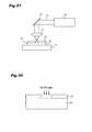
- a structure of a laser patterning device is explained by referring to Fig. 37.
- a laser 11 emitted from an Nd:YAG laser oscillating device 10 changes its direction at a reflection mirror 12, is condensed by a condensing lens 13, and irradiates a region to be processed of an object to be processed 20 mounted on a moving table 14 of an XYZ stage.
- a pattern is controlled by moving the moving table 14 with the object to be processed 20 mounted thereon.
- the transparent substrate 21 with the transparent electrode film 22 formed on the whole surface thereof as the object to be processed is mounted on the moving table 14.
- the moving table 14 is controlled to move in XYZ directions so that the region to be processed of the transparent electrode 22 is eliminated by laser as shown in Fig. 38.
- the ZnO material has moisture absorption property. Therefore, when the ZnO film is retained in an atmosphere over a day, moisture in the atmosphere penetrates from a surface of the ZnO film and solid state properties change, resulting in significant failure of laser patterning.
- Fig. 39 is results of temperature distribution simulation in laser patterning; an Nd:YAG laser (wavelength 1064nm, power 10W, a beam diameter 50 ⁇ m) is irradiated to an aluminum dope ZnO film(7500 ⁇ in thickness) formed on a glass substrate by sputtering.
- Nd:YAG laser wavelength 1064nm, power 10W, a beam diameter 50 ⁇ m
- laser energy injected to the ZnO film laser energy excluding reflection and transmission loss
- the laser-irradiated ZnO film is required to be evaporated (scattered) with the temperature reaching over the melting point and be completely eliminated so as to obtain complete electrical insulation by laser patterning.
- the ZnO film is required to melt to an interface of the glass and the ZnO film completely. In this case, a temperature of the ZnO film on a surface side reaches over the melting point and is in a high temperature state.
- the excessive energy not only is converted into kinetic energy of a ZnO molecule but also moves to a periphery of a laser irradiated part by heat conduction, resulting in following heat damages; (1) volume expansion of the laser irradiated end part, (2) a crack of the laser irradiated end part, (3) peeling of the ZnO film from the glass substrate, (4) diffusion of the ZnO forming element in the glass substrate.
- Fig. 40 is a characteristic view showing relations between a thickness of the ZnO film and yields of non-defective item having resistance between the electrodes not less than 10M ⁇ .
- a separation width of the two electrodes is approximately 100 ⁇ m as in the case of using for a photovoltaic device. It is found that high yields of over 90% can be obtained when a thickness of the ZnO film is larger than 5000 ⁇ but as a thickness becomes small, the yield declines. When the thickness is smaller than 4500 ⁇ , yields is as low as under 40%.
- the measurements show whether the film is completely separated depending on resistance between the electrodes.
- the thickness is large, as shown in Fig. 39, a temperature on a surface of the ZnO film is far higher than the melting point and deficiency particular to the ZnO film may occur. Therefore, when the ZnO film with merely a large thickness is used as a transparent electrode of the photovoltaic device, degradation of characteristics and reliability may occur.
- This invention was made to use a transparent electrode film for a photovoltaic device of a ZnO film (gallium dope ZnO and aluminum dope ZnO) film which is manufactured at low cost as compared with conventionally used SnO 2 , ITO or the like.
- this invention was made to provide a transparent electrode and a manufacturing method thereof capable of preventing phenomena (heat damages, insulation failure or the like) particular to the ZnO film appearing in a laser patterning process for forming the integrated type photovoltaic device.
- a transparent electrode according to this invention is formed by patterning a transparent electrode film formed on a transparent substrate with a laser, and comprises a transparent electrode film having a lower melting point than that of a ZnO film and the ZnO film laminated in this order on the transparent substrate.
- the transparent electrode having a lower melting point is provided on a side apart from the surface to be irradiated with a laser, thus injection of excessive laser energy higher than the melting point of the material becomes unnecessary, resulting in suppression of heat damage (volume expansion, a crack) on the end part to be irradiated with a laser.
- An ITO film may be used as a transparent electrode film having a lower melting point than that of the ZnO film.
- the melting point of the ITO film is lower than that of the ZnO film, excessive laser energy higher than the melting point of the material becomes unnecessary, resulting in suppression of heat damage of a laser irradiated end part.
- the ITO film may be 100-1000 ⁇ , and the ZnO film may be 2500-5000 ⁇ .
- the transparent electrode film having the lower melting point than that of the ZnO film is a metal thin film.
- the metal thin film may be formed of silver and is 50-300 ⁇ .
- the metal thin film is formed of aluminum and is 50-100 ⁇ .
- a moisture proof layer containing nitrogen may be formed on a surface of the ZnO film.
- the moisture proof layer prevents moisture from penetrating from a surface of the ZnO film so that workability of laser-patterning is not degraded. In addition, long-term reliability of the ZnO film is improved.
- a transparent electrode film having a lower melting point than that of a ZnO film is formed on a transparent substrate, a ZnO film is formed on the transparent electrode film, and regions to be irradiated of the transparent electrode film and the ZnO film are eliminated and patterned by laser irradiation.
- the transparent electrode having a lower melting point is provided on a side apart from the surface to be irradiated with a laser, thus injection of excessive laser energy higher than the melting point of the material becomes unnecessary, resulting in suppression of heat damage (volume expansion, a crack) on the end part to be irradiated with a laser.
- a moisture proof layer containing nitrogen is formed on a surface of the ZnO film.
- the moisture proof layer prevents moisture from penetrating from a surface of the ZnO film so that workability of laser-patterning is not degraded. In addition, long-term reliability of the ZnO film is improved.
- An ITO film as the transparent electrode film having the lower melting point than that of the ZnO film is formed by sputtering.
- the transparent substrate is a glass substrate and a crystallized glass layer is provided between the glass substrate and the ITO film.
- the crystallized glass layer prevents the ZnO component element from diffusing to the glass substrate in laser-patterning.
- the ITO film may be 100-1000 ⁇ , and the ZnO film may be 2500-5000 ⁇ .
- the transparent electrode film having the lower melting point than that of the ZnO film may be a metal thin film.
- the metal thin film is formed of silver and is 50-300 ⁇ .
- the metal thin film is formed of aluminum and is 50-100 ⁇ .
- a manufacturing method for a semiconductor element comprises a process for forming a transparent electrode film having a lower melting point than that of a ZnO film on a transparent substrate and forming a ZnO film on the transparent electrode film, a process for forming a plurality of transparent electrodes on the transparent substrate by irradiating laser on the ZnO film and eliminating and patterning regions to be irradiated of the transparent electrode film and the ZnO film, a process for forming a photovoltaic conversion layer of an amorphous semiconductor on the transparent substrate with the plurality of divided transparent electrodes included, and a process for forming a highly reflective conductive film on the photovoltaic conversion layer.
- the manufacturing method for the semiconductor element according to this invention further comprises a process for separating the previously formed photovoltaic conversion layer into a plurality of photovoltaic conversion layers by laser irradiation, and a process for dividing into a plurality of electrodes by laser irradiation to the previously formed highly reflective conductive film.
- a ZnO film (gallium doped ZnO, and aluminum dope ZnO) of lower cost material than SnO 2 and ITO or the like used conventionally is used as a transparent electrode film for a photovoltaic device according to this invention.
- Heat damage on the ZnO film in a laser patterning process for forming an integrated type photovoltaic device results from excessive injection of heat energy higher than a melting point.
- This invention provides a transparent electrode capable of laser-patterning without injecting excessive heat energy higher than the melting point.
- the transparent electrode is provided with a crystallized glass (Li 2 O-Al 2 O 3 -SiO 2 ) layer 2 on a transparent glass substrate 1, and an ITO film 3 and a ZnO film 4 are laminated on the crystallized glass 2 by sputtering.
- the ITO film has a lower melting point than that of the ZnO film.
- the ITO film having the lower melting point is provided on a side far from a surface to be irradiated with a laser, injection of excessive laser energy higher than the melting point of material becomes unnecessary and heat damage on the laser irradiated end part (volume expansion, a crack) is suppressed.
- the laser used in this embodiment is an Nd-YAG laser (a wavelength 1064nm, power 8W, a beam diameter 50 ⁇ m), and is shaped so as to have an approximately uniform energy distribution to a region to be irradiated by using an optical system shown in Fig. 2.
- An iris 16 (a round or rectangular hole) having an aperture rate of approximately 25% to an incident diameter from a center part of the laser is arranged on an optical path of a general laser having normal energy distributions, the laser passing though the iris 16 is introduced to the condensing lens 13, the laser condensed by the condensing lens 13 is irradiated to an object to be processed on the basis of the conditions of the formula (1).
- 1/a + 1/b 1/f
- a transparent electrode film of a general photovoltaic device is 5000-10000 ⁇ in thickness and temperature gradient of more than 500K occurs in the film when such the transparent electrode film is laser-patterned.
- Fig. 39 shows results of a temperature distribution simulation in forming the transparent electrode film of only the ZnO film and it is found that temperature gradient of more than 500K occurs in the conventional film.
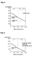
- Figs. 4, 5, 6 show results of a temperature distribution simulation of laser irradiation power optimized for each of three patterns of thickness of the aluminum dope ZnO film.
- an optimizing condition is to control a temperature of an interface of the glass and the ZnO film to be higher than a melting point 2248K.
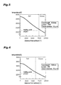
- An Nd:YaG laser in Fig. 4 has a wavelength 1064nm, power 8W, and a beam diameter 50 ⁇ m. Heat damage is not generated in Fig. 4, but is generated in Figs. 5, 6.
- An Nd:YaG laser in Fig. 5 has a wavelength 1064nm, power 10W, and a beam diameter 50 ⁇ m.
- An Nd:YaG laser in Fig. 6 has a wavelength 1064nm, power 9W, and a beam diameter 50 ⁇ m.
- a crystallized glass layer 2 of 50 ⁇ is formed on a transparent glass substrate 1, an ITO film 3 of 2500 ⁇ and a ZnO film of 5000 ⁇ are formed in this order on the crystallized glass layer 2.
- Fig. 3 shows a temperature distribution simulation of laser irradiation power in patterning with an Nd:YAG laser (a wavelength 1064nm, power 8W, a beam diameter 50 ⁇ m).
- a temperature disparity on a surface part of the ZnO film 4 or a temperature difference between the surface temperature and the melting point is within approximately 350K.
- the ITO film 3 on an interface between the crystallized glass layer 2 and the ITO film 3 has a higher temperature than the melting point and patterning is provided without heat damage.
- a thickness of the ZnO film is preferred to be not more than 5000 ⁇ in order to provide patterning without heat damage as shown in Figs. 4-6.
- the photovoltaic element using the ZnO film as the transparent electrode can obtain high photovoltaic efficiency when the thickness of the ZnO film is approximately 2100-5000 ⁇ .
- a film formed by laminating the ZnO film and other transparent electrode films is preferred to have a thickness of approximately 2100-5000 ⁇ when the ZnO is used as main material for the transparent electrode film.
- yields after divining the film by laser-patterning declines significantly when the thickness is not larger than 4500 ⁇ as shown in Fig. 40.
- a crystallized glass layer 2 of 50 ⁇ is provided on a transparent glass substrate 1, an ITO film 3 and a ZnO film 4 are formed in this order on the crystallized glass substrate 2. Thickness of each of the films is varied and patterned with an Nd:YAG laser (a wavelength 1064nm, power 8W, a beam diameter 50 ⁇ m).
- An integrated type photovoltaic device is manufactured by using this substrate. This integrated type photovoltaic device is formed as follows.
- the substrate is laser-patterned to divide into a plurality of transparent electrodes on the transparent glass substrate 1 and p-, I-, n- types amorphous semiconductor layers are laminated in this order on an approximately whole surface on the substrate 1 with the transparent electrode included, and is divided into a plurality of photovoltaic conversion layers by laser-patterning. Furthermore, a highly reflective conductive film is formed on the approximately whole surface of the substrate with the plurality of photovoltaic conversion layers and is divided into a plurality of rear surface electrodes by laser-patterning.
- a normalized release voltage and normalized conversion efficiency are measured in comparison with a photovoltaic element of 1cm 2 using the transparent electrode film of the same lamination as a reference.
- O indicates a normalized release voltage
- ⁇ indicates normalized conversion efficiency in the figures.
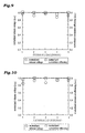
- the ZnO film of samples in Figs. 7-10 is 2500 ⁇ and the ITO film has various thickness.
- Fig. 7 is a characteristic view in measuring a normalized release voltage and normalized conversion efficiency when the ITO film is 50 ⁇ and the ZnO film is 2500 ⁇ .
- the samples are produced by laminating the ITO film of 50 ⁇ and the ZnO film of 2500 ⁇ on the glass substrate and dividing the lamination film by laser patterning of the above conditions.
- the integrated type photovoltaic device is manufactured by using these samples and a normalized release voltage and normalized release efficiency are measured.
- Fig. 8 is a characteristic view in measuring a normalized release voltage and normalized conversion efficiency when the ITO film is 100 ⁇ and the ZnO film is 2500 ⁇ .
- the samples are produced by the above described processes.
- the ITO film is 100 ⁇ and the ZnO film is 2500 ⁇
- characteristics equivalent to those of a photovoltaic element of 1cm 2 can be obtained in terms of a normalized release voltage and normalized conversion efficiency. It is found that an integrated type photovoltaic device of good characteristics is provided.
- Fig. 9 is a characteristic view in measuring a normalized release voltage and normalized conversion efficiency when the ITO film is 500 ⁇ and the ZnO film is 2500 ⁇ .
- Fig. 10 is a characteristic view in measuring a normalized release voltage and normalized conversion efficiency when the ITO film is 1000 ⁇ and the ZnO film is 2500 ⁇ .
- the samples are produced by the above described processes. As shown in Figs. 9, 10 good characteristics can be obtained as the integrated type photovoltaic device although a little degradation of characteristics is found as compared with Fig. 8.
- the ZnO film of the samples in Figs. 11-14 is 3000 ⁇ and the ITO film has various thickness.
- Fig. 11 is a characteristic view in measuring a normalized release voltage and normalized conversion efficiency when the ITO film is 50 ⁇ and the ZnO film is 3000 ⁇ .
- the samples are produced by laminating the ITO film of 50 ⁇ and the ZnO film of 3000 ⁇ in this order on the glass substrate and dividing the lamination film by laser patterning of the above conditions.
- the integrated type photovoltaic device is manufactured by using these samples and a normalized release voltage and normalized release efficiency are measured.
- Figs. 12-14 are characteristic views in measuring a normalized release voltage and normalized conversion efficiency respectively when the ITO film is 100 ⁇ and the ZnO film is 3000 ⁇ , when the ITO film is 500 ⁇ and the ZnO film is 3000 ⁇ , and when the ITO film is 1000 ⁇ and the ZnO film is 3000 ⁇ .
- the samples are produced through the above processes.
- the ZnO film of samples in Figs. 15-18 is 4000 ⁇ and the ITO film has various thickness.
- Fig. 15 is a characteristic view in measuring a normalized release voltage and normalized conversion efficiency when the ITO film is 50 ⁇ and the ZnO film is 4000 ⁇ .
- the samples are produced by laminating the ITO film of 50 ⁇ and the ZnO film of 4000 ⁇ on the glass substrate and dividing the lamination film by laser patterning of the above conditions.
- the integrated type photovoltaic device is manufactured by using these samples and a normalized release voltage and normalized release efficiency are measured.
- Figs. 16-18 are characteristic views in measuring a normalized release voltage and normalized conversion efficiency respectively when the ITO film is 100 ⁇ and the ZnO film is 4000 ⁇ , when the ITO film is 500 ⁇ and the ZnO film is 4000 ⁇ , and when the ITO film is 1000 ⁇ and the ZnO film is 4000 ⁇ .
- the samples are formed through the above processes.
- the ZnO film of samples in Figs. 19-22 is 5000 ⁇ and the ITO film has various thickness.
- Fig. 19 is a characteristic view in measuring a normalized release voltage and normalized conversion efficiency when the ITO film is 50 ⁇ and the ZnO film is 5000 ⁇ .
- the samples are produced by laminating the ITO film of 50 ⁇ and the ZnO film of 400 ⁇ on the glass substrate and dividing the lamination film by laser patterning of the above conditions.
- the integrated type photovoltaic device is manufactured by using these samples and a normalized release voltage and normalized release efficiency are measured.
- Figs. 20-22 are characteristic views in measuring a normalized release voltage and normalized conversion efficiency respectively when the ITO film is 100 ⁇ and the ZnO film is 5000 ⁇ , when the ITO film is 500 ⁇ and the ZnO film is 5000 ⁇ , and when the ITO film is 1000 ⁇ and the ZnO film is 5000 ⁇ .
- the samples are produced through the above processes.
- advantages of this invention can be obtained when the transparent electrode film having lamination of the ITO film and the ZnO film has the thickness of ITO not less than 100 ⁇ .
- the thickness of the ITO is 1000 ⁇
- the integrated type photovoltaic device of good characteristics is provided.
- the thickness of the ITO is preferred to be 100-1000 ⁇ in terms of manufacturing cost.
- the thickness of the ZnO is 2500-5000 A
- the integrated type photovoltaic device of good characteristics is provided.
- the ITO film 3 is formed by sputtering on the glass substrate 1 with the crystallized glass layer 2 formed thereon. After forming the ZnO film 4 on the ITO film 3 by sputtering, it is exposed in a nitrogen atmosphere, and a moisture proof layer containing nitrogen of a nitrogen diffused layer or an absorbing layer is formed on the surface of the ZnO film 4
- a desired moisture proof layer formed on the surface of the ZnO film 4 is exposed for different time depending on a substrate temperature.
- an atmospheric temperature is a room temperature, and an effect of the moisture proof layer is not obtained unless the film is exposed for longer than 12 hours.
- an atmospheric temperature is 100°C, and an effect of the moisture proof layer is not obtained unless the film is exposed for longer than 6 hours.
- an atmospheric temperature is 150°C, and an effect of the moisture proof layer can not appear unless the film is exposed for longer than one hours.
- normalized conversion efficiency is indicated when the photovoltaic element formed on the transparent electrode film is used as an SnO 2 surface electrode as a reference.
- the moisture proof layer prevents penetration of moisture from the surface of the ZnO film and prevents degradation of workability of laser-patterning or the like. In addition, long-term reliability of the ZnO film can be improved.
- the ITO film having a lower melting point is provided on a side far from a surface to be irradiated with a laser.
- the transparent film having a lower melting point than that of the ZnO film and having a thickness so as not to degrade the light transmittivity significantly, can provid the same effect even when any other metal thin film is used.
- silver (Ag), aluminum (Al) or the like can be used.
- a minimum and maximum value of thickness for not degrading light transmittivity and obtaining the effect of this invention are obtained experimentally. Samples are produced as in the case of the ITO film and experiments are conducted.
- a crystallized glass layer 2 of 50 ⁇ is formed on a transparent glass substrate 1, an Ag or Al film 3 and a ZnO film 4 are formed on the crystallized glass layer 2.
- a thickness of each of the layers are different in each of the different samples.
- the substrates are patterned with an Nd:YAG laser and an integrated type photovoltaic device is manufactured by using this substrate.
- a normalized release voltage and a normalized conversion efficiency are measured in comparison with a photovoltaic element of 1cm 2 using the transparent electrode film of ZnO element of 5000A.
- O indicates a normalized release voltage
- ⁇ indicates a normalized conversion efficiency.
- the samples in Figs. 27-30 have the ZnO film of 5000 ⁇ and the Ag film of different thickness.
- Fig. 27 is a characteristic view in measuring a normalized release voltage and normalized conversion efficiency when the Ag film is 30 ⁇ and the ZnO film is 5000 ⁇ . These samples are formed by laminating the Ag film of 30 ⁇ and the ZnO film of 5000 ⁇ in this order on the glass substrate and the lamination is divided by laser patterning under the above conditions. The integrated type photovoltaic device is manufactured by using these samples and a normalized release voltage and normalized release efficiency are measured.
- the normalized release voltage and normalized conversion efficiency of the sample 2 are degraded significantly, and the layers are not completely divided, resulting in occurrence of short-circuit.
- Fig. 28 is a characteristic view in measuring a normalized release voltage and normalized conversion efficiency when the Ag film is 50 ⁇ and the ZnO film is 5000 ⁇ . Samples are produced through the above processes. As shown in Fig. 28, when the Ag film is 50 ⁇ and the ZnO film is 5000 ⁇ , characteristics equivalent to those of a photovoltaic element of 1cm 2 can be obtained in terms of a normalized release voltage and normalized conversion efficiency. It is found that an integrated type photovoltaic device of good characteristics is provided.
- Fig. 29 is a characteristic view in measuring a normalized release voltage and normalized conversion efficiency when the Ag film is 200 ⁇ and the ZnO film is 5000 ⁇ .
- the samples are produced through the above processes.
- Fig. 29 when the Ag film is not less than 200 ⁇ and the ZnO film is 5000 A, characteristics equivalent to a photovoltaic element of 1cm 2 can be obtained in terms of a normalized release voltage and normalized conversion efficiency. It is found that an integrated type photovoltaic device of good characteristics is provided.
- Fig. 30 is a characteristic view in measuring a normalized release voltage and normalized conversion efficiency when the Ag film is 300 ⁇ and the ZnO film is 5000 ⁇ . Samples are produced through the above processes. As shown in Fig. 30, characteristics of the normalized conversion efficiency are degraded a little as compared with Figs. 28, 29. This seems because the thickness of the Ag film increases and light transmittivity is degraded a little. However, an integrated type photovoltaic device of good characteristics is provided in spite of a little degradation of conversion efficiency.
- the Ag film of 50-300 ⁇ , preferably 50-200 ⁇ is desirable in the transparent electrode film with the Ag film and the ZnO film laminated.
- the samples in Figs. 31-34 have a ZnO film of 5000 ⁇ and an Al film of different thickness.
- Fig. 31 is a characteristic view in measuring a normalized release voltage and normalized conversion efficiency when the Al film is 30 ⁇ and the ZnO film is 5000 ⁇ . These samples are formed by laminating the Al film of 30 ⁇ and the ZnO film of 5000 ⁇ in this order on the glass substrate and the lamination is divided by laser patterning under the above conditions. The integrated type photovoltaic device is manufactured by using these samples and a normalized release voltage and normalized release efficiency are measured.
- the normalized release voltage and normalized conversion efficiency of the sample 1, 3 are degraded significantly, and the layers are not sufficiently divided, resulting in occurrence of short-circuit.
- Fig. 32 is a characteristic view in measuring a normalized release voltage and normalized conversion efficiency when the Al film is 50 ⁇ and the ZnO film is 5000 ⁇ . Samples are produced through the above processes. As shown in Fig. 32, when the Al film is not less than 50 ⁇ and the ZnO film is 5000 ⁇ , characteristics equivalent to those of a photovoltaic element of 1cm 2 can be obtained in terms of a normalized release voltage and normalized conversion efficiency. It is found that an integrated type photovoltaic device of good characteristics is provided.
- Fig. 33 is a characteristic view in measuring a normalized release voltage and normalized conversion efficiency when the Al film is 100 ⁇ and the ZnO film is 5000 ⁇ . Samples are produced through the above processes. As shown in Fig. 33, when the Al film is not less than 100 ⁇ and the ZnO film is 5000 ⁇ , characteristics equivalent to those of a photovoltaic element of 1cm2 can be obtained in terms of a normalized release voltage and normalized conversion efficiency. It is found that an integrated type photovoltaic device of good characteristics is provided.
- Fig. 34 is a characteristic view in measuring a normalized release voltage and normalized conversion efficiency when the Al film is 150 ⁇ and the ZnO film is 5000 ⁇ . Samples are produced through the above processes. As shown in Fig. 34, characteristics of the normalized conversion efficiency are degraded a little as compared with in Figs. 32, 33. This seems because the thickness of the Al film increases and light transmittivity is degraded a little.
- the thickness of the Al film is 50-100 ⁇ in the transparent electrode film with the Al film and the ZnO film laminated.
- the transparent conductive thin film having a lower melting point than that of the ZnO film is provided on a side apart from the surface to be irradiated with a laser, thus injection of excessive laser energy higher than the melting point of the material becomes unnecessary, resulting in suppression of heat damage (volume expansion, a crack) on the end part to be irradiated with a laser.
Landscapes
- Photovoltaic Devices (AREA)
- Manufacturing Of Electric Cables (AREA)
- Electrodes Of Semiconductors (AREA)
- Non-Insulated Conductors (AREA)
Applications Claiming Priority (4)
| Application Number | Priority Date | Filing Date | Title |
|---|---|---|---|
| JP2000002141 | 2000-01-11 | ||
| JP2000002141 | 2000-01-11 | ||
| JP2000390983 | 2000-12-22 | ||
| JP2000390983A JP2001266654A (ja) | 2000-01-11 | 2000-12-22 | 透明電極及び透明電極のパターニング方法及びそれを用いた半導体素子の製造方法 |
Publications (2)
| Publication Number | Publication Date |
|---|---|
| EP1119057A2 true EP1119057A2 (de) | 2001-07-25 |
| EP1119057A3 EP1119057A3 (de) | 2005-01-05 |
Family
ID=26583285
Family Applications (1)
| Application Number | Title | Priority Date | Filing Date |
|---|---|---|---|
| EP01100513A Withdrawn EP1119057A3 (de) | 2000-01-11 | 2001-01-09 | Lichtdurchlässige Elektrode, Strukturierungsverfahren und Herstellungsverfahren eines, diese Elektrode anwendenden, Halbleiterbauelements |
Country Status (3)
| Country | Link |
|---|---|
| US (1) | US6593593B2 (de) |
| EP (1) | EP1119057A3 (de) |
| JP (1) | JP2001266654A (de) |
Cited By (4)
| Publication number | Priority date | Publication date | Assignee | Title |
|---|---|---|---|---|
| DE102007016638A1 (de) * | 2007-01-31 | 2008-08-07 | Osram Opto Semiconductors Gmbh | Verfahren zur Strukturierung elektrolumineszenter organischer Halbleiterelemente, elektrolumineszentes organisches Halbleiterelement sowie Anordnung zur Strukturierung eines solchen Elements |
| DE102009034822A1 (de) * | 2009-07-27 | 2011-02-03 | Osram Opto Semiconductors Gmbh | Elektronisches Bauelement sowie elektischer Kontakt |
| CN103952669A (zh) * | 2014-04-23 | 2014-07-30 | 北京工业大学 | 一种调控本征氧化锌薄膜可见光发光类型的方法 |
| EP3269689A4 (de) * | 2015-03-10 | 2018-11-14 | Nippon Electric Glass Co., Ltd. | Mit transparenter leitfähiger folie versehenes substrat und verfahren zur herstellung davon |
Families Citing this family (12)
| Publication number | Priority date | Publication date | Assignee | Title |
|---|---|---|---|---|
| US5483856A (en) | 1992-05-05 | 1996-01-16 | Marquip, Inc. | Apparatus and method for slitting corrugated paperboard boxes |
| JP4260494B2 (ja) * | 2002-02-26 | 2009-04-30 | 株式会社フジクラ | 透明電極用基材の製法、光電変換素子の製法、及び色素増感太陽電池の製法 |
| JP4588381B2 (ja) * | 2004-06-18 | 2010-12-01 | トッパン・フォームズ株式会社 | シート基材及びその製造方法 |
| JP2006237100A (ja) * | 2005-02-23 | 2006-09-07 | Sanyo Electric Co Ltd | 光起電力装置およびその製造方法 |
| TWI424479B (zh) * | 2008-02-29 | 2014-01-21 | Ind Tech Res Inst | 利用飛秒雷射圖案化多晶氧化銦錫之方法 |
| TWI384551B (zh) * | 2008-10-24 | 2013-02-01 | 財團法人工業技術研究院 | 圖案化多晶氧化銦錫之方法 |
| KR101845480B1 (ko) | 2010-06-25 | 2018-04-04 | 가부시키가이샤 한도오따이 에네루기 켄큐쇼 | 반도체 장치의 제작 방법 |
| US8791487B2 (en) * | 2012-09-24 | 2014-07-29 | International Business Machines Corporation | Zinc oxide-containing transparent conductive electrode |
| TWI611582B (zh) | 2013-04-10 | 2018-01-11 | 半導體能源研究所股份有限公司 | 半導體裝置及其製造方法 |
| US9282645B2 (en) | 2013-12-16 | 2016-03-08 | Industrial Technology Research Institute | Laser patterning of frame wire area on touch panel |
| JP7154081B2 (ja) * | 2018-09-19 | 2022-10-17 | 東京エレクトロン株式会社 | マスクの形成方法 |
| CN113224253B (zh) * | 2020-06-12 | 2022-07-12 | 广东聚华印刷显示技术有限公司 | 显示器件及其制备方法 |
Family Cites Families (7)
| Publication number | Priority date | Publication date | Assignee | Title |
|---|---|---|---|---|
| JPS603164A (ja) * | 1983-06-21 | 1985-01-09 | Sanyo Electric Co Ltd | 光起電力装置の製造方法 |
| US4663495A (en) * | 1985-06-04 | 1987-05-05 | Atlantic Richfield Company | Transparent photovoltaic module |
| US5064477A (en) * | 1990-01-16 | 1991-11-12 | Delahoy Alan E | Radiant energy sensitive device and method |
| JP3017422B2 (ja) * | 1995-09-11 | 2000-03-06 | キヤノン株式会社 | 光起電力素子アレー及びその製造方法 |
| JPH09260695A (ja) * | 1996-03-19 | 1997-10-03 | Canon Inc | 光起電力素子アレーの製造方法 |
| US6208404B1 (en) * | 1996-05-16 | 2001-03-27 | Tryonics Corporation | Black matrix |
| US6239536B1 (en) * | 1998-09-08 | 2001-05-29 | Tfr Technologies, Inc. | Encapsulated thin-film resonator and fabrication method |
-
2000
- 2000-12-22 JP JP2000390983A patent/JP2001266654A/ja active Pending
-
2001
- 2001-01-03 US US09/752,517 patent/US6593593B2/en not_active Expired - Lifetime
- 2001-01-09 EP EP01100513A patent/EP1119057A3/de not_active Withdrawn
Cited By (7)
| Publication number | Priority date | Publication date | Assignee | Title |
|---|---|---|---|---|
| DE102007016638A1 (de) * | 2007-01-31 | 2008-08-07 | Osram Opto Semiconductors Gmbh | Verfahren zur Strukturierung elektrolumineszenter organischer Halbleiterelemente, elektrolumineszentes organisches Halbleiterelement sowie Anordnung zur Strukturierung eines solchen Elements |
| DE102009034822A1 (de) * | 2009-07-27 | 2011-02-03 | Osram Opto Semiconductors Gmbh | Elektronisches Bauelement sowie elektischer Kontakt |
| US9059423B2 (en) | 2009-07-27 | 2015-06-16 | Osram Opto Semiconductors Gmbh | Electronic component and electrical contact |
| CN103952669A (zh) * | 2014-04-23 | 2014-07-30 | 北京工业大学 | 一种调控本征氧化锌薄膜可见光发光类型的方法 |
| EP3269689A4 (de) * | 2015-03-10 | 2018-11-14 | Nippon Electric Glass Co., Ltd. | Mit transparenter leitfähiger folie versehenes substrat und verfahren zur herstellung davon |
| TWI672712B (zh) * | 2015-03-10 | 2019-09-21 | 日商日本電氣硝子股份有限公司 | 附透明導電膜之玻璃基板及其製造方法 |
| US10651404B2 (en) | 2015-03-10 | 2020-05-12 | Nippon Electric Glass Co., Ltd. | Transparent conductive film-equipped glass substrate and method for manufacturing same |
Also Published As
| Publication number | Publication date |
|---|---|
| US6593593B2 (en) | 2003-07-15 |
| EP1119057A3 (de) | 2005-01-05 |
| US20010053560A1 (en) | 2001-12-20 |
| JP2001266654A (ja) | 2001-09-28 |
Similar Documents
| Publication | Publication Date | Title |
|---|---|---|
| US6593593B2 (en) | Transparent electrode comprising ZnO and a film with a melting point lower than that of ZnO | |
| US7847186B2 (en) | Silicon based thin film solar cell | |
| US4292092A (en) | Laser processing technique for fabricating series-connected and tandem junction series-connected solar cells into a solar battery | |
| EP0195148B1 (de) | Photovoltaische Vorrichtung und deren Herstellungsverfahren | |
| TWI488325B (zh) | A manufacturing method of a crystalline silicon solar cell, a manufacturing method of a solar cell module, a crystalline silicon solar cell, and a solar cell module | |
| KR101308324B1 (ko) | 단일체로 통합된 태양광 모듈 | |
| US20080295882A1 (en) | Photovoltaic device and method of manufacturing photovoltaic devices | |
| US20060266409A1 (en) | Method of fabricating a thin-film solar cell, and thin-film solar cell | |
| KR20140058613A (ko) | 레이저 패터닝을 위해 통합된 차광층들 및 차열층들을 구비한 박막 구조물들 및 디바이스들 | |
| CN102422420A (zh) | 用于生产光伏薄膜模块的方法和装置 | |
| US20090191663A1 (en) | Method for producing a photovoltaic module | |
| JPH0851229A (ja) | 集積型太陽電池およびその製造方法 | |
| US20120160319A1 (en) | Solar battery and method of manufacturing the same | |
| JP2002261314A (ja) | 薄膜光電変換モジュールの製造方法 | |
| JP2006229052A (ja) | 太陽電池とその製造方法及びこれに用いる短絡部除去装置 | |
| US6576866B1 (en) | Method for structuring transparent electrode layers | |
| JP2006121011A (ja) | 透明電極層の加工方法およびそれを用いた薄膜光電変換装置 | |
| US8377737B1 (en) | Methods of short wavelength laser scribing of a thin film photovoltaic device | |
| JPH0518275B2 (de) | ||
| JPS60231372A (ja) | 半導体装置作製方法 | |
| JPH06112514A (ja) | 光電変換半導体装置作製方法 | |
| JP2866474B2 (ja) | 太陽電池及びその製造方法 | |
| JP2866475B2 (ja) | 太陽電池及びその製造方法 | |
| JPS6242465A (ja) | 光電変換装置 | |
| JPH0399476A (ja) | 光起電力装置の製造方法 |
Legal Events
| Date | Code | Title | Description |
|---|---|---|---|
| PUAI | Public reference made under article 153(3) epc to a published international application that has entered the european phase |
Free format text: ORIGINAL CODE: 0009012 |
|
| AK | Designated contracting states |
Kind code of ref document: A2 Designated state(s): AT BE CH CY DE DK ES FI FR GB GR IE IT LI LU MC NL PT SE TR |
|
| AX | Request for extension of the european patent |
Free format text: AL;LT;LV;MK;RO;SI |
|
| PUAL | Search report despatched |
Free format text: ORIGINAL CODE: 0009013 |
|
| AK | Designated contracting states |
Kind code of ref document: A3 Designated state(s): AT BE CH CY DE DK ES FI FR GB GR IE IT LI LU MC NL PT SE TR |
|
| AX | Request for extension of the european patent |
Extension state: AL LT LV MK RO SI |
|
| STAA | Information on the status of an ep patent application or granted ep patent |
Free format text: STATUS: THE APPLICATION HAS BEEN WITHDRAWN |
|
| 18W | Application withdrawn |
Effective date: 20050217 |