EP1121006A2 - Sende-Empfangseinheit zur Sicherstellung der Montage einer Abdeckung - Google Patents
Sende-Empfangseinheit zur Sicherstellung der Montage einer Abdeckung Download PDFInfo
- Publication number
- EP1121006A2 EP1121006A2 EP00311220A EP00311220A EP1121006A2 EP 1121006 A2 EP1121006 A2 EP 1121006A2 EP 00311220 A EP00311220 A EP 00311220A EP 00311220 A EP00311220 A EP 00311220A EP 1121006 A2 EP1121006 A2 EP 1121006A2
- Authority
- EP
- European Patent Office
- Prior art keywords
- frame
- solder
- transmitter
- retaining portions
- receiver unit
- Prior art date
- Legal status (The legal status is an assumption and is not a legal conclusion. Google has not performed a legal analysis and makes no representation as to the accuracy of the status listed.)
- Granted
Links
Images


Classifications
-
- H—ELECTRICITY
- H05—ELECTRIC TECHNIQUES NOT OTHERWISE PROVIDED FOR
- H05K—PRINTED CIRCUITS; CASINGS OR CONSTRUCTIONAL DETAILS OF ELECTRIC APPARATUS; MANUFACTURE OF ASSEMBLAGES OF ELECTRICAL COMPONENTS
- H05K9/00—Screening of apparatus or components against electric or magnetic fields
- H05K9/0007—Casings
- H05K9/002—Casings with localised screening
- H05K9/0022—Casings with localised screening of components mounted on printed circuit boards [PCB]
- H05K9/0024—Shield cases mounted on a PCB, e.g. cans or caps or conformal shields
- H05K9/0032—Shield cases mounted on a PCB, e.g. cans or caps or conformal shields having multiple parts, e.g. frames mating with lids
-
- H—ELECTRICITY
- H05—ELECTRIC TECHNIQUES NOT OTHERWISE PROVIDED FOR
- H05K—PRINTED CIRCUITS; CASINGS OR CONSTRUCTIONAL DETAILS OF ELECTRIC APPARATUS; MANUFACTURE OF ASSEMBLAGES OF ELECTRICAL COMPONENTS
- H05K3/00—Apparatus or processes for manufacturing printed circuits
- H05K3/30—Assembling printed circuits with electric components, e.g. with resistors
- H05K3/32—Assembling printed circuits with electric components, e.g. with resistors electrically connecting electric components or wires to printed circuits
- H05K3/34—Assembling printed circuits with electric components, e.g. with resistors electrically connecting electric components or wires to printed circuits by soldering
-
- H—ELECTRICITY
- H05—ELECTRIC TECHNIQUES NOT OTHERWISE PROVIDED FOR
- H05K—PRINTED CIRCUITS; CASINGS OR CONSTRUCTIONAL DETAILS OF ELECTRIC APPARATUS; MANUFACTURE OF ASSEMBLAGES OF ELECTRICAL COMPONENTS
- H05K3/00—Apparatus or processes for manufacturing printed circuits
- H05K3/30—Assembling printed circuits with electric components, e.g. with resistors
- H05K3/32—Assembling printed circuits with electric components, e.g. with resistors electrically connecting electric components or wires to printed circuits
- H05K3/34—Assembling printed circuits with electric components, e.g. with resistors electrically connecting electric components or wires to printed circuits by soldering
- H05K3/341—Surface mounted components
-
- H—ELECTRICITY
- H05—ELECTRIC TECHNIQUES NOT OTHERWISE PROVIDED FOR
- H05K—PRINTED CIRCUITS; CASINGS OR CONSTRUCTIONAL DETAILS OF ELECTRIC APPARATUS; MANUFACTURE OF ASSEMBLAGES OF ELECTRICAL COMPONENTS
- H05K9/00—Screening of apparatus or components against electric or magnetic fields
- H05K9/0007—Casings
- H05K9/002—Casings with localised screening
- H05K9/0022—Casings with localised screening of components mounted on printed circuit boards [PCB]
- H05K9/0024—Shield cases mounted on a PCB, e.g. cans or caps or conformal shields
- H05K9/0032—Shield cases mounted on a PCB, e.g. cans or caps or conformal shields having multiple parts, e.g. frames mating with lids
- H05K9/0035—Shield cases mounted on a PCB, e.g. cans or caps or conformal shields having multiple parts, e.g. frames mating with lids with retainers mounted beforehand on the PCB, e.g. clips
-
- H—ELECTRICITY
- H05—ELECTRIC TECHNIQUES NOT OTHERWISE PROVIDED FOR
- H05K—PRINTED CIRCUITS; CASINGS OR CONSTRUCTIONAL DETAILS OF ELECTRIC APPARATUS; MANUFACTURE OF ASSEMBLAGES OF ELECTRICAL COMPONENTS
- H05K2201/00—Indexing scheme relating to printed circuits covered by H05K1/00
- H05K2201/10—Details of components or other objects attached to or integrated in a printed circuit board
- H05K2201/10227—Other objects, e.g. metallic pieces
- H05K2201/10371—Shields or metal cases
-
- H—ELECTRICITY
- H05—ELECTRIC TECHNIQUES NOT OTHERWISE PROVIDED FOR
- H05K—PRINTED CIRCUITS; CASINGS OR CONSTRUCTIONAL DETAILS OF ELECTRIC APPARATUS; MANUFACTURE OF ASSEMBLAGES OF ELECTRICAL COMPONENTS
- H05K2201/00—Indexing scheme relating to printed circuits covered by H05K1/00
- H05K2201/10—Details of components or other objects attached to or integrated in a printed circuit board
- H05K2201/10613—Details of electrical connections of non-printed components, e.g. special leads
- H05K2201/10742—Details of leads
- H05K2201/1075—Shape details
- H05K2201/1078—Leads having locally deformed portion, e.g. for retention
-
- H—ELECTRICITY
- H05—ELECTRIC TECHNIQUES NOT OTHERWISE PROVIDED FOR
- H05K—PRINTED CIRCUITS; CASINGS OR CONSTRUCTIONAL DETAILS OF ELECTRIC APPARATUS; MANUFACTURE OF ASSEMBLAGES OF ELECTRICAL COMPONENTS
- H05K2201/00—Indexing scheme relating to printed circuits covered by H05K1/00
- H05K2201/10—Details of components or other objects attached to or integrated in a printed circuit board
- H05K2201/10613—Details of electrical connections of non-printed components, e.g. special leads
- H05K2201/10742—Details of leads
- H05K2201/1075—Shape details
- H05K2201/10787—Leads having protrusions, e.g. for retention or insert stop
-
- H—ELECTRICITY
- H05—ELECTRIC TECHNIQUES NOT OTHERWISE PROVIDED FOR
- H05K—PRINTED CIRCUITS; CASINGS OR CONSTRUCTIONAL DETAILS OF ELECTRIC APPARATUS; MANUFACTURE OF ASSEMBLAGES OF ELECTRICAL COMPONENTS
- H05K2201/00—Indexing scheme relating to printed circuits covered by H05K1/00
- H05K2201/20—Details of printed circuits not provided for in H05K2201/01 - H05K2201/10
- H05K2201/2018—Presence of a frame in a printed circuit or printed circuit assembly
-
- H—ELECTRICITY
- H05—ELECTRIC TECHNIQUES NOT OTHERWISE PROVIDED FOR
- H05K—PRINTED CIRCUITS; CASINGS OR CONSTRUCTIONAL DETAILS OF ELECTRIC APPARATUS; MANUFACTURE OF ASSEMBLAGES OF ELECTRICAL COMPONENTS
- H05K3/00—Apparatus or processes for manufacturing printed circuits
- H05K3/30—Assembling printed circuits with electric components, e.g. with resistors
- H05K3/32—Assembling printed circuits with electric components, e.g. with resistors electrically connecting electric components or wires to printed circuits
- H05K3/34—Assembling printed circuits with electric components, e.g. with resistors electrically connecting electric components or wires to printed circuits by soldering
- H05K3/341—Surface mounted components
- H05K3/3421—Leaded components
- H05K3/3426—Leaded components characterised by the leads
-
- Y—GENERAL TAGGING OF NEW TECHNOLOGICAL DEVELOPMENTS; GENERAL TAGGING OF CROSS-SECTIONAL TECHNOLOGIES SPANNING OVER SEVERAL SECTIONS OF THE IPC; TECHNICAL SUBJECTS COVERED BY FORMER USPC CROSS-REFERENCE ART COLLECTIONS [XRACs] AND DIGESTS
- Y02—TECHNOLOGIES OR APPLICATIONS FOR MITIGATION OR ADAPTATION AGAINST CLIMATE CHANGE
- Y02P—CLIMATE CHANGE MITIGATION TECHNOLOGIES IN THE PRODUCTION OR PROCESSING OF GOODS
- Y02P70/00—Climate change mitigation technologies in the production process for final industrial or consumer products
- Y02P70/50—Manufacturing or production processes characterised by the final manufactured product
Definitions
- the frame 24 is further provided with a plurality of retaining portions 24c on the side walls 24a, the retaining portions 24c being formed by sticking out the frame 24 outwards from the interior.
- the upper surface portion 26a of the cover 26 covers the upper opening 24b of the frame 24, and with the mounting pieces 26b positioned on outer surfaces of the side walls 24a, the engaging holes 26c are fitted on the retaining portions 24c, whereby the cover 26 is mounted to the frame 24.
- the desired circuit portion is shielded electrically by both cover 26 and frame 24.
- a transmitter-receiver unit wherein the solder-rise preventing means are formed by convex portions provided on the frame.
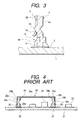
- solder-rise preventing means H are formed between the retaining portions 4c and the circuit board 1, the rise of the solder 5 is prevented by the solder-rise preventing means H upon melting of the creamy solder and the solder 5 does not reach the retaining portions 4c, as shown in Figs. 1 and 2. Consequently, the engagement between the engaging holes 6c and the retaining portions 4c is ensured and there is no fear of disengagement of the cover 6 nor is there any fear of the cover becoming unengageable.
- the solder-rise preventing means H are formed between the circuit board 1 and the retaining portions 4c, the rise of the solder 5 is prevented by the solder-rise preventing means H and the solder 5 does not reach the retaining portions 4c. Consequently, in comparison with the prior art, the engagement between the engaging holes 6c and the retaining portions 4c is ensured.
- solder-rise preventing means H are formed by the convex portions 4d on the frame 4, there can be provided a transmitter-receiver unit whose construction is simple and which is high in productivity and less expensive.
Landscapes
- Engineering & Computer Science (AREA)
- Microelectronics & Electronic Packaging (AREA)
- Manufacturing & Machinery (AREA)
- Shielding Devices Or Components To Electric Or Magnetic Fields (AREA)
- Casings For Electric Apparatus (AREA)
- Telephone Set Structure (AREA)
- Structure Of Receivers (AREA)
- Mounting Of Printed Circuit Boards And The Like (AREA)
- Fire Alarms (AREA)
Applications Claiming Priority (2)
| Application Number | Priority Date | Filing Date | Title |
|---|---|---|---|
| JP2000017951 | 2000-01-24 | ||
| JP2000017951A JP2001210971A (ja) | 2000-01-24 | 2000-01-24 | 送受信ユニット |
Publications (3)
| Publication Number | Publication Date |
|---|---|
| EP1121006A2 true EP1121006A2 (de) | 2001-08-01 |
| EP1121006A3 EP1121006A3 (de) | 2003-05-21 |
| EP1121006B1 EP1121006B1 (de) | 2007-10-03 |
Family
ID=18544867
Family Applications (1)
| Application Number | Title | Priority Date | Filing Date |
|---|---|---|---|
| EP00311220A Expired - Lifetime EP1121006B1 (de) | 2000-01-24 | 2000-12-15 | Sende-Empfangseinheit zur Sicherstellung der Montage einer Abdeckung auf einem Metallrahmen |
Country Status (6)
| Country | Link |
|---|---|
| US (1) | US20010009503A1 (de) |
| EP (1) | EP1121006B1 (de) |
| JP (1) | JP2001210971A (de) |
| KR (1) | KR100385103B1 (de) |
| CN (1) | CN1319977A (de) |
| DE (1) | DE60036600D1 (de) |
Families Citing this family (3)
| Publication number | Priority date | Publication date | Assignee | Title |
|---|---|---|---|---|
| JP5658491B2 (ja) | 2010-06-28 | 2015-01-28 | パナソニック株式会社 | 電子機器収納ケース |
| JP2013168508A (ja) * | 2012-02-15 | 2013-08-29 | Seiwa Electric Mfg Co Ltd | 表面実装クリップ |
| US20160135282A1 (en) * | 2014-11-07 | 2016-05-12 | Kabushiki Kaisha Toshiba | Electronic apparatus |
Family Cites Families (7)
| Publication number | Priority date | Publication date | Assignee | Title |
|---|---|---|---|---|
| DE3233620C2 (de) * | 1982-09-10 | 1984-07-26 | Standard Elektrik Lorenz Ag, 7000 Stuttgart | Leiterplattenanordnung mit einer Leiterplatte und einer daran mittels Lötstellen befestigter Metallwand |
| JPH01315167A (ja) * | 1988-03-01 | 1989-12-20 | Oki Electric Ind Co Ltd | 半導体装置 |
| JPH05283887A (ja) * | 1992-03-31 | 1993-10-29 | Toshiba Lighting & Technol Corp | 電磁シールドカバー及び電磁シールド部品 |
| JPH06104366A (ja) * | 1992-09-21 | 1994-04-15 | Kawasaki Steel Corp | 半導体パッケージおよびその実装方法 |
| JPH07147495A (ja) * | 1993-11-26 | 1995-06-06 | Nec Corp | プリント基板表面実装用シールドケース |
| JP3023282U (ja) * | 1995-09-14 | 1996-04-16 | モレックス インコーポレーテッド | 電気コネクタ |
| SE507255C2 (sv) * | 1996-08-22 | 1998-05-04 | Ericsson Telefon Ab L M | Skärmskydd |
-
2000
- 2000-01-24 JP JP2000017951A patent/JP2001210971A/ja not_active Withdrawn
- 2000-12-15 EP EP00311220A patent/EP1121006B1/de not_active Expired - Lifetime
- 2000-12-15 DE DE60036600T patent/DE60036600D1/de not_active Expired - Lifetime
-
2001
- 2001-01-10 US US09/758,569 patent/US20010009503A1/en not_active Abandoned
- 2001-01-16 CN CN01100578A patent/CN1319977A/zh active Pending
- 2001-01-19 KR KR10-2001-0003053A patent/KR100385103B1/ko not_active Expired - Fee Related
Also Published As
| Publication number | Publication date |
|---|---|
| CN1319977A (zh) | 2001-10-31 |
| US20010009503A1 (en) | 2001-07-26 |
| EP1121006B1 (de) | 2007-10-03 |
| DE60036600D1 (de) | 2007-11-15 |
| KR100385103B1 (ko) | 2003-05-23 |
| JP2001210971A (ja) | 2001-08-03 |
| KR20010076365A (ko) | 2001-08-11 |
| EP1121006A3 (de) | 2003-05-21 |
Similar Documents
| Publication | Publication Date | Title |
|---|---|---|
| JP3597368B2 (ja) | 電子機器 | |
| US20090016039A1 (en) | Structure And Method For Attaching Shield Case To Circuit Board, Electronic Component Module And Portable Telephone | |
| EP0702512B1 (de) | Abschirmungsvorrichtung und Verfahren zur Montage | |
| JP2005276626A (ja) | 電子部品取付用ソケット | |
| US5398166A (en) | Electronic component and mounting structure thereof | |
| EP1121006B1 (de) | Sende-Empfangseinheit zur Sicherstellung der Montage einer Abdeckung auf einem Metallrahmen | |
| JP4500726B2 (ja) | 高周波機器の取付構造 | |
| EP0957665B1 (de) | Elektronische Einrichtung | |
| US6950309B2 (en) | Power amplifier module assembly | |
| JP2009158586A (ja) | 高周波回路ユニット | |
| KR100272806B1 (ko) | 단자가부착된부품의설치구조 | |
| KR100714573B1 (ko) | 탄성형 방열부를 구비하는 튜너 | |
| JP2000077834A (ja) | 印刷配線板 | |
| KR200328309Y1 (ko) | 플라이백 트랜스 포머의 케이스 구조 | |
| JPH0526799Y2 (de) | ||
| JPH05335773A (ja) | シールドケース構体 | |
| EP1515598B1 (de) | Abschirmvorrichtung für eine Leiterplatte und deren Herstellungsverfahren | |
| JPH0642393Y2 (ja) | 高周波機器のシールドケース | |
| JPH11330765A (ja) | 表面実装モジュール | |
| JP3623637B2 (ja) | 電子機器 | |
| JPH0679197U (ja) | 電磁波シールドケースの取付構造 | |
| KR20060119940A (ko) | 회로 기판용 실드 및 실드의 제조 방법 | |
| KR20090011606A (ko) | 튜너 샤시 | |
| JP2005183545A (ja) | 受光モジュール | |
| JP2009099794A (ja) | 電子回路ユニット |
Legal Events
| Date | Code | Title | Description |
|---|---|---|---|
| PUAI | Public reference made under article 153(3) epc to a published international application that has entered the european phase |
Free format text: ORIGINAL CODE: 0009012 |
|
| AK | Designated contracting states |
Kind code of ref document: A2 Designated state(s): AT BE CH CY DE DK ES FI FR GB GR IE IT LI LU MC NL PT SE TR |
|
| AX | Request for extension of the european patent |
Free format text: AL;LT;LV;MK;RO;SI |
|
| PUAL | Search report despatched |
Free format text: ORIGINAL CODE: 0009013 |
|
| AK | Designated contracting states |
Designated state(s): AT BE CH CY DE DK ES FI FR GB GR IE IT LI LU MC NL PT SE TR |
|
| AX | Request for extension of the european patent |
Extension state: AL LT LV MK RO SI |
|
| 17P | Request for examination filed |
Effective date: 20030519 |
|
| AKX | Designation fees paid |
Designated state(s): DE FR GB |
|
| RTI1 | Title (correction) |
Free format text: TRANSMITTER-RECEIVER UNIT THAT ENSURES MOUNTING OF A COVER ON A METALLIC FRAME |
|
| GRAP | Despatch of communication of intention to grant a patent |
Free format text: ORIGINAL CODE: EPIDOSNIGR1 |
|
| GRAS | Grant fee paid |
Free format text: ORIGINAL CODE: EPIDOSNIGR3 |
|
| GRAA | (expected) grant |
Free format text: ORIGINAL CODE: 0009210 |
|
| AK | Designated contracting states |
Kind code of ref document: B1 Designated state(s): DE FR GB |
|
| REG | Reference to a national code |
Ref country code: GB Ref legal event code: FG4D |
|
| REF | Corresponds to: |
Ref document number: 60036600 Country of ref document: DE Date of ref document: 20071115 Kind code of ref document: P |
|
| EN | Fr: translation not filed | ||
| PG25 | Lapsed in a contracting state [announced via postgrant information from national office to epo] |
Ref country code: DE Free format text: LAPSE BECAUSE OF FAILURE TO SUBMIT A TRANSLATION OF THE DESCRIPTION OR TO PAY THE FEE WITHIN THE PRESCRIBED TIME-LIMIT Effective date: 20080107 |
|
| PLBE | No opposition filed within time limit |
Free format text: ORIGINAL CODE: 0009261 |
|
| STAA | Information on the status of an ep patent application or granted ep patent |
Free format text: STATUS: NO OPPOSITION FILED WITHIN TIME LIMIT |
|
| 26N | No opposition filed |
Effective date: 20080704 |
|
| GBPC | Gb: european patent ceased through non-payment of renewal fee |
Effective date: 20080103 |
|
| PG25 | Lapsed in a contracting state [announced via postgrant information from national office to epo] |
Ref country code: FR Free format text: LAPSE BECAUSE OF FAILURE TO SUBMIT A TRANSLATION OF THE DESCRIPTION OR TO PAY THE FEE WITHIN THE PRESCRIBED TIME-LIMIT Effective date: 20080704 |
|
| PG25 | Lapsed in a contracting state [announced via postgrant information from national office to epo] |
Ref country code: GB Free format text: LAPSE BECAUSE OF NON-PAYMENT OF DUE FEES Effective date: 20080103 |