EP1122776A2 - Verfahren zur Herstellung von Halbleiterchips - Google Patents
Verfahren zur Herstellung von Halbleiterchips Download PDFInfo
- Publication number
- EP1122776A2 EP1122776A2 EP01301093A EP01301093A EP1122776A2 EP 1122776 A2 EP1122776 A2 EP 1122776A2 EP 01301093 A EP01301093 A EP 01301093A EP 01301093 A EP01301093 A EP 01301093A EP 1122776 A2 EP1122776 A2 EP 1122776A2
- Authority
- EP
- European Patent Office
- Prior art keywords
- pressure sensitive
- sensitive adhesive
- semiconductor chips
- coated sheet
- double coated
- Prior art date
- Legal status (The legal status is an assumption and is not a legal conclusion. Google has not performed a legal analysis and makes no representation as to the accuracy of the status listed.)
- Granted
Links
Images

Classifications
-
- H—ELECTRICITY
- H10—SEMICONDUCTOR DEVICES; ELECTRIC SOLID-STATE DEVICES NOT OTHERWISE PROVIDED FOR
- H10P—GENERIC PROCESSES OR APPARATUS FOR THE MANUFACTURE OR TREATMENT OF DEVICES COVERED BY CLASS H10
- H10P72/00—Handling or holding of wafers, substrates or devices during manufacture or treatment thereof
- H10P72/70—Handling or holding of wafers, substrates or devices during manufacture or treatment thereof for supporting or gripping
- H10P72/74—Handling or holding of wafers, substrates or devices during manufacture or treatment thereof for supporting or gripping using temporarily an auxiliary support
- H10P72/7402—Wafer tapes, e.g. grinding or dicing support tapes
-
- H—ELECTRICITY
- H10—SEMICONDUCTOR DEVICES; ELECTRIC SOLID-STATE DEVICES NOT OTHERWISE PROVIDED FOR
- H10P—GENERIC PROCESSES OR APPARATUS FOR THE MANUFACTURE OR TREATMENT OF DEVICES COVERED BY CLASS H10
- H10P54/00—Cutting or separating of wafers, substrates or parts of devices
-
- H—ELECTRICITY
- H10—SEMICONDUCTOR DEVICES; ELECTRIC SOLID-STATE DEVICES NOT OTHERWISE PROVIDED FOR
- H10P—GENERIC PROCESSES OR APPARATUS FOR THE MANUFACTURE OR TREATMENT OF DEVICES COVERED BY CLASS H10
- H10P72/00—Handling or holding of wafers, substrates or devices during manufacture or treatment thereof
- H10P72/70—Handling or holding of wafers, substrates or devices during manufacture or treatment thereof for supporting or gripping
- H10P72/74—Handling or holding of wafers, substrates or devices during manufacture or treatment thereof for supporting or gripping using temporarily an auxiliary support
- H10P72/7402—Wafer tapes, e.g. grinding or dicing support tapes
- H10P72/7404—Wafer tapes, e.g. grinding or dicing support tapes the wafer tape being a laminate of three or more layers, e.g. including additional layers beyond a base layer and an uppermost adhesive layer
-
- H—ELECTRICITY
- H10—SEMICONDUCTOR DEVICES; ELECTRIC SOLID-STATE DEVICES NOT OTHERWISE PROVIDED FOR
- H10P—GENERIC PROCESSES OR APPARATUS FOR THE MANUFACTURE OR TREATMENT OF DEVICES COVERED BY CLASS H10
- H10P72/00—Handling or holding of wafers, substrates or devices during manufacture or treatment thereof
- H10P72/70—Handling or holding of wafers, substrates or devices during manufacture or treatment thereof for supporting or gripping
- H10P72/74—Handling or holding of wafers, substrates or devices during manufacture or treatment thereof for supporting or gripping using temporarily an auxiliary support
- H10P72/7416—Handling or holding of wafers, substrates or devices during manufacture or treatment thereof for supporting or gripping using temporarily an auxiliary support used during dicing or grinding
Definitions
- the present invention relates to a process for producing semiconductor chips. More particularly, the present invention relates to a process for producing semiconductor chips with high yield without suffering from damaging of semiconductor chips.
- the applicant in Japanese Patent Application No. 11(1999)-109806, has proposed a technique utilizing a pressure sensitive adhesive double coated sheet including a heat shrink base.
- a semiconductor wafer is fixed on a hard plate by means of the pressure sensitive adhesive double coated sheet, and subsequently required processing is performed to thereby form the semiconductor wafer into semiconductor chips.
- the pressure sensitive adhesive double coated sheet is heated to thereby effect a heat shrink of the base of the double coated sheet with the result that the pressure sensitive adhesive layer of the double coated sheet is deformed.
- the deformation of the pressure sensitive adhesive layer reduces the area of contact of the semiconductor chips with the pressure sensitive adhesive layer to thereby result in reduction of adherence. This facilitates the pickup of the semiconductor chips.
- it is requisite to dice the semiconductor wafer from back thereof. In the event of chip cracking, it is likely to occur at the circuit surface thereof to thereby invite the danger of lowering the yield of semiconductor chips.
- the present invention has been made in view of the above state of the prior art.
- the process for producing semiconductor chips according to the present invention comprises the steps of:
- both the pressure sensitive adhesive layers of the pressure sensitive adhesive double coated sheet be composed of an energy radiation curable pressure sensitive adhesive. Further, in the present invention, it is preferred that, after the stripping of the dicing tape from the semiconductor chips but before the irradiating of the pressure sensitive adhesive double coated sheet, from the transparent hard plate side, with energy radiation, backs of the semiconductor chips exposed by the stripping of the dicing tape are ground.
- the above present invention enables producing semiconductor chips of extremely reduced thickness in high production efficiency while minimizing the damaging thereof.
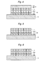
- Figures 1 to 6 show the steps to be performed in the process for picking up semiconductor chips.
- semiconductor wafer 1 having a surface overlaid with circuits is provided, and a back of the semiconductor wafer is fixed on dicing tape 2.
- Pressure sensitive adhesive double coated sheet 10 is stuck to a circuit surface of the semiconductor wafer in order to protect the circuit surface.
- Formation of circuits on a surface of a semiconductor wafer is accomplished by customary means such as the etching or the lift-off technique. After the circuit formation, the back of the semiconductor wafer may be ground so as to regulate the thickness thereof to desirable one.
- a dicing tape comprising base 2a and, overlaid thereon, pressure sensitive adhesive layer 2b which is curable upon exposure to energy radiation (energy rays or energy beams) is preferably used in the present invention.
- the periphery of the dicing tape 2 is secured to circular or rectangular ring frame 3.
- the pressure sensitive adhesive double coated sheet 10 for use in the present invention comprises shrink base 11 having its both sides overlaid with pressure sensitive adhesive layers 12a, 12b. At least one of the pressure sensitive adhesive layers 12a, 12b is composed of an energy radiation curable pressure sensitive adhesive.
- the energy radiation curable pressure sensitive adhesive is preferably used in the side of pressure sensitive adhesive layer 12a to which the semiconductor wafer 1 is stuck.
- the energy radiation curable pressure sensitive adhesive layer has the property of curing upon being exposed to energy radiation with the result that the adherence to semiconductor chips is reduced.
- Upper surface of the pressure sensitive adhesive layer 12b not stuck to the semiconductor wafer 1 may be overlaid with release liner 13 for protecting the pressure sensitive adhesive layer.
- Fig. 1 The arrangement of Fig. 1 can be realized through various courses including various pretreatments to be performed in the processing of semiconductors. Therefore, what courses have been taken for the realization of the above arrangement are not particularly limited in the present invention.
- the arrangement of Fig. 1 is realized by first sticking the dicing tape 2 to the back of one semiconductor wafer 1 and securing the periphery of the dicing tape 2 to the ring frame 3 and thereafter sticking the pressure sensitive adhesive double coated sheet 10 to the circuit surface of the semiconductor wafer 1.
- the arrangement of Fig. 1 may be realized by first sticking the pressure sensitive adhesive double coated sheet 10 to the circuit surface of the semiconductor wafer 1 and thereafter fixing the back of one semiconductor wafer 1 on the dicing tape 2 and securing the periphery of the dicing tape 2 to the ring frame 3.
- the semiconductor wafer 1 in the state of having the pressure sensitive adhesive double coated sheet 10 stuck thereto is diced circuit by circuit to thereby form semiconductor chips 4.
- all the base 11, pressure sensitive adhesive layers 12a, 12b and release liner 13 which constitute the pressure sensitive adhesive double coated sheet 10 are transparent.
- Various dicing devices having commonly been employed in the art can be used in this dicing without any particular limitation.
- the semiconductor chips 4 are fixed on transparent hard plate 5 by adherence of the pressure sensitive adhesive layer 12b of the pressure sensitive adhesive double coated sheet 10.
- the release liner 13 is stuck onto the pressure sensitive adhesive layer 12b, the release liner 13 is removed in advance to thereby expose the pressure sensitive adhesive layer 12b and thereafter the semiconductor chips 4 are fixed on the transparent hard plate 5 by means of the pressure sensitive adhesive layer 12b.
- the release liner 13 can be stripped from the pressure sensitive adhesive layer 12b by, for example, the method in which, referring to Fig. 3, pressure sensitive adhesive sheet 6 with a diameter larger than that of the semiconductor wafer 1 is stuck to the entire surface of the release liner 13 and thereafter a peeling strength is applied to the pressure sensitive adhesive sheet 6.
- the fixing of the semiconductor chips 4 on the transparent hard plate 5 is performed while the semiconductor chips 4 are stuck to the dicing tape 2. Therefore, the alignment of the semiconductor chips is maintained.
- the periphery of the dicing tape 2 is preferably cut so that the diameter of the dicing tape 2 conforms to that of the semiconductor wafer. This removes excess portion of the dicing tape 2 to thereby enable enhancing operation efficiency.
- the dicing tape 2 is stripped from the backs of the semiconductor chips 4.
- the stripping of the dicing tape 2 is appropriately performed in conformity with the properties of employed tape.
- a pressure sensitive adhesive sheet may be stuck to the entire surface of the dicing tape 2, followed by peeling the pressure sensitive adhesive sheet from the dicing tape.
- the dicing tape 2 comprises energy radiation curable pressure sensitive adhesive layer 2b
- the stripping off of the dicing tape 2 can be facilitated by irradiating the dicing tape 2 from its base 2a side with energy radiation to thereby reduce the adhesive strength of the energy radiation curable pressure sensitive adhesive layer 2b.
- the backs of the semiconductor chips 4 are exposed as shown in Fig. 5.
- the semiconductor chips 4 may further be processed according to necessity.
- the backs of the individual semiconductor chips 4 may be ground so as to reduce the thickness of the semiconductor chips 4.
- the pressure sensitive adhesive double coated sheet 10 is exposed to energy radiation.
- the exposing to energy radiation may be performed over the entire surface of the pressure sensitive adhesive double coated sheet 10 or on a spot basis on portions where semiconductor chips to be picked up are secured.
- the energy radiation passes through the transparent hard plate 5, the pressure sensitive adhesive layer 12b and the base 11 and reaches the energy radiation curable pressure sensitive adhesive layer 12a. Accordingly, when ultraviolet radiation is used as the energy radiation, transparent pressure sensitive adhesive layer 12b and transparent base 11 are employed.
- the energy radiation curable pressure sensitive adhesive layer 12a is cured by the exposure to energy radiation, so that the adherence thereof is reduced or vanished to thereby enable stripping of the semiconductor chips 4.
- the exposure to energy radiation is performed by common means such as an ultraviolet lamp or a high pressure mercury lamp.
- a condensing (converging) lens, a reflecting mirror or the like can be employed.
- the pressure sensitive adhesive double coated sheet 10 is heated after or simultaneously with the exposure to energy radiation.
- the heating is performed by, for example, a hot plate or a heater.
- the heating may also be performed on a spot basis with the use of heat rays.
- the exposure to heat rays is performed on a spot basis on portions where semiconductor chips to be picked up are secured and where they have been or are exposed to energy radiatior
- the exposure to heat rays is performed by a halogen lamp, a xenon lamp or a high pressure mercury lamp.
- a condensing (converging) lens or a reflecting mirror can be employed.
- the exposure to heat rays may be performed from the side of transparent hard plate 5 or the side of semiconductor chips 4.
- the heating be carried out so that the temperature of the pressure sensitive adhesive double-coated sheet 10 is raised to especially about 100-300°C, still especially about 150 - 200°C.
- the high pressure mercury lamp can simultaneously function as an energy radiation source and as a heat ray source. Accordingly, the spot exposure to energy radiation and heat rays can be simultaneously accomplished by the use of the high pressure mercury lamp. In the use of the high pressure mercury lamp, the exposure is performed from the side of transparent hard plate 5.
- the above heating causes the pressure sensitive adhesive double coated sheet 10 to deform to thereby reduce the area of contact of the semiconductor chips 4 with the pressure sensitive adhesive layer 12a of the pressure sensitive adhesive double coated sheet 10.
- the pickup of the semiconductor chips 4 is facilitated.
- the use of the shrinkable base 11 promotes the deformation of the pressure sensitive adhesive double coated sheet 10.
- the heating causes the pressure sensitive adhesive double coated sheet 10 to deform to thereby reduce the area of contact of the semiconductor chips 4 with the pressure sensitive adhesive layer 12a. Furthermore, the adhesive force of the pressure sensitive adhesive layer 12a is lowered by exposure to energy radiation. As a result, the semiconductor chips 4 can be easily picked up by common means such as a suction collet. Thus, selective pickup of semiconductor chips can be effected, and operation efficiency can be enhanced.
- the pressure sensitive adhesive double coated sheet 10 for use in the present invention will now be described.
- the pressure sensitive adhesive double coated sheet 10 comprises shrinkable base 11 having its both sides overlaid with pressure sensitive adhesive layers 12a, 12b.
- the base 11 although not particularly limited as long as it is shrinkable, can be selected from among, for example, films of polyethylene, polypropylene, polybutene, polybutadiene, polymethylpentene, polyvinyl chloride, vinyl chloride copolymers, polyethylene terephthalate, polybutylene terephthalate, polyurethanes, ethylene/vinyl acetate copolymer, ionomer resins, ethylene/(meth)acrylic acid copolymer, ethylene/(meth)acrylic ester copolymers, polystyrene polycarbonate and fluororesin, films produced by crosslinking these and films composed of laminates thereof. Furthermore, according to necessity, use can be made of films produced by coloring the above films. These films may be produced by extrusion or casting.
- the thickness of the base is generally in the range of 5 to 300 ⁇ m, preferably 10 to 200 ⁇ m.
- heat shrinkable films are preferably employed as the base in the present invention.
- the shrinkage factor (shrinkage ratio) of the shrinkable film preferably employed in the present invention is preferably in the range of 10 to 90%, still preferably 20 to 80%.
- the above shrinkage factor values are those calculated from the dimensions of film measured before and after heating at 120°C.
- uniaxially or biaxially oriented films of polyethylene, polypropylene, polyethylene terephthalate or the like be used as the heat shrinkable film.
- the shrinkable film may be a laminate of films whose shrinkage factors are different from each other.
- the laminate composed of films whose shrinkage factors are different from each other is used as the base 11, a protrudent deformation is likely to occur on the lower shrinkage factor side, so that the sticking of the semiconductor chips 4 is only made by point contacts to thereby extremely facilitate the removement of the semiconductor chips 4.
- the energy radiation curable pressure sensitive adhesive layer is irradiated with energy radiation after the completion of requisite steps.
- energy radiation when ultraviolet radiation is used as the energy radiation, all the films constituting the shrinkable base 11 must be permeable for ultraviolet ray.
- the pressure sensitive adhesive double coated sheet 10 comprises the shrinkable base 11 having its both sides overlaid with pressure sensitive adhesive layers 12a, 12b, at least one (one or both) of the pressure sensitive adhesive layers composed of an energy radiation curable pressure sensitive adhesive. It is preferred that the pressure sensitive adhesive layer 12a stuck to the semiconductor wafer 1 (or semiconductor chips 4) is composed of an energy radiation curable pressure sensitive adhesive. Although it is also preferred that the other pressure sensitive adhesive layer 12b stuck to the transparent hard plate 5 is composed of an energy radiation curable pressure sensitive adhesive, this is not inevitably requisite as long as the pressure sensitive adhesive layer 12a is composed of an energy radiation curable pressure sensitive adhesive.
- both the pressure sensitive adhesive layers 12a, 12b are composed of energy radiation curable pressure sensitive adhesives
- these energy radiation curable pressure sensitive adhesives are preferably selected so that the elastic modulus of pressure sensitive adhesive layer 12a having been cured (elastic modulus 12a) is higher than the elastic modulus of pressure sensitive adhesive layer 12b having been cured (elastic modulus 12b).
- the elastic modulus 12a is preferably at least two times the elastic modulus 12b, still preferably at least five times the elastic modulus 12b.
- the energy radiation curable pressure sensitive adhesive generally comprises an acrylic pressure sensitive adhesive and an energy radiation polymerizable compound as main components.
- the acrylic pressure sensitive adhesive for use in the present invention comprises a copolymer of a monomer consisting mainly of an acrylic acid alkyl ester or a methacrylic acid alkyl ester, and increases the adherence and cohesive strength of energy radiation curable pressure sensitive adhesive before curing.
- low-molecular-weight compounds having in the molecule thereof at least two photopolymerizable carbon to carbon double bonds that can be converted into a three-dimensional network structure by light irradiation as disclosed in Japanese Patent Laid-open Publication Nos. 60(1985)-196,956 and 60(1985)-223,139 are widely used as the energy radiation polymerizable compounds to be incorporated in the energy radiation curable pressure sensitive adhesives.
- Specific examples thereof include trimethylolpropane triacrylate, pentaerythritol triacrylate, pentaerythritol tetraacrylate, dipentaery-thritol monohydroxypentaacrylate, dipentaerythritol hexaacrylate, 1,4-butylene glycol diacrylate, 1,6-hexanediol diacrylate, polyethylene glycol diacrylate and commercially available oligoester acrylates.
- Urethane acrylate oligomers can be used as the energy radiation polymerizable compounds.
- Urethane acrylate oligomers can be obtained by first reacting a polyester or polyether polyol compound with a polyisocyanate compound such as 2,4-tolylene diisocyanate, 2,6-tolylene diisocyanate, 1,3-xylylene diisocyanate, 1,4-xylylene diisocyanate or diphenylmethane-4,4-diisocyanate to thereby obtain an isocyanate terminated urethane prepolymer and by thereafter reacting the obtained isocyanate terminated urethane prepolymer with a hydroxyl group containing acrylate or methacrylate, for example, 2-hydroxyethyl acrylate, 2-hydroxyethyl methacrylate, 2-hydroxypropyl acrylate, 2-hydroxypropyl methacrylate, polyethylene glycol acrylate or polyethylene glycol methacrylate,
- the blending ratio of energy radiation polymerizable compound to acrylic pressure sensitive adhesive in the energy radiation curable pressure sensitive adhesive it is preferred that 50 to 200 parts by weight of the energy radiation polymerizable compound is used per 100 parts by weight of the acrylic pressure sensitive adhesive.
- the initial adhesive strength of the obtained pressure sensitive adhesive sheet is large, and the adhesive strength is sharply dropped upon irradiation of the pressure sensitive adhesive layer with energy radiation. Accordingly, the peeling at the interface of the semiconductor chips 4 and the acrylic energy radiation curable pressure sensitive adhesive layer 12a is facilitated to thereby enable picking up of the semiconductor chips 4.
- the energy radiation curable pressure sensitive adhesive layer may be composed of an energy radiation curable copolymer having an energy radiation polymerizable group as a side chain. This energy radiation curable copolymer simultaneously exhibits satisfactory adherence and energy radiation curability properties. Details of the energy radiation curable copolymer having an energy radiation polymerizable group as a side chain are described in, for example, Japanese Patent Laid-open Publication Nos. 5(1993)-32946 and 8(1996)-27239.
- the above acrylic energy radiation curable pressure sensitive adhesive possesses satisfactory adhesive strength to the semiconductor chips 4 before exposure to energy radiation, and the adhesive strength is extremely decreased upon exposure to energy radiation. That is, the acrylic energy radiation curable pressure sensitive adhesive enables securing the semiconductor chips 4 with satisfactory adhesive strength before exposure to energy radiation, but, after exposure to energy radiation, enables easily detaching the semiconductor chips 4 therefrom.
- the other pressure sensitive adhesive layer 12b can be formed from various conventional pressure sensitive adhesives. These pressure sensitive adhesives are not limited at all. As examples thereof, there can be mentioned peelable pressure sensitive adhesives based on rubbers, acrylics, silicones, polyurethanes and polyvinyl ethers. However, in the present invention, it is preferred that the pressure sensitive adhesive layer 12b also be composed of the above energy radiation curable pressure sensitive adhesive.
- each of the pressure sensitive adhesive layers 12a, 12b is generally in the range of about 3 to 100 ⁇ m, preferably about 10 to 50 ⁇ m.
- Transparent resin films for example, a film of a polyolefin such as polyethylene or polypropylene and a polyethylene terephthalate film are used as the optionally employed release liner 13.
- the transparent hard plate 5 there can be employed, for example, a glass plate, a quartz plate or a plastic plate such as a plate of acrylic, polyvinyl chloride, polyethylene terephthalate, polypropylene or polycarbonate.
- the hardness, defined by ASTM D 883, of the transparent hard plate 5 is preferably at least 70 MPa.
- the thickness of the transparent hard plate 5, although depending on the properties of the material used therein, is generally in the range of about 0.1 to 10mm. Those which are permeable for energy radiation and heat rays for use in the present invention are used as the transparent hard plate 5.
- the present invention provides at least in preferred embodiments the process for producing semiconductor chips with high yield while minimizing the damaging of semiconductor chips, even if the thickness thereof is extremely reduced, and while avoiding the chip cracking on the circuit side of the semiconductor chips.
- an acrylic pressure sensitive adhesive copolymer of 91 parts by weight of n-butyl acrylate and 9 parts by weight of acrylic acid
- 120 parts by weight of urethane acrylate oligomer weight average molecular weight: about 10,000, produced by Dainichiseika Color And Chemicals Manufacturing Company Limited
- 2 parts by weight of isocyanate crosslinking agent trade name: Coronate L, produced by Nippon Polyurethane Co., Ltd.
- initiator for energy radiation curing reaction ⁇ -hydroxycyclohexyl phenyl ketone
- a 38 ⁇ m thick polyethylene terephthalate film having undergone a release treatment using a silicone release agent was coated with a pressure sensitive adhesive composition (the elastic modulus thereof after ultraviolet irradiation was 9.0 x 10 8 Pa), produced in the same manner as in the step 1(1) except that 50 parts by weight of urethane acrylate oligomer (weight average molecular weight: about 1000) was employed, so that the thickness of the coating was 15 ⁇ m and heated at 100°C for 1 min.
- urethane acrylate oligomer weight average molecular weight: about 1000
- Dicing tape (Adwill D-218, manufactured by Lintec Corporation) was stuck to an unpolished surface of a silicon wafer of 6 inch diameter and 750 ⁇ m thickness.
- the above produced pressure sensitive adhesive double coated sheet (pressure sensitive adhesive layer of step 1-(3)) was stuck to a specular surface of the silicon wafer.
- the polyethylene terephthalate film (38 ⁇ m) as a release liner remained stuck to the pressure sensitive adhesive layer of pressure sensitive adhesive double coated sheet which was not stuck to the silicon wafer.
- the wafer together with the pressure sensitive adhesive double coated sheet was diced into 10 mm squares by the use of dicing device (AWD-4000B, manufactured by Tokyo Seimitsu Co., Ltd.).
- the polyethylene terephthalate film was stripped off with the use of pressure sensitive adhesive sheet for stripping (Adwill S-6, manufactured by Lintec Corporation).
- the thus exposed pressure sensitive adhesive layer pressure sensitive adhesive layer of step 1-(1) above was stuck to a transparent hard plate (700 ⁇ m thick glass).
- the dicing tape was cut so that the diameter of the dicing tape conformed with that of the wafer.
- the dicing tape on its base side was irradiated with ultraviolet rays by the use of ultraviolet irradiator (RAD-2000/m8, manufactured by Lintec Corporation), and the dicing tape was stripped off.
- the thus exposed unpolished surfaces of semiconductor chips were ground by means of back grinder (DFG-840, manufactured by Disco Corporation) so that the thickness of the semiconductor chips became 30 ⁇ m.
- the glass side was exposed to ultraviolet rays, and the whole was allowed to stand still on a hot plate of 160°C for 5 min.
- the semiconductor chips were detached from the pressure sensitive adhesive double coated sheet. The detachment was easily accomplished without chip damaging.
- Example 2 The same procedure as in Example 1 was repeated except that, without the use of the hot plate, spot exposure (output: 300 W, distance: 10 cm, and exposure time: 5 sec) was performed chip by chip by employing a xenon lamp and by condensing heat rays into a 5 mm diameter. The semiconductor chips at portions having been exposed to heat rays were detached. The detachment was easily accomplished without chip damaging.
Landscapes
- Dicing (AREA)
- Mechanical Treatment Of Semiconductor (AREA)
- Container, Conveyance, Adherence, Positioning, Of Wafer (AREA)
Applications Claiming Priority (2)
| Application Number | Priority Date | Filing Date | Title |
|---|---|---|---|
| JP2000028702 | 2000-02-07 | ||
| JP2000028702A JP4392732B2 (ja) | 2000-02-07 | 2000-02-07 | 半導体チップの製造方法 |
Publications (4)
| Publication Number | Publication Date |
|---|---|
| EP1122776A2 true EP1122776A2 (de) | 2001-08-08 |
| EP1122776A3 EP1122776A3 (de) | 2004-01-28 |
| EP1122776B1 EP1122776B1 (de) | 2007-04-04 |
| EP1122776B8 EP1122776B8 (de) | 2007-06-06 |
Family
ID=18554067
Family Applications (1)
| Application Number | Title | Priority Date | Filing Date |
|---|---|---|---|
| EP01301093A Expired - Lifetime EP1122776B8 (de) | 2000-02-07 | 2001-02-07 | Verfahren zur Herstellung von Halbleiterchips |
Country Status (9)
| Country | Link |
|---|---|
| US (1) | US6436795B2 (de) |
| EP (1) | EP1122776B8 (de) |
| JP (1) | JP4392732B2 (de) |
| KR (1) | KR100661207B1 (de) |
| DE (1) | DE60127602T2 (de) |
| MY (1) | MY117437A (de) |
| PT (1) | PT1122776E (de) |
| SG (1) | SG90232A1 (de) |
| TW (1) | TW483115B (de) |
Cited By (6)
| Publication number | Priority date | Publication date | Assignee | Title |
|---|---|---|---|---|
| EP1542274A4 (de) * | 2002-08-28 | 2006-10-11 | Lintec Corp | Schutzstruktur eines halbleiterwafers, verfahren zum schutz eines halbleiterwafers, dabei verwendetes mehrschichtiges schutzblatt und verfahren zur herstellung eines halbleiterwafers |
| EP1484791A4 (de) * | 2002-03-04 | 2008-03-19 | Tokyo Electron Ltd | Zerschneideverfahren, verfahren zur untersuchung eines integrierten schaltungselements, substrathalteeinrichtung und druckhaftfilm |
| EP1865545A4 (de) * | 2005-03-29 | 2008-03-26 | Furukawa Electric Co Ltd | Klebeband zur zerteilung von wafern und chip-herstellungsverfahren damit |
| WO2008131287A1 (en) * | 2007-04-19 | 2008-10-30 | Micron Technology, Inc. | Semiconductor workpiece carriers and methods for processing semiconductor workpieces |
| EP2877547A4 (de) * | 2012-07-26 | 2016-01-27 | 3M Innovative Properties Co | Wärmelösliche haftartikel |
| US9637264B2 (en) | 2010-01-28 | 2017-05-02 | Avery Dennison Corporation | Label applicator belt system |
Families Citing this family (23)
| Publication number | Priority date | Publication date | Assignee | Title |
|---|---|---|---|---|
| JP2003218063A (ja) * | 2002-01-24 | 2003-07-31 | Canon Inc | ウエハ貼着用粘着シート及び該シートを利用する加工方法 |
| KR100735719B1 (ko) * | 2002-03-28 | 2007-07-06 | 미쓰이 가가쿠 가부시키가이샤 | 반도체웨이퍼 표면보호용 점착필름 및 상기 점착필름을사용하는 반도체웨이퍼의 보호방법 |
| JP4107417B2 (ja) * | 2002-10-15 | 2008-06-25 | 日東電工株式会社 | チップ状ワークの固定方法 |
| JP2005064239A (ja) * | 2003-08-12 | 2005-03-10 | Lintec Corp | 半導体装置の製造方法 |
| WO2005112091A1 (ja) * | 2004-05-18 | 2005-11-24 | Hitachi Chemical Co., Ltd. | 粘接着シート並びにそれを用いた半導体装置及びその製造方法 |
| KR100539271B1 (ko) * | 2004-07-26 | 2005-12-27 | 삼성전자주식회사 | 휨 방지 재질을 사용하는 반도체 칩의 다이 접착 방법 |
| US7238258B2 (en) * | 2005-04-22 | 2007-07-03 | Stats Chippac Ltd. | System for peeling semiconductor chips from tape |
| KR100716304B1 (ko) * | 2005-06-30 | 2007-05-08 | 엘지.필립스 엘시디 주식회사 | 액정 표시 장치용 인쇄판 및 그의 제조 방법 |
| WO2007057954A1 (ja) * | 2005-11-17 | 2007-05-24 | Fujitsu Limited | 半導体装置及びその製造方法 |
| KR100873286B1 (ko) * | 2006-12-29 | 2008-12-11 | 주식회사 실트론 | 실리콘 잉곳의 마운팅 장치 및 그 방법 |
| JP5135824B2 (ja) * | 2007-02-21 | 2013-02-06 | パナソニック株式会社 | 慣性力センサ素子の製造方法 |
| US8282754B2 (en) | 2007-04-05 | 2012-10-09 | Avery Dennison Corporation | Pressure sensitive shrink label |
| WO2008124581A1 (en) | 2007-04-05 | 2008-10-16 | Avery Dennison Corporation | Pressure sensitive shrink label |
| CN102460655B (zh) * | 2009-06-15 | 2015-05-13 | Lg化学株式会社 | 晶片处理薄片 |
| JP2011204806A (ja) * | 2010-03-24 | 2011-10-13 | Nitto Denko Corp | ウエハの加工方法 |
| JP2012104778A (ja) * | 2010-11-15 | 2012-05-31 | Disco Abrasive Syst Ltd | 光デバイスウエーハの分割方法 |
| JP5013148B1 (ja) * | 2011-02-16 | 2012-08-29 | 株式会社東京精密 | ワーク分割装置及びワーク分割方法 |
| JP5982248B2 (ja) * | 2012-09-28 | 2016-08-31 | 富士フイルム株式会社 | 半導体装置製造用仮接合層、積層体、及び、半導体装置の製造方法。 |
| JP5589045B2 (ja) * | 2012-10-23 | 2014-09-10 | 日東電工株式会社 | 半導体ウエハのマウント方法および半導体ウエハのマウント装置 |
| JP6704322B2 (ja) | 2015-09-30 | 2020-06-03 | 日東電工株式会社 | シートおよび複合シート |
| JP2017066485A (ja) * | 2015-09-30 | 2017-04-06 | 日東電工株式会社 | シートおよび複合シート |
| JP7041341B2 (ja) * | 2017-09-29 | 2022-03-24 | 日亜化学工業株式会社 | 発光素子の製造方法 |
| JP7110541B2 (ja) * | 2018-01-11 | 2022-08-02 | 株式会社東京精密 | ワーク分割装置及びワーク分割方法 |
Family Cites Families (14)
| Publication number | Priority date | Publication date | Assignee | Title |
|---|---|---|---|---|
| US5714029A (en) | 1984-03-12 | 1998-02-03 | Nitto Electric Industrial Co., Ltd. | Process for working a semiconductor wafer |
| JPH0616524B2 (ja) | 1984-03-12 | 1994-03-02 | 日東電工株式会社 | 半導体ウエハ固定用接着薄板 |
| JPS60223139A (ja) | 1984-04-18 | 1985-11-07 | Nitto Electric Ind Co Ltd | 半導体ウエハ固定用接着薄板 |
| JP2601956B2 (ja) | 1991-07-31 | 1997-04-23 | リンテック株式会社 | 再剥離型粘着性ポリマー |
| DE4230784A1 (de) * | 1992-09-15 | 1994-03-17 | Beiersdorf Ag | Durch Strahlung partiell entklebendes Selbstklebeband (Dicing Tape) |
| JP2984549B2 (ja) | 1994-07-12 | 1999-11-29 | リンテック株式会社 | エネルギー線硬化型感圧粘着剤組成物およびその利用方法 |
| JP3521099B2 (ja) * | 1994-11-29 | 2004-04-19 | リンテック株式会社 | ダイシング用リングフレームへの接着剤の付着防止用粘着シートおよび該粘着シートを備えたウェハ加工用シート |
| JP3438369B2 (ja) * | 1995-01-17 | 2003-08-18 | ソニー株式会社 | 部材の製造方法 |
| JP3496347B2 (ja) * | 1995-07-13 | 2004-02-09 | 株式会社デンソー | 半導体装置及びその製造方法 |
| US6007920A (en) * | 1996-01-22 | 1999-12-28 | Texas Instruments Japan, Ltd. | Wafer dicing/bonding sheet and process for producing semiconductor device |
| JP3955659B2 (ja) * | 1997-06-12 | 2007-08-08 | リンテック株式会社 | 電子部品のダイボンディング方法およびそれに使用されるダイボンディング装置 |
| JPH11109806A (ja) | 1997-10-06 | 1999-04-23 | Canon Inc | 画像形成装置 |
| US6140151A (en) * | 1998-05-22 | 2000-10-31 | Micron Technology, Inc. | Semiconductor wafer processing method |
| JP3784202B2 (ja) | 1998-08-26 | 2006-06-07 | リンテック株式会社 | 両面粘着シートおよびその使用方法 |
-
2000
- 2000-02-07 JP JP2000028702A patent/JP4392732B2/ja not_active Expired - Lifetime
-
2001
- 2001-02-05 TW TW090102392A patent/TW483115B/zh not_active IP Right Cessation
- 2001-02-06 SG SG200100650A patent/SG90232A1/en unknown
- 2001-02-06 KR KR1020010005522A patent/KR100661207B1/ko not_active Expired - Lifetime
- 2001-02-06 US US09/777,599 patent/US6436795B2/en not_active Expired - Lifetime
- 2001-02-06 MY MYPI20010517A patent/MY117437A/en unknown
- 2001-02-07 PT PT01301093T patent/PT1122776E/pt unknown
- 2001-02-07 DE DE60127602T patent/DE60127602T2/de not_active Expired - Fee Related
- 2001-02-07 EP EP01301093A patent/EP1122776B8/de not_active Expired - Lifetime
Cited By (13)
| Publication number | Priority date | Publication date | Assignee | Title |
|---|---|---|---|---|
| US8101436B2 (en) | 2002-03-04 | 2012-01-24 | Tokyo Electron Limited | Dicing method, method of inspecting integrated circuit element, substrate holding device, and pressure sensitive adhesive film |
| EP1484791A4 (de) * | 2002-03-04 | 2008-03-19 | Tokyo Electron Ltd | Zerschneideverfahren, verfahren zur untersuchung eines integrierten schaltungselements, substrathalteeinrichtung und druckhaftfilm |
| US7361971B2 (en) | 2002-08-28 | 2008-04-22 | Lintec Corporation | Semiconductor wafer protection structure and laminated protective sheet for use therein |
| EP2270848A3 (de) * | 2002-08-28 | 2012-04-18 | Lintec Corporation | Halbleiterwafer-Schutzstruktur und -verfahren, laminierte Schutzfolie zur Verwendung darin und Verfahren zur Halbleiterwaferverarbeitung |
| EP1542274A4 (de) * | 2002-08-28 | 2006-10-11 | Lintec Corp | Schutzstruktur eines halbleiterwafers, verfahren zum schutz eines halbleiterwafers, dabei verwendetes mehrschichtiges schutzblatt und verfahren zur herstellung eines halbleiterwafers |
| EP1865545A4 (de) * | 2005-03-29 | 2008-03-26 | Furukawa Electric Co Ltd | Klebeband zur zerteilung von wafern und chip-herstellungsverfahren damit |
| US7985474B2 (en) | 2005-03-29 | 2011-07-26 | The Furukawa Electric Co., Ltd. | Wafer-dicing adhesive tape and method of producing chips using the same |
| US8011513B2 (en) | 2007-04-19 | 2011-09-06 | Micron Technology, Inc. | Semiconductor workpiece carriers and methods for processing semiconductor workpieces |
| WO2008131287A1 (en) * | 2007-04-19 | 2008-10-30 | Micron Technology, Inc. | Semiconductor workpiece carriers and methods for processing semiconductor workpieces |
| TWI382453B (zh) * | 2007-04-19 | 2013-01-11 | 美光科技公司 | 半導體工件載體以及處理半導體工件之方法 |
| US8476109B2 (en) | 2007-04-19 | 2013-07-02 | Micron Technology, Inc. | Semiconductor workpiece carriers and methods for processing semiconductor workpieces |
| US9637264B2 (en) | 2010-01-28 | 2017-05-02 | Avery Dennison Corporation | Label applicator belt system |
| EP2877547A4 (de) * | 2012-07-26 | 2016-01-27 | 3M Innovative Properties Co | Wärmelösliche haftartikel |
Also Published As
| Publication number | Publication date |
|---|---|
| EP1122776B8 (de) | 2007-06-06 |
| TW483115B (en) | 2002-04-11 |
| PT1122776E (pt) | 2007-04-30 |
| US6436795B2 (en) | 2002-08-20 |
| EP1122776B1 (de) | 2007-04-04 |
| EP1122776A3 (de) | 2004-01-28 |
| DE60127602D1 (de) | 2007-05-16 |
| MY117437A (en) | 2004-06-30 |
| DE60127602T2 (de) | 2007-12-20 |
| SG90232A1 (en) | 2002-07-23 |
| KR100661207B1 (ko) | 2006-12-22 |
| US20010014492A1 (en) | 2001-08-16 |
| KR20010105152A (ko) | 2001-11-28 |
| JP4392732B2 (ja) | 2010-01-06 |
| JP2001217212A (ja) | 2001-08-10 |
Similar Documents
| Publication | Publication Date | Title |
|---|---|---|
| EP1122776B1 (de) | Verfahren zur Herstellung von Halbleiterchips | |
| US6398892B1 (en) | Method of using pressure sensitive adhesive double coated sheet | |
| JP4312419B2 (ja) | 半導体ウエハの加工方法 | |
| US7105226B2 (en) | Pressure sensitive adhesive double coated sheet and method of use thereof | |
| JP2002141309A (ja) | ダイシングシートおよびその使用方法 | |
| US7361971B2 (en) | Semiconductor wafer protection structure and laminated protective sheet for use therein | |
| TW201842560A (zh) | 附剝離襯墊之遮罩一體型表面保護帶 | |
| JP2002203822A (ja) | 脆性部材の加工方法および両面粘着シート | |
| KR100555995B1 (ko) | 웨이퍼의 제조방법과 점착테이프 | |
| JP2001127029A (ja) | ウエハ裏面研削時の表面保護シートおよび半導体チップの製造方法 | |
| JP2002270560A (ja) | ウエハの加工方法 | |
| JP3979772B2 (ja) | チップ状部品の剥離方法 | |
| JP4558345B2 (ja) | 保護シートおよび半導体ウエハの加工方法 | |
| JP4180557B2 (ja) | 両面粘着シート | |
| JP2003301151A (ja) | 両面粘着シートおよびその使用方法 | |
| JP2007146104A (ja) | 耐熱性表面保護テープおよび半導体ウェハの加工方法 | |
| JP2009135509A (ja) | 半導体ウエハの保護構造、半導体ウエハの保護方法、これらに用いる積層保護シートおよび半導体ウエハの加工方法 |
Legal Events
| Date | Code | Title | Description |
|---|---|---|---|
| PUAI | Public reference made under article 153(3) epc to a published international application that has entered the european phase |
Free format text: ORIGINAL CODE: 0009012 |
|
| AK | Designated contracting states |
Kind code of ref document: A2 Designated state(s): AT BE CH CY DE DK ES FI FR GB GR IE IT LI LU MC NL PT SE TR |
|
| AX | Request for extension of the european patent |
Free format text: AL;LT;LV;MK;RO;SI |
|
| RIN1 | Information on inventor provided before grant (corrected) |
Inventor name: EBE, KAZUYOSHI Inventor name: NOGUCHI, HAYATO |
|
| PUAL | Search report despatched |
Free format text: ORIGINAL CODE: 0009013 |
|
| AK | Designated contracting states |
Kind code of ref document: A3 Designated state(s): AT BE CH CY DE DK ES FI FR GB GR IE IT LI LU MC NL PT SE TR |
|
| AX | Request for extension of the european patent |
Extension state: AL LT LV MK RO SI |
|
| RIC1 | Information provided on ipc code assigned before grant |
Ipc: 7H 01L 21/00 B Ipc: 7H 01L 21/78 B Ipc: 7H 01L 21/68 B Ipc: 7H 01L 21/58 B Ipc: 7H 01L 21/82 A |
|
| 17P | Request for examination filed |
Effective date: 20040422 |
|
| 17Q | First examination report despatched |
Effective date: 20040706 |
|
| AKX | Designation fees paid |
Designated state(s): DE FR GB IT PT |
|
| GRAP | Despatch of communication of intention to grant a patent |
Free format text: ORIGINAL CODE: EPIDOSNIGR1 |
|
| RTI1 | Title (correction) |
Free format text: PROCESS FOR PRODUCING SEMICONDUCTOR CHIPS |
|
| RIN1 | Information on inventor provided before grant (corrected) |
Inventor name: EBE, KAZUYOSHI Inventor name: NOGUCHI, HAYATO |
|
| GRAS | Grant fee paid |
Free format text: ORIGINAL CODE: EPIDOSNIGR3 |
|
| GRAA | (expected) grant |
Free format text: ORIGINAL CODE: 0009210 |
|
| AK | Designated contracting states |
Kind code of ref document: B1 Designated state(s): DE FR GB IT PT |
|
| REG | Reference to a national code |
Ref country code: GB Ref legal event code: FG4D |
|
| REG | Reference to a national code |
Ref country code: PT Ref legal event code: SC4A Free format text: AVAILABILITY OF NATIONAL TRANSLATION Effective date: 20070413 |
|
| REF | Corresponds to: |
Ref document number: 60127602 Country of ref document: DE Date of ref document: 20070516 Kind code of ref document: P |
|
| ET | Fr: translation filed | ||
| PLBE | No opposition filed within time limit |
Free format text: ORIGINAL CODE: 0009261 |
|
| STAA | Information on the status of an ep patent application or granted ep patent |
Free format text: STATUS: NO OPPOSITION FILED WITHIN TIME LIMIT |
|
| 26N | No opposition filed |
Effective date: 20080107 |
|
| GBPC | Gb: european patent ceased through non-payment of renewal fee |
Effective date: 20080207 |
|
| REG | Reference to a national code |
Ref country code: PT Ref legal event code: MM4A Free format text: LAPSE DUE TO NON-PAYMENT OF FEES Effective date: 20081107 |
|
| REG | Reference to a national code |
Ref country code: FR Ref legal event code: ST Effective date: 20081031 |
|
| PG25 | Lapsed in a contracting state [announced via postgrant information from national office to epo] |
Ref country code: PT Free format text: LAPSE BECAUSE OF NON-PAYMENT OF DUE FEES Effective date: 20081107 Ref country code: DE Free format text: LAPSE BECAUSE OF NON-PAYMENT OF DUE FEES Effective date: 20080902 |
|
| PG25 | Lapsed in a contracting state [announced via postgrant information from national office to epo] |
Ref country code: FR Free format text: LAPSE BECAUSE OF NON-PAYMENT OF DUE FEES Effective date: 20080229 |
|
| PG25 | Lapsed in a contracting state [announced via postgrant information from national office to epo] |
Ref country code: GB Free format text: LAPSE BECAUSE OF NON-PAYMENT OF DUE FEES Effective date: 20080207 |
|
| PG25 | Lapsed in a contracting state [announced via postgrant information from national office to epo] |
Ref country code: IT Free format text: LAPSE BECAUSE OF NON-PAYMENT OF DUE FEES Effective date: 20080207 |