EP1122899B1 - Optische Dispersionskompensation - Google Patents
Optische Dispersionskompensation Download PDFInfo
- Publication number
- EP1122899B1 EP1122899B1 EP01300637A EP01300637A EP1122899B1 EP 1122899 B1 EP1122899 B1 EP 1122899B1 EP 01300637 A EP01300637 A EP 01300637A EP 01300637 A EP01300637 A EP 01300637A EP 1122899 B1 EP1122899 B1 EP 1122899B1
- Authority
- EP
- European Patent Office
- Prior art keywords
- dispersion compensation
- optical
- channels
- wavelength band
- dispersion
- Prior art date
- Legal status (The legal status is an assumption and is not a legal conclusion. Google has not performed a legal analysis and makes no representation as to the accuracy of the status listed.)
- Expired - Lifetime
Links
- 230000003287 optical effect Effects 0.000 title claims abstract description 90
- 239000006185 dispersion Substances 0.000 claims abstract description 138
- 238000000034 method Methods 0.000 claims abstract description 14
- 239000013307 optical fiber Substances 0.000 claims description 14
- 239000000835 fiber Substances 0.000 claims description 5
- 230000001419 dependent effect Effects 0.000 claims description 4
- 230000001902 propagating effect Effects 0.000 claims description 2
- 230000002349 favourable effect Effects 0.000 abstract description 3
- 238000009825 accumulation Methods 0.000 description 4
- 230000005540 biological transmission Effects 0.000 description 4
- 230000003111 delayed effect Effects 0.000 description 2
- 230000000694 effects Effects 0.000 description 2
- 230000001934 delay Effects 0.000 description 1
- 230000005693 optoelectronics Effects 0.000 description 1
Images



Classifications
-
- H—ELECTRICITY
- H04—ELECTRIC COMMUNICATION TECHNIQUE
- H04B—TRANSMISSION
- H04B10/00—Transmission systems employing electromagnetic waves other than radio-waves, e.g. infrared, visible or ultraviolet light, or employing corpuscular radiation, e.g. quantum communication
- H04B10/25—Arrangements specific to fibre transmission
- H04B10/2507—Arrangements specific to fibre transmission for the reduction or elimination of distortion or dispersion
- H04B10/2513—Arrangements specific to fibre transmission for the reduction or elimination of distortion or dispersion due to chromatic dispersion
- H04B10/2525—Arrangements specific to fibre transmission for the reduction or elimination of distortion or dispersion due to chromatic dispersion using dispersion-compensating fibres
-
- H—ELECTRICITY
- H04—ELECTRIC COMMUNICATION TECHNIQUE
- H04B—TRANSMISSION
- H04B2210/00—Indexing scheme relating to optical transmission systems
- H04B2210/25—Distortion or dispersion compensation
- H04B2210/256—Distortion or dispersion compensation at the repeater, i.e. repeater compensation
-
- H—ELECTRICITY
- H04—ELECTRIC COMMUNICATION TECHNIQUE
- H04B—TRANSMISSION
- H04B2210/00—Indexing scheme relating to optical transmission systems
- H04B2210/25—Distortion or dispersion compensation
- H04B2210/258—Distortion or dispersion compensation treating each wavelength or wavelength band separately
Definitions
- the present invention relates to dispersion compensation for optical signals.
- it relates to dispersion compensation for wavelength division multiplexed (WDM) optical signals.
- WDM wavelength division multiplexed
- Optical fibre networks are becoming increasingly important in telecommunications, as they offer favourable bandwidths compared with many other systems. Better utilisation of available bandwidths promises higher data rates and more economical telecommunications.
- WDM optical transmission systems allow efficient use of the available bandwidth of an optical fibre by dividing it into a number of independent channels at different wavelengths.
- Dispersion of the component wavelengths of WDM signals is an important consideration in the performance of optical fibre systems, affecting either available data rates or distances between optical repeaters.
- the present limit of 32 channels at 10 Gbits -1 over 4000km comes from this limitation.
- Dispersion compensation involves applying dispersion or wavelength dependent delays to the optical signals in reverse order to that occurring in the optical fibre over a long haul.
- a conventional approach to dispersion compensation of WDM signals is bulk dispersion compensation in which the entire WDM signal is passed in common through a dispersion compensating element.
- a limitation of this approach arises from the fact that it is difficult to provide dispersion compensation elements having both suitable dispersion and attenuation characteristics over a sufficiently large bandwidth to compensate adequately all of the channels. Some channels will experience unfavourable dispersion or attenuation characteristics, or both.
- Another approach to dispersion compensation aimed at overcoming these drawbacks, involves applying dispersion compensation on a channel-by-channel basis.
- a dispersion compensation arrangement for use in an optical communication system is known from EP 0 684 709 A1 wherein ,inter alia, dispersion compensation to a plurality of channels is discussed.
- This document teaches that the plurality of channels are divided into individual channels each of which being then directed through individual paths. In each path there is provided a dispersion compensation unit. Therefore, each of said units compensates for the wavelength that it receives. It is noted however that the mentioned document has no reference to carrying a plurality of channels, forming a wavelength band, for dispersion compensation through an individual path.
- a method of dispersion compensation comprises the steps of:
- the present invention allows dispersion compensation to be applied to a group of channels within a wavelength band with the use of a dispersion compensation element optimised for the particular wavelength band in terms of dispersion compensation and attenuation.
- Two or more wavelength bands may be chosen to collectively span a WDM signal. Accordingly, the dispersion compensation characteristics of a number dispersion compensation elements may be collocated to create a favourable dispersion compensation characteristic extending over the bandwidth of a WDM signal, without the need to treat each channel individually.
- a mid-span single device permits 40 channels at 10 Gbits -1 over two bands over a distance of at least 6000 km. The simple configuration allows for rapid implementation.
- the method may include splitting the plurality of channels into two or more wavelength bands, propagating these bands along separate optical paths, wherein dispersion compensation is applied in at least one of the optical paths, and subsequently re-combining the signals at an optical output.
- the signal carried by at least one of the optical paths is amplified to compensate for losses.
- dispersion compensation is provided by means of a number of lengths of dispersion compensation optical fibre.
- the method may include passing the entire optical signal through a band-selective dispersion compensation element adapted to apply dispersion compensation only to channels within a predetermined wavelength band.
- channels outside the predetermined wavelength band are reflected by a separate optical element.
- the dispersion compensating element is a photorefractive element or a diffraction grating.
- the method may also include imposing a uniform delay to a particular wavelength band to compensate for relative dispersion between two bands.
- a dispersion compensation device for applying dispersion compensation to an optical signal having a number of channels, comprises a dispersion compensation element which is configured to apply dispersion compensation only to a predetermined wavelength band independently of wavelengths outside the wavelength band, the predetermined wavelength band spanning a plurality of channels numbering less than the total number of channels of the optical signal.
- the dispersion compensation device comprises a band splitter which feeds two or more optical paths, wherein at least one of the optical paths comprises a dispersion compensation element.
- the dispersion compensation element comprises a length of dispersion compensating optical fibre.
- the dispersion compensation device comprises an optical coupler which feeds an optical signal received at an optical input to an optical path having a dispersion compensation element, the dispersion compensation element being adapted to apply dispersion compensation to a number of channels within a limited bandwidth and reflect signals within that bandwidth to an optical output of the optical coupler.
- the optical coupler is an optical circulator.
- the dispersion compensation element is a diffraction grating or a photorefractive element.
- the dispersion compensation device further comprises an optical reflector coupled to the dispersion compensating element to reflect optical signals outside of the predetermined bandwidth.
- a delay element is provided to compensate for relative delay between bands. More preferably, the delay element is a length of optical fibre coupled between the dispersion compensation element and the optical reflector.
- a dispersion compensation device comprises a housing having at least one spool of dispersion compensation fibre arranged axially within the housing so as to provide a passage extending along a length of the housing through the core of the spool.
- the housing is a submarine housing. More preferably, the submarine housing is a casing for an optical repeater.
- FIG. 1 shows an example of a dispersion compensation device 1 in accordance with the present invention.
- an interferometric band splitter 2 having an optical input 3 feeds two propagation paths each having an optical amplifier 4 and 5 and dispersion compensation element 6 and 7, respectively.
- a band combiner 8 having an optical output 9 is connected to the outputs of each of the propagation paths.
- the dispersion compensation elements 6 and 7 are both lengths of dispersion compensating fibre.
- a WDM signal received at the optical input 3 of the interferometric band splitter 2 is divided into two signals, each defining a different wavelength band encompassing a number of channels.
- Each band then passes through a respective dispersion compensation element 6 or 7 and optical amplifier 4 or 5 before being re-combined with the other band at the band combiner 8.
- Each dispersion compensation element 6 and 7 is optimised for a particular wavelength band in terms of both the slope of the dispersion compensation characteristic and the optical attenuation characteristic to account for the accumulation of dispersion due to optical fibre slope in WDM optical long haul transmission.
- the gain of each optical amplifier 4 and 5 may be selected to compensate for the specific attenuation caused by the dispersion compensation element 6 or 7 and/or wavelength dependent attenuation occurring in long haul transmission.
- Figure 2 shows an example of the relationship between wavelength and dispersion compensation accumulation, illustrating the degree of dispersion compensation applied across the two bands by the respective dispersion compensation elements.
- the gap between the two bands results from the use of a band splitter and to allow for this the channels of a WDM signal may be clustered with gaps between the clusters.
- the dispersion compensation slopes in Figure 2 show the dispersion compensation accumulation profiles of two different dispersion compensation elements.
- the dotted line extending from the second of these slopes is included to illustrate the dispersion compensation function that would be obtained by the use of a single dispersion compensation element used to treat the entire WDM signal. This arrangement would highly attenuate some of the channels of the WDM signal.
- the relatively narrow bandwidths treated by the two bandwidth optimized dispersion compensation elements indicated in Figure 2 provide only low attenuation within each band which can be adequately compensated for by an optical amplifier.
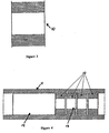
- Figures 3 and 4 show how spools 10 of dispersion compensating fibre used for the dispersion compensation elements may be--fitted within the sea-casing 11 of a submarine optical repeater.
- the outside diameter of the spool 10 is selected to fit within the internal diameter of a standard sea-casing 11, typically around 200mm.
- the internal diameter of the spool is selected to match the minimum bend radius of the optical fibre, which is typically around 50mm.
- the height of each spool 10 varies according to the length of fibre used for the dispersion compensation element. Typically, 50km sections may be used, requiring a spool height of around 100mm.
- the spools 10 are arranged at one end of the casing to leave a space 12 at the other end for a number of opto-electronics trays which implement various other functions associated with optical repeaters.
- the bore of the spools 10 provides a passage 13 for other optical, electrical and mechanical elements.
- FIG. 5 shows another example of a dispersion compensation device 20 according to the present invention.
- the device 20 consists of an optical circulator 21 connected to an optical input 22.
- An optical arm branches from one of the ports of the optical circulator to couple a WDM signal received at the optical input 22 to a band selective dispersion compensation element 23.
- the band selective dispersion compensation element 23 may be a photorefractive element or diffraction grating.
- a mirror 24 forming a bulk reflector.
- the optical circulator 21 couples signals reflected by both the band selective dispersion compensation element 23 and the reflector 24 to an optical output 25.
- the entire WDM signal received at the optical input is coupled via the arm to the dispersion compensation element 23 which applies a wavelength dependent delay to in-band channels and reflects them to the optical output of the optical circulator 21.
- Out-of-band channels are coupled to the bulk reflector 24 and hence back to the same optical output.
- a bulk delay may be imposed on out-of-band channels by the additional propagation path length provided by the length of optical fibre. This delay may be chosen to provide inter-band dispersion compensation. It may also be minimised, to be negligible.
- this dispersion compensation device 20 applies a dispersion compensation accumulation slope to channels of the WDM signal which lie within the predetermined band affected by the dispersion compensating element 23. Channels outside this band are unaffected, apart from a uniform delay imposed by the (optional) additional optical path to and from the bulk reflector.
- FIG 6 shows a cascaded arrangement for applying dispersion compensation to two wavelength bands.
- This scheme consists of two of the band selective dispersion compensation devices 20 shown in Figure 5, in which each of the dispersion compensation elements 23 are selected to compensate different wavelength bands. Any number of the devices 20 can be cascaded to cover the entire bandwidth of a WDM signal to apply compensation to groups of channels. The length of the optical path in each case may be adjusted to provide an extra degree of freedom for relative dispersion compensation between bands. This is in addition to the dispersion compensation within the bands provided by the dispersion compensation elements 23.
- FIG 7 illustrates the effect of the two-layer cascade shown in Figure 6, where dispersion compensation has been applied to both bands.
- band 1 has been relatively delayed and band 2 has been relatively advanced. Within each wavelength band, longer wavelengths have been relatively delayed.
- Figure 8 shows an example of how the dispersion compensation devices of the present invention may be used in a submarine communications system. Dispersion compensation devices within optical repeaters are placed at regular intervals along the length of the submarine cable to process optical signals.
Landscapes
- Physics & Mathematics (AREA)
- Electromagnetism (AREA)
- Engineering & Computer Science (AREA)
- Computer Networks & Wireless Communication (AREA)
- Signal Processing (AREA)
- Optical Communication System (AREA)
- Diffracting Gratings Or Hologram Optical Elements (AREA)
Claims (21)
- Verfähren einer Dispersionskompensation mit folgenden Schritten:Empfangen eines optischen Signals mit einer Reihe von Kanälen, welche durch Wellenlängen separatisiert werden; undAnwenden der Dispersionskompensation auf mindestens einem optischen Übertragungsweg; dadurch gekennzeichnet, dass dieser Übertragungsweg ein Wellenlängen-Frequenzband trägt, welches eine Vielzahl von Kanälen umspannt, und welches weniger als die Gesamtzahl der Kanäle in dem optischen Signal ergibt, mit dem die Dispersionskompensation auf das Wellenlängen-Frequenzband appliziert wird, und das von den Wellenlängen außerhalb des Wellenlängen-Frequenzbandes unabhängig ist.
- Verfahren nach Anspruch 1, welches zusätzlich die folgenden Schritte aufweist:Splitten einer Vielzahl von Kanälen in zwei oder mehreren Wellenlängen-Frequenzbändern;Übertragungs-Ausbreitung von zwei oder der mehreren Wellenlängen-Frequenzbändern entlang getrennter, optischer Übertragungswege, wobei die Dispersionskompensation in mindestens einem der optischen Übertragungswege appliziert wird, und anschließendesNeukombinieren der Signale an einem optischen Ausgang.
- Verfahren nach Anspruch 2, wobei das auf mindestens einem der optischen Übertragungswege übertragene Signal verstärkt wird, um Übertragungsverluste kompensieren zu können.
- Verfahren nach einem der vorstehenden Ansprüche, wobei die Dispersionskompensation mittels einer Vielzahl von Längen der optischen Dispersionskompensations-Glasfaser bereitgestellt wird.
- Verfahren nach Anspruch 1, welches die folgenden Schritte umfasst:Passieren des gesamten optischen Signals durch ein bandselektives Dispersionskompensationsmittel, das einzig zur Applikation der Dispersionskompensation auf Kanäle innerhalb eines voreingestellten Wellenlängen-Frequenzbandes adaptiert ist.
- Verfahren nach Anspruch 5, wobei die Kanäle außerhalb des voreingestellten Wellenlängen-Frequenzbandes durch ein optisches Element reflektiert werden, welches anders als das bandselektive Dispersionskompensationsmittel ist.
- Verfahren nach Anspruch 5 oder 6, wobei das Dispersionskompensationsmittel ein Photorefraktionselement oder ein Beugungsgitter ist.
- Verfahren nach einem der vorstehenden Ansprüche, welches zusätzlich die folgenden Schritte aufweist:Formatbildung einer gleichförmigen Zeitverzögerung auf ein spezielles Wellenlängen-Frequenzband, um die relative Dispersion zwischen dem speziellen Wellenlängen-Frequenzband und einem zweiten unterschiedlichen Wellen-Frequenzband zu kompensieren.
- Dispersionskompensations-Vorrichtung für die Anwendung der Dispersionskompensation auf ein optisches Signal mit einer Reihe von Kanälen, welche ein Dispersionskompensationsmittel (6, 7, 23) aufweist, das so konfiguriert ist, um die Dispersionskompensation auf mindestens einem optischen Übertragungsweg anzuwenden; dadurch gekennzeichnet dass, der Übertragungsweg ein voreingestelltes Wellenlängen-Frequenzband überträgt, welches eine Vielzahl von Kanälen umspannt, und welches weniger als die Gesamtzahl der Kanäle aus dem optischen Signal ergibt, mit dem die Dispersionskompensation auf das voreingestellte Wellenlängen-Frequenzband appliziert wird, das von den Wellenlängen außerhalb des voreingestellten Wellenlängen-Frequenzbandes unabhängig ist.
- Vorrichtung nach Anspruch 9, welche zusätzlich einen Frequenzband-Splitter umfasst, der so angeordnet ist, um zwei oder mehrere optische Übertragungswege zu beschicken, wobei mindestens einer der optischen Übertragungswege ein Dispersionskompensationsmittel aufweist.
- Vorrichtung nach Anspruch 9 oder 10, in welcher das Dispersionskompensationsmittel die Länge der optischen Dispersionskompensations-Glasfaser aufweist.
- Vorrichtung nach einem der Ansprüche 9 bis 11, welche zusätzlich einen optoelektronischen Koppler aufweist, der so angeordnet ist, um ein optisches Signal, das an einem optischen Eingang empfangen worden ist, auf einen optischen Übertragungsweg mit einem Dispersionskompensationsmittel einzuspeisen, wobei das Dispersionskompensationsmittel so adaptiert ist, damit die Dispersionskompensation auf einer Reihe von Kanälen innerhalb einer limitierten Frequenz-Bandbreite angewendet werden kann, und um die Signale innerhalb dieser Bandbreite an einen optischen Ausgang des optoelektronischen Kopplers zu reflektieren.
- Vorrichtung nach Anspruch 12, in welcher der optoelektronische Koppler ein optischer Zirkulator ist.
- Vorrichtung nach einem der Ansprüche 9 bis 13, in welcher das Dispersionskompensationsmittel ein Beugungsgitter ist.
- Vorrichtung nach einem der Ansprüche 9 bis 13, in welcher das Dispersionskompensationsmittel ein Photorefraktionselement ist.
- Vorrichtung nach einem der Ansprüche 12 bis 15, in welcher die Dispersionskompensations-Vorrichtung zusätzlich einen optischen Reflektor aufweist, der an das Dispersionskompensationsmittel gekoppelt ist, um optische Signale von außerhalb der voreingestellten Frequenz-Bandbreite an den optischen Ausgang des optoelektronischen Kopplers zu reflektieren.
- Vorrichtung nach einem der Ansprüche 9 bis 16, welche zusätzlich ein Zeitverzögerungselement aufweist, um eine Innerband-Dispersionskompensation zur Verfügung stellen zu können.
- Vorrichtung nach Anspruch 16 oder Anspruch 17, wenn dieser von Anspruch 16 abhängig ist, in welcher das Zeitverzögerungselement eine Länge der optischen Glasfaser ist, das zwischen dem Dispersionskompensationsmittel und dem optischen Reflektor gekoppelt ist.
- Dispersionskompensations-Vorrichtung nach einem der Ansprüche 9 bis 18, welche ein Gehäuse mit mindestens einem Spulenkörper der Dispersionskompensations-Glasfaser umfasst, der innerhalb des Gehäuses so axial ausgerichtet ist, um einen Durchlauf bereit zu stellen, welcher sich entlang einer Länge des Gehäuseteils durch den Kern des Spulenkörpers erstreckt.
- Vorrichtung nach Anspruch 19, in welcher das Gehäuse ein Unterwassergehäuse ist.
- Vorrichtung nach Anspruch 20, in welcher das Unterwassergehäuse die Ummantelung für einen Optikregenerator ist.
Applications Claiming Priority (2)
| Application Number | Priority Date | Filing Date | Title |
|---|---|---|---|
| GBGB0002286.3A GB0002286D0 (en) | 2000-02-01 | 2000-02-01 | Optical dispersion compensation |
| GB0002286 | 2000-02-01 |
Publications (2)
| Publication Number | Publication Date |
|---|---|
| EP1122899A1 EP1122899A1 (de) | 2001-08-08 |
| EP1122899B1 true EP1122899B1 (de) | 2003-07-02 |
Family
ID=9884746
Family Applications (1)
| Application Number | Title | Priority Date | Filing Date |
|---|---|---|---|
| EP01300637A Expired - Lifetime EP1122899B1 (de) | 2000-02-01 | 2001-01-24 | Optische Dispersionskompensation |
Country Status (6)
| Country | Link |
|---|---|
| US (1) | US20020012147A1 (de) |
| EP (1) | EP1122899B1 (de) |
| JP (1) | JP4426732B2 (de) |
| AT (1) | ATE244477T1 (de) |
| DE (1) | DE60100407T2 (de) |
| GB (1) | GB0002286D0 (de) |
Families Citing this family (7)
| Publication number | Priority date | Publication date | Assignee | Title |
|---|---|---|---|---|
| US20030175032A1 (en) * | 2002-03-15 | 2003-09-18 | Ranalli Eliseo R. | Planar device having an IIR tapped delay line for multiple channel dispersion and slope compensation |
| US7239783B2 (en) * | 2002-07-01 | 2007-07-03 | Sumitomo Electric Industries, Ltd. | Optical fiber, dispersion compensator, and optical transmission system |
| US7206484B2 (en) * | 2002-07-01 | 2007-04-17 | Sumitomo Electric Industries, Ltd. | Optical fiber, dispersion compensator, and optical transmission system |
| JP4952744B2 (ja) * | 2009-06-15 | 2012-06-13 | 富士通株式会社 | 可変波長分散補償器および光受信モジュール |
| US8449814B2 (en) * | 2009-08-07 | 2013-05-28 | Paul V. Cooper | Systems and methods for melting scrap metal |
| EP2648352B1 (de) * | 2012-04-05 | 2016-03-30 | Alcatel Lucent | Verfahren zum Ausgleichen einer chromatischen Verteilung und zugehöriges Gerät |
| US9960849B1 (en) * | 2016-12-22 | 2018-05-01 | Intel Corporation | Channelization for dispersion limited waveguide communication channels |
Family Cites Families (8)
| Publication number | Priority date | Publication date | Assignee | Title |
|---|---|---|---|---|
| US5473719A (en) * | 1993-11-15 | 1995-12-05 | At&T Corp. | Optical dispersion compensator |
| EP0684709B1 (de) * | 1994-05-25 | 2002-10-02 | AT&T Corp. | Optisches Übertragungssystem mit verstellbarer Dispersionskompensation |
| EP0732819A3 (de) * | 1995-03-15 | 1998-03-11 | Sumitomo Electric Industries, Ltd. | Farbzerstreuungskompensator und farbstreuungskompensierendes optisches Übertragungssystem |
| JPH08256106A (ja) * | 1995-03-17 | 1996-10-01 | Fujitsu Ltd | 光増幅海底伝送システムの分散補償装置 |
| JPH09191290A (ja) * | 1996-01-10 | 1997-07-22 | Nec Corp | 光伝送路の波長分散補償システム |
| IT1283405B1 (it) * | 1996-03-11 | 1998-04-21 | Pirelli Cavi S P A Ora Pirelli | Metodo di compensazione selettiva della dispersione cromatica di segnali ottici |
| US6137604A (en) * | 1996-12-04 | 2000-10-24 | Tyco Submarine Systems, Ltd. | Chromatic dispersion compensation in wavelength division multiplexed optical transmission systems |
| KR100302634B1 (ko) * | 1998-12-10 | 2001-11-30 | 서평원 | Wdm광채널을모니터링하고분산을보상하는모듈및그모듈을포함한광증폭기 |
-
2000
- 2000-02-01 GB GBGB0002286.3A patent/GB0002286D0/en not_active Ceased
-
2001
- 2001-01-24 EP EP01300637A patent/EP1122899B1/de not_active Expired - Lifetime
- 2001-01-24 AT AT01300637T patent/ATE244477T1/de not_active IP Right Cessation
- 2001-01-24 DE DE60100407T patent/DE60100407T2/de not_active Expired - Lifetime
- 2001-01-25 JP JP2001017051A patent/JP4426732B2/ja not_active Expired - Lifetime
- 2001-01-30 US US09/771,660 patent/US20020012147A1/en not_active Abandoned
Also Published As
| Publication number | Publication date |
|---|---|
| JP2001292101A (ja) | 2001-10-19 |
| EP1122899A1 (de) | 2001-08-08 |
| ATE244477T1 (de) | 2003-07-15 |
| DE60100407T2 (de) | 2004-04-15 |
| GB0002286D0 (en) | 2000-03-22 |
| US20020012147A1 (en) | 2002-01-31 |
| JP4426732B2 (ja) | 2010-03-03 |
| DE60100407D1 (de) | 2003-08-07 |
Similar Documents
| Publication | Publication Date | Title |
|---|---|---|
| US5633741A (en) | Multichannel optical fiber communications | |
| US6185023B1 (en) | Optical add-drop multiplexers compatible with very dense WDM optical communication systems | |
| US6459516B1 (en) | Dense WDM add/drop multiplexer | |
| US6259555B1 (en) | Multi-band amplification system for dense wavelength division multiplexing | |
| CA2345181C (en) | Bi-directional optical transmission using dual channel bands | |
| US7376355B2 (en) | Optical transmission apparatus and optical transmission system | |
| US6563978B2 (en) | Optical transmission system and optical coupler/branching filter | |
| JP2002518696A (ja) | 光学伝播システムにおいて光学チャンネルをドロップするための方法及び装置 | |
| US6559988B1 (en) | Optical wavelength add/drop multiplexer for dual signal transmission rates | |
| EP1122899B1 (de) | Optische Dispersionskompensation | |
| US6473540B1 (en) | Device and method for filtering optical wavelengths | |
| US6516112B1 (en) | Optical wavelength filter and demultiplexer | |
| EP3614581A1 (de) | Bidirektionales optisches übertragungssystem und bidirektionales optisches übertragungsverfahren | |
| US6552834B2 (en) | Methods and apparatus for preventing deadbands in an optical communication system | |
| US7130542B2 (en) | Modular multiplexing/demultiplexing units in optical transmission systems | |
| JP2002101045A (ja) | 波長分散補償装置及び光伝送路 | |
| US7209662B2 (en) | Wavelength multiplex transmission device | |
| JP2002221742A (ja) | ラマン増幅中継器およびラマン増幅中継伝送システム | |
| US6549701B1 (en) | Selectable wavelength channel filter for optical WDM systems | |
| US7031613B1 (en) | Chromatic dispersion compensation by sub-band | |
| US20020027685A1 (en) | Bidirectional add/drop multiplexer | |
| JPH10170752A (ja) | 分散補償光回路 | |
| CN223744729U (zh) | 一种可扩展O band波长信号的密集波分复用传输系统 | |
| EP4138316B1 (de) | Halbleiterbasiertes system und verfahren zur breitbandübertragung | |
| JP2007532018A (ja) | モジュール式分散補償器 |
Legal Events
| Date | Code | Title | Description |
|---|---|---|---|
| PUAI | Public reference made under article 153(3) epc to a published international application that has entered the european phase |
Free format text: ORIGINAL CODE: 0009012 |
|
| AK | Designated contracting states |
Kind code of ref document: A1 Designated state(s): AT BE CH CY DE DK ES FI FR GB GR IE IT LI LU MC NL PT SE TR |
|
| AX | Request for extension of the european patent |
Free format text: AL;LT;LV;MK;RO;SI |
|
| 17P | Request for examination filed |
Effective date: 20010924 |
|
| 17Q | First examination report despatched |
Effective date: 20011129 |
|
| AKX | Designation fees paid |
Free format text: AT BE CH CY DE DK ES FI FR GB GR IE IT LI LU MC NL PT SE TR |
|
| GRAH | Despatch of communication of intention to grant a patent |
Free format text: ORIGINAL CODE: EPIDOS IGRA |
|
| GRAH | Despatch of communication of intention to grant a patent |
Free format text: ORIGINAL CODE: EPIDOS IGRA |
|
| GRAA | (expected) grant |
Free format text: ORIGINAL CODE: 0009210 |
|
| AK | Designated contracting states |
Designated state(s): AT BE CH CY DE DK ES FI FR GB GR IE IT LI LU MC NL PT SE TR |
|
| PG25 | Lapsed in a contracting state [announced via postgrant information from national office to epo] |
Ref country code: CH Free format text: LAPSE BECAUSE OF FAILURE TO SUBMIT A TRANSLATION OF THE DESCRIPTION OR TO PAY THE FEE WITHIN THE PRESCRIBED TIME-LIMIT Effective date: 20030702 Ref country code: LI Free format text: LAPSE BECAUSE OF FAILURE TO SUBMIT A TRANSLATION OF THE DESCRIPTION OR TO PAY THE FEE WITHIN THE PRESCRIBED TIME-LIMIT Effective date: 20030702 Ref country code: FI Free format text: LAPSE BECAUSE OF FAILURE TO SUBMIT A TRANSLATION OF THE DESCRIPTION OR TO PAY THE FEE WITHIN THE PRESCRIBED TIME-LIMIT Effective date: 20030702 Ref country code: BE Free format text: LAPSE BECAUSE OF FAILURE TO SUBMIT A TRANSLATION OF THE DESCRIPTION OR TO PAY THE FEE WITHIN THE PRESCRIBED TIME-LIMIT Effective date: 20030702 Ref country code: CY Free format text: LAPSE BECAUSE OF FAILURE TO SUBMIT A TRANSLATION OF THE DESCRIPTION OR TO PAY THE FEE WITHIN THE PRESCRIBED TIME-LIMIT Effective date: 20030702 Ref country code: NL Free format text: LAPSE BECAUSE OF FAILURE TO SUBMIT A TRANSLATION OF THE DESCRIPTION OR TO PAY THE FEE WITHIN THE PRESCRIBED TIME-LIMIT Effective date: 20030702 Ref country code: AT Free format text: LAPSE BECAUSE OF FAILURE TO SUBMIT A TRANSLATION OF THE DESCRIPTION OR TO PAY THE FEE WITHIN THE PRESCRIBED TIME-LIMIT Effective date: 20030702 Ref country code: TR Free format text: LAPSE BECAUSE OF FAILURE TO SUBMIT A TRANSLATION OF THE DESCRIPTION OR TO PAY THE FEE WITHIN THE PRESCRIBED TIME-LIMIT Effective date: 20030702 |
|
| REG | Reference to a national code |
Ref country code: GB Ref legal event code: FG4D |
|
| REG | Reference to a national code |
Ref country code: CH Ref legal event code: EP |
|
| REG | Reference to a national code |
Ref country code: IE Ref legal event code: FG4D |
|
| REF | Corresponds to: |
Ref document number: 60100407 Country of ref document: DE Date of ref document: 20030807 Kind code of ref document: P |
|
| PG25 | Lapsed in a contracting state [announced via postgrant information from national office to epo] |
Ref country code: PT Free format text: LAPSE BECAUSE OF FAILURE TO SUBMIT A TRANSLATION OF THE DESCRIPTION OR TO PAY THE FEE WITHIN THE PRESCRIBED TIME-LIMIT Effective date: 20031002 Ref country code: DK Free format text: LAPSE BECAUSE OF FAILURE TO SUBMIT A TRANSLATION OF THE DESCRIPTION OR TO PAY THE FEE WITHIN THE PRESCRIBED TIME-LIMIT Effective date: 20031002 Ref country code: SE Free format text: LAPSE BECAUSE OF FAILURE TO SUBMIT A TRANSLATION OF THE DESCRIPTION OR TO PAY THE FEE WITHIN THE PRESCRIBED TIME-LIMIT Effective date: 20031002 Ref country code: GR Free format text: LAPSE BECAUSE OF FAILURE TO SUBMIT A TRANSLATION OF THE DESCRIPTION OR TO PAY THE FEE WITHIN THE PRESCRIBED TIME-LIMIT Effective date: 20031002 |
|
| PG25 | Lapsed in a contracting state [announced via postgrant information from national office to epo] |
Ref country code: ES Free format text: LAPSE BECAUSE OF FAILURE TO SUBMIT A TRANSLATION OF THE DESCRIPTION OR TO PAY THE FEE WITHIN THE PRESCRIBED TIME-LIMIT Effective date: 20031013 |
|
| NLV1 | Nl: lapsed or annulled due to failure to fulfill the requirements of art. 29p and 29m of the patents act | ||
| REG | Reference to a national code |
Ref country code: CH Ref legal event code: PL |
|
| ET | Fr: translation filed | ||
| PG25 | Lapsed in a contracting state [announced via postgrant information from national office to epo] |
Ref country code: LU Free format text: LAPSE BECAUSE OF NON-PAYMENT OF DUE FEES Effective date: 20040124 |
|
| PG25 | Lapsed in a contracting state [announced via postgrant information from national office to epo] |
Ref country code: IE Free format text: LAPSE BECAUSE OF NON-PAYMENT OF DUE FEES Effective date: 20040126 |
|
| PG25 | Lapsed in a contracting state [announced via postgrant information from national office to epo] |
Ref country code: MC Free format text: LAPSE BECAUSE OF NON-PAYMENT OF DUE FEES Effective date: 20040131 |
|
| PLBE | No opposition filed within time limit |
Free format text: ORIGINAL CODE: 0009261 |
|
| STAA | Information on the status of an ep patent application or granted ep patent |
Free format text: STATUS: NO OPPOSITION FILED WITHIN TIME LIMIT |
|
| 26N | No opposition filed |
Effective date: 20040405 |
|
| REG | Reference to a national code |
Ref country code: IE Ref legal event code: MM4A |
|
| REG | Reference to a national code |
Ref country code: FR Ref legal event code: CD |
|
| REG | Reference to a national code |
Ref country code: GB Ref legal event code: 732E Free format text: REGISTERED BETWEEN 20131114 AND 20131120 |
|
| REG | Reference to a national code |
Ref country code: DE Ref legal event code: R082 Ref document number: 60100407 Country of ref document: DE Representative=s name: DREISS PATENTANWAELTE PARTNERSCHAFT, DE Ref country code: DE Ref legal event code: R082 Ref document number: 60100407 Country of ref document: DE Representative=s name: BARDEHLE PAGENBERG PARTNERSCHAFT PATENTANWAELT, DE Ref country code: DE Ref legal event code: R082 Ref document number: 60100407 Country of ref document: DE Representative=s name: BARDEHLE PAGENBERG PARTNERSCHAFT MBB PATENTANW, DE |
|
| REG | Reference to a national code |
Ref country code: FR Ref legal event code: CA Effective date: 20131219 |
|
| REG | Reference to a national code |
Ref country code: DE Ref legal event code: R082 Ref document number: 60100407 Country of ref document: DE Representative=s name: BARDEHLE PAGENBERG PARTNERSCHAFT PATENTANWAELT, DE Ref country code: DE Ref legal event code: R082 Ref document number: 60100407 Country of ref document: DE Representative=s name: BARDEHLE PAGENBERG PARTNERSCHAFT MBB PATENTANW, DE |
|
| REG | Reference to a national code |
Ref country code: GB Ref legal event code: 732E Free format text: REGISTERED BETWEEN 20140501 AND 20140507 |
|
| REG | Reference to a national code |
Ref country code: DE Ref legal event code: R079 Ref document number: 60100407 Country of ref document: DE Free format text: PREVIOUS MAIN CLASS: H04B0010180000 Ipc: H04B0010250700 |
|
| REG | Reference to a national code |
Ref country code: FR Ref legal event code: TP Owner name: QUALCOMM INCORPORATED, US Effective date: 20140519 |
|
| REG | Reference to a national code |
Ref country code: DE Ref legal event code: R082 Ref document number: 60100407 Country of ref document: DE Representative=s name: BARDEHLE PAGENBERG PARTNERSCHAFT MBB PATENTANW, DE Effective date: 20140120 Ref country code: DE Ref legal event code: R081 Ref document number: 60100407 Country of ref document: DE Owner name: QUALCOMM INCORPORATED, SAN DIEGO, US Free format text: FORMER OWNER: ALCATEL LUCENT, PARIS, FR Effective date: 20140120 Ref country code: DE Ref legal event code: R079 Ref document number: 60100407 Country of ref document: DE Free format text: PREVIOUS MAIN CLASS: H04B0010180000 Ipc: H04B0010250700 Effective date: 20140610 Ref country code: DE Ref legal event code: R082 Ref document number: 60100407 Country of ref document: DE Representative=s name: BARDEHLE PAGENBERG PARTNERSCHAFT MBB PATENTANW, DE Effective date: 20140207 |
|
| REG | Reference to a national code |
Ref country code: FR Ref legal event code: GC Effective date: 20140717 |
|
| REG | Reference to a national code |
Ref country code: FR Ref legal event code: RG Effective date: 20141016 |
|
| REG | Reference to a national code |
Ref country code: FR Ref legal event code: RG Effective date: 20141223 |
|
| REG | Reference to a national code |
Ref country code: FR Ref legal event code: PLFP Year of fee payment: 16 |
|
| REG | Reference to a national code |
Ref country code: FR Ref legal event code: PLFP Year of fee payment: 17 |
|
| REG | Reference to a national code |
Ref country code: FR Ref legal event code: PLFP Year of fee payment: 18 |
|
| PGFP | Annual fee paid to national office [announced via postgrant information from national office to epo] |
Ref country code: FR Payment date: 20191226 Year of fee payment: 20 |
|
| PGFP | Annual fee paid to national office [announced via postgrant information from national office to epo] |
Ref country code: DE Payment date: 20191218 Year of fee payment: 20 Ref country code: GB Payment date: 20191231 Year of fee payment: 20 Ref country code: IT Payment date: 20200116 Year of fee payment: 20 |
|
| REG | Reference to a national code |
Ref country code: DE Ref legal event code: R071 Ref document number: 60100407 Country of ref document: DE |
|
| REG | Reference to a national code |
Ref country code: GB Ref legal event code: PE20 Expiry date: 20210123 |
|
| PG25 | Lapsed in a contracting state [announced via postgrant information from national office to epo] |
Ref country code: GB Free format text: LAPSE BECAUSE OF EXPIRATION OF PROTECTION Effective date: 20210123 |