EP1122922B1 - Circuit d'attaque de ligne à impédance de sortie adaptative - Google Patents
Circuit d'attaque de ligne à impédance de sortie adaptative Download PDFInfo
- Publication number
- EP1122922B1 EP1122922B1 EP01300323A EP01300323A EP1122922B1 EP 1122922 B1 EP1122922 B1 EP 1122922B1 EP 01300323 A EP01300323 A EP 01300323A EP 01300323 A EP01300323 A EP 01300323A EP 1122922 B1 EP1122922 B1 EP 1122922B1
- Authority
- EP
- European Patent Office
- Prior art keywords
- current
- circuit
- signal
- buffer
- output
- Prior art date
- Legal status (The legal status is an assumption and is not a legal conclusion. Google has not performed a legal analysis and makes no representation as to the accuracy of the status listed.)
- Expired - Lifetime
Links
Images




Classifications
-
- H—ELECTRICITY
- H04—ELECTRIC COMMUNICATION TECHNIQUE
- H04L—TRANSMISSION OF DIGITAL INFORMATION, e.g. TELEGRAPHIC COMMUNICATION
- H04L25/00—Baseband systems
- H04L25/02—Details ; arrangements for supplying electrical power along data transmission lines
- H04L25/0264—Arrangements for coupling to transmission lines
- H04L25/0266—Arrangements for providing Galvanic isolation, e.g. by means of magnetic or capacitive coupling
-
- H—ELECTRICITY
- H04—ELECTRIC COMMUNICATION TECHNIQUE
- H04L—TRANSMISSION OF DIGITAL INFORMATION, e.g. TELEGRAPHIC COMMUNICATION
- H04L25/00—Baseband systems
- H04L25/02—Details ; arrangements for supplying electrical power along data transmission lines
- H04L25/0264—Arrangements for coupling to transmission lines
- H04L25/0278—Arrangements for impedance matching
-
- H—ELECTRICITY
- H04—ELECTRIC COMMUNICATION TECHNIQUE
- H04L—TRANSMISSION OF DIGITAL INFORMATION, e.g. TELEGRAPHIC COMMUNICATION
- H04L25/00—Baseband systems
- H04L25/02—Details ; arrangements for supplying electrical power along data transmission lines
- H04L25/0264—Arrangements for coupling to transmission lines
- H04L25/028—Arrangements specific to the transmitter end
-
- H—ELECTRICITY
- H04—ELECTRIC COMMUNICATION TECHNIQUE
- H04L—TRANSMISSION OF DIGITAL INFORMATION, e.g. TELEGRAPHIC COMMUNICATION
- H04L25/00—Baseband systems
- H04L25/02—Details ; arrangements for supplying electrical power along data transmission lines
- H04L25/0264—Arrangements for coupling to transmission lines
- H04L25/0272—Arrangements for coupling to multiple lines, e.g. for differential transmission
Definitions
- the present invention relates to a line driver having a self adjustable output impedance and, in particular, to a transformer line driver.
- FIGURE 1A A simplified schematic of one such driver 10 is illustrated in FIGURE 1A.
- the driver 10 (also referred to as a 'buffer”) comprises an operational amplifier 12 whose negative input terminal receives an input voltage Vin.
- the output terminal of the operational amplifier 12 is connected to the gates of two field effect transistors 14 and 16, where the illustrated "N" value is equal to the ratio of their respective drain currents.
- the sources of the field effect transistors 14 and 16 are connected to a reference voltage Vdd.
- the drains of the field effect transistors 14 and 16 are connected to each other by a resistor (R1) 18.
- the drain of the field effect transistor 14 is connected in a feedback fashion to the positive input terminal of the operational amplifier 12, and is also connected to ground through a resistor (R2) 20.
- An output voltage Vout is supplied from the drain of the field effect transistor 16 to drive a transmission line 22 having a characteristic resistance equal to the load resistance (RL) 24.
- the value of the output impedance from the driver may be set (i.e., controlled) substantially equal to the load resistance RL.
- An advantage of this driver is its reduced power dissipation which makes it very attractive for implementation in an integrated circuit.
- the precise resistance values needed to achieve substantial matching of driver-line impedance are very difficult to consistently obtain.
- the driver of FIGURE 1A may be modified, as shown in FIGURE 1B, to provide for such an adjustment mechanism.
- Controllable source degeneration (through circuit 30) is applied to the transistors 14 and 16.
- the current ratio value "N" is electrically tunable (through circuit 30) via application of the voltage Vtune.
- the driver adapts to match the load resistance RL using a control loop 28 that integrates the output current from the transistor 16 to generate Vtune for application to circuit 30 resulting in an adjustment to the source current of transistor 14 and a change in the value of N.
- control loop 28 forces Vout to equal Vin, in which case the gain of the driver is one.
- the control loop 28 By then setting the resistances R1 and R2 as discussed above, approximate matching of the output impedance to the load resistance RL is obtained, with the control loop 28 further refining the matching.
- transformer driver-line decoupling is utilized in the push-pull configuration, a direct current output signal related to the load resistance is not available to be integrated by the control loop 28 and produce the adjustment signal Vtune. Furthermore, if the transmission line is relatively long, its direct current resistance is substantially different from the characteristic impedance. In such situations, the precision of the impedance adjustment provided by the FIGURE 1B circuit is not sufficient. Additionally, the FIGURE 1A prior art driver has not, historically, been well suited for use in a push-pull B-class circuit as two such drivers are needed and they do not operate well together in push-pull.
- one half of the push-pull circuit i.e., one driver 10
- one driver When one half of the push-pull circuit (i.e., one driver 10) generates some voltage in one half of the primary coil of the transformer, a flyback voltage appears in the other half of the primary coil. This flyback voltage penetrates to the input of the operational amplifier 12 of the other driver 10 through the feedback circuit connections and corrupts driver operation.
- a line driver circuit comprising: a buffer including an adjustable current source and having a signal input and a signal output that provides a line driver output signal buffered from the signal input, the buffer further including a tuning input connected to the adjustable current source; and a tuning circuit, comprising: a first current source producing a first current; a second current source producing a second current; a current mirror having a fixed branch connected to receive the first current and an adjustable branch connected to receive the second current, the current mirror further having a control input to the adjustable branch and having an output; and a comparison circuit receiving the current mirror output for comparison to predetermined limits, the comparison circuit generating a control signal for application to the control input to maintain the current mirror output within the predetermined limits and generating a tuning signal for application to the tuning input of the buffer to adjust operation of the adjustable current source to control an output impedance of the buffer.
- a method for controlling the output impedance of a line driver comprising the steps of: generating a first and second currents; applying the first current to a fixed branch of a current mirror circuit;
- FIGURE 2A a schematic diagram of a push-pull type transformer line driver 40 with adjustable output impedance in accordance with the present invention.
- the driver 40 includes a pair of identical controlled or synthesized impedance buffers 42 (1) and 42(2) whose outputs are connected to the end terminals of a center tapped primary coil 44 of a transformer 46 in a configuration constituting a push-pull circuit.
- Each buffer 42 may comprise the illustrated buffer, a buffer/driver similar or equivalent to that shown in FIGURE 1, or another buffer/driver which provides a controlled or synthesized output impedance preferably with reduced power dissipation characteristics suitable for integrated circuit fabrication.
- Each buffer 42 includes a pair of inputs 48(1) and 48(2). In the specific implementation illustrated these inputs are applied to the negative and positive input terminals, respectively, of the included operational amplifier 12.
- One input 48(1) receives a buffer input signal, while the other input 48(2) receives a flyback compensation signal (the purpose of which will be described later).
- the buffer input signal applied to the first input 48(1) of each buffer 42 provides an input current that is passed through the buffer and output as a line driver signal for application to an end terminal of the center tapped primary coil 44 for the transformer 46. While outputting the line driver signal, the buffer 42 maintains the value of its output impedance for the connection to the transformer 46 in a condition set equal to the characteristic impedance RL of a transmission line (not shown) connected at TX+ and TX-terminals of the secondary coil.
- this line driver signal as applied by one buffer 42 (for example, buffer 42(1)) in such a push-pull configuration to one half of the primary coil induces a flyback voltage in the other half of the primary coil that penetrates (as an unwanted flyback signal) through the other buffer (for example, buffer 42(2), which at that time is inactive) to corrupt driver 40 operation.
- This is especially a concern when a buffer/driver of the prior art FIGURE 1A type (or similar) is used because the unwanted flyback signal may pass through the feedback loop of the buffer to the positive input terminal of the operational amplifier 12.
- the driver 40 further includes a pair of pre-driver circuits 50(1) and 50(2).
- Each pre-driver circuit 50 receives an input signal (Vin in differential +/format) and outputs two signals: a first signal comprising the buffer input signal for application to the first input 48(1) of one of the buffers 42 (for example, buffer 42(1)); and a second signal comprising the flyback compensation signal for application to the second input 48 (2) of the other buffer 42 (for example, buffer 42 (2)) .
- the buffer input signal generated by the first pre-driver 50(1) is applied to the first input 48(1) of the first buffer 42(1)
- the flyback compensation signal generated by the first pre-driver 50(1) is applied to the second input 48(2) of the second buffer 42(2).
- the buffer input signal generated by the second pre-driver 50(2) is applied to the first input 48(1) of the second buffer 42(2) while the flyback compensation signal generated by the second pre-driver 50(2) is applied to the second input 48(2) of the first buffer 42(1).
- the pre-driver may alternatively be implemented as a differential circuit (to process the received driver input voltage signal and generate the appropriate input voltage and flyback compensation signals) instead of having two equivalent pre-drivers 50 (1) and 50(2).
- the flyback compensation signal as generated by the pre-driver 50 is proportional (in current) to the buffer input signal.
- the ratio of the currents for these signals is selected in such a way that current of the flyback voltage induced in the primary coil of the transformer by the adjacent half of the push-pull driver (as represented by the unwanted flyback signal that penetrates through the feedback to the input of the operational amplifier, and due to the applied line driver signal) is substantially equal to current of the generated flyback compensation signal.
- the operation of one buffer 42 does not affect the operation of the other included buffer as these two signals will cancel each other (through a subtraction operation) at the output of the operational amplifier 12.
- Each pre-driver 50 includes a pair of controlled current sources 52(1) and 52(2) that receive the driver input voltage signal and output the input voltage signal and flyback compensation signal.
- the output of the first current source 52(1) is connected to the negative input terminal of the operational amplifier of one buffer 42 (to provide the buffer input signal) and the output of the second current source 52(2) is connected to the positive input terminal of the operational amplifier of the other buffer (to provide the flyback compensation signal).
- the values of the transconductances of the first and second current sources 52(1) and 52(2), respectively, must be properly chosen such that the current of flyback voltage (i.e., the unwanted flyback signal) induced in one half of the primary coil of the transformer by the adjacent half of the push-pull driver will be substantially equal to the generated flyback compensation signal (i.e., to set the appropriate proportional relationship).
- each buffer 42 includes a fixed controlled current source 64 and an adjustable controlled current source 66.
- the adjustable controlled current source 66 receives an adjustment signal (Vtune) output from an impedance adjustment circuit 100.
- the signal Vtune adjusts the current being passed by the source 66, and thus (in comparison to the current of the fixed source 64) affects the value for the current ratio "N".
- the value of the output impedance may be more narrowly focused to match that of the load resistance RL (in a manner similar to that as discussed above in connection with FIGURE 1B).
- the driver 40 operates in substantially perfect impedance matching with the transmission line.
- the impedance adjustment circuit 100 includes two current sources 102(1) and 102(2), a converter 104 and a current mirror 106.
- the current mirror 106 includes an adjustable branch 108 and a fixed branch 110.
- the first current source 102(1) produces a stable current that it derives from the value of a precise reference voltage Vref and a stable precise resistor Rext.
- the second current source 102(2) produces a current that it derives from the value of the resistor Rint.
- the resistor Rint comprises an internal resistor residing in the integrated circuit chip
- the resistor Rext comprises a specially selected resistor residing external to the integrated circuit chip and electrically connected to the pins of the chip.
- the value of the resistor Rint is subject to the same process and temperature variations as the other 'internal" resistors of the line driver (such as those resistors included in thebuffer 42).
- the first current is applied to the input (branch 110) of the current mirror 106.
- the second current is applied to the output (branch 108) of the current mirror 106.
- the converter 104 receives the voltage output from the current mirror 106 (branch 108), compares it to some predetermined upper and lower limits and outputs (as Vtune) a digital code and a residual analog signal indicative of the results of that comparison.
- the converter 104 generated output Vtune accordingly comprises a combined digital/analog output that is applied to the adjustable branch 108 of the current mirror 106 to keep its output signal within some predetermined limits.
- the output Vtune sets the output current from the current mirror 106 equal to the current produced by the second current source 102(2).
- the output Vtune is also applied, as discussed above, to the adjustable controlled current sources 66 of each buffer 42 to tune the value of N (by controlling driver gain) and thus more narrowly focus the value of the output impedance to match that of the load resistance RL.
- the adjustment circuit may be utilized in conjunction with a single buffer having a controlled/controllable output impedance. It is further applicable both to a driver with transformer decoupling (as shown in FIGURE 2A) and a driver with direct coupling to the line (as shown in FIGURE 2B where same reference numbers designate like or similar components).
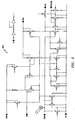
- FIGURES 3-16 wherein there are shown schematic diagrams of one design for the push-pull type transformer line driver 40 of FIGURE 2A as configured for implementation in an integrated circuit.
- FIGURE 3A there is shown a block diagram for the pair of buffers 42.
- the buffers 42 include a plurality of input stages 60 and a plurality of output stages 62.
- the input stages 60 are equivalent to the operational amplifiers 12 for the buffer 42.
- a more detailed schematic of the input stage 60(1) used for operation in 10BASE-T mode is shown in FIGURE 4.
- FIGURE 5 A more detailed schematic of the input stage 60(2) used for operation in 100BASE-TX mode is shown in FIGURE 5.
- FIGURE 6 A more detailed schematic of the output stage 62 is shown in FIGURE 6.
- Each output stage 62 contains a pair of fixed controlled current sources 64 and a pair of adjustable controlled current sources 66. These components perform the same functions as the current sources 14 and 16 for the buffer 42.
- a more detailed schematic of the adjustable controlled current source 66 is shown in FIGURE 7.
- FIGURE 3B illustrates a schematic diagram for a circuit 70 to control the quiescent current of the driver.
- the circuit 70 includes a control circuit 72 whose more detailed schematic diagram is shown in FIGURE 12, plus a pair of input stages 60(1) and 60(2) whose more detailed schematic diagrams are shown in FIGURES 4 and 5, respectively.
- the control circuit 72 of FIGURE 12 includes a pair of adjustable controlled current sources 74 that are identical to the ones (reference 66) shown in FIGURE 6. A more detailed schematic diagram of the circuit 74 is thus shown in FIGURE 7.
- FIGURE 3C illustrates a portion 76 of the adjusting circuit 100 for tuning the output impedance of the drivers 42.
- a more detailed schematic diagram of the circuit portion 76 is shown in FIGURE 13.
- the circuit portion 76 includes inputs 90(1) and 90(2) for receiving the currents derived from the resistors Rext and Rint, respectively.
- the circuit portion 76 further includes the current mirror 106 and the converter 104 comprising an analog voltage follower 94 and a comparison circuit 96.
- a more detailed schematic diagram of the voltage follower 94 is provided in FIGURE 16.
- a more detailed schematic diagram of the comparison circuit 96 is shown in FIGURE 14.
- the comparison circuit 96 comprises a simple asynchronous two bit successive approximation A/D converter.
- the A/D converter contains a top and bottom limit signal generator 120, two comparators 122, two pairs of substantially different delays 124 and 126, and two RS latches 128.
- the least significant bit (LSB) output from one latch 128 for the adjustment signal Vtune is changed first. If this change is enough to move the input signal to within the predetermined limits, then the most significant bit (MSB) output from the other latch is not changed due to the added length of the delay 126. If this LSB change, along with the analog portion of the adjustment signal Vtune output of the voltage follower 94, is not enough to move the input signal to within the predetermined limits, then the MSB output is changed.
- the current mirror 106 includes an adjustable branch 108 having at least one current path 140 that can be turned on/off responsive to a digital control signal output from the latches 128 (of the comparator 96), and at least one current path 142 controlled responsive to an analog control signal output from the voltage follower 94.
- the adjustable controlled current source 66 includes at least one current path 140 that can be turned on/off responsive to a digital control signal output from the latches 128 (of the comparator 96), and at least one current path 142 controlled responsive to an analog control signal output from the voltage follower 94 in order to control the flow of current, directly affect the value "N", and thus maintain the output impedance of the line driver in a matched condition to the transmission line.
- FIGURE 3D illustrates the mode of operation control logic for the driver 42.
- the line driver 40 further includes a pair of pre-drivers 50 whose schematic block diagram is provided in FIGURE 8.
- the pre-driver 50 comprises a current D/A converter that is used for waveshaping of the 10BASE-T and 100BASE-TX driver output signals. It includes a reference current generating block 80, a set of pre-driver D/A converter current cells 82, and a plurality of pre-driver output selecting circuits 84.
- a more detailed schematic diagram of the reference current generating block 80 is shown in-FIGURE 11.
- FIGURE 9 A more detailed schematic diagram of the pre-driver D/A converter current cell 82 is shown in FIGURE 9, which further illustrates that outputs 86 are used as the inputs to one buffer to provide the buffer input signal, and outputs 88 are used as the inputs to the other buffer to provide the flyback compensation signal.
- the cell 82 produces the inputs for either buffer 42(1) or 42(2) in accordance with the commands issued by the pre-driver output selecting circuit 84 whose more detailed circuit diagram is shown in FIGURE 10.
- FIGURE 9 in particular shows that the current cell 82 is capable of simultaneously producing the buffer input signal (from output 86) for one half of the driver 40 and the flyback compensation signal (from outputs 88) for the other half of the driver 40.
Landscapes
- Engineering & Computer Science (AREA)
- Power Engineering (AREA)
- Computer Networks & Wireless Communication (AREA)
- Signal Processing (AREA)
- Logic Circuits (AREA)
- Amplifiers (AREA)
- Control Of Electrical Variables (AREA)
- Dc Digital Transmission (AREA)
Claims (16)
- Circuit d'attaque de ligne (40) comprenant :un tampon (42) comprenant une source de courant réglable (66) ayant une entrée de signal et une sortie de signal qui fournit un signal de sortie pilote de ligne amplifié à partir du signal d'entrée, le tampon (42) comprenant en outre une entrée d'accord (VTUNE) connectée à la source de courant réglable (66) ; etun circuit d'accord (100) comprenant :une première source de courant (102(1)) produisant un premier courant ;une seconde source de courant (102(2)) produisant un second courant ;un miroir de courant (106) ayant une branche fixe (110) connectée pour recevoir le premier courant et une branche réglable (108) connectée pour recevoir le second courant, le miroir de courant (106) ayant en outre une entrée de commande vers la branche réglable et une sortie ; etun circuit de comparaison (104) recevant la sortie du miroir de courant (106) pour comparaison à des limites prédéterminées, le circuit de comparaison (104) produisant un signal de commande (VTUNE) pour l'appliquer à l'entrée de commande pour maintenir la sortie du miroir de courant dans les limites prédéterminées et produisant un signal d'accord (VTUNE) pour l'appliquer à l'entrée de réglage du tampon (42) pour régler le fonctionnement de la source de courant réglable (66) pour commander l'impédance de sortie du tampon (42).
- Circuit d'attaque de ligne selon la revendication 1, disposé pour être connecté à un transformateur (46) ayant un enroulement primaire (44), comprenant en outre un autre tampon (42), tel que les tampons constituent une paire de tampons à impédance équivalente commandée pour connexion en configuration push-pull à l'enroulement primaire (44), chaque tampon (42(1)),42(2)) recevant un signal d'entrée de tampon pour une sortie amplifiée en tant que signal pilote de ligne vers l'enroulement primaire, chaque tampon comprenant en outre une entrée d'accord (VTUNE) connectée à une source de courant réglable (66) dont le fonctionnement assure la commande de l'impédance de sortie du tampon ; d'où il résulte que le circuit d'accord (100) produit un signal d'accord pour l'appliquer à l'entrée d'accord de chaque tampon (42(1),42(2)) pour régler le fonctionnement de la source de courant réglable (66) pour commander l'impédance de sortie du tampon.
- Circuit selon la revendication 1 ou 2, dans lequel le signal d'attaque de ligne est appliqué par l'intermédiaire du transformateur à une ligne de transmission ayant une impédance caractéristique, et dans lequel le signal d'accord (VTUNE) qui règle le fonctionnement de la source de courant réglable (66) commande l'impédance de sortie du tampon pour s'adapter sensiblement à l'impédance caractéristique de la ligne de transmission.
- Circuit selon la revendication 3, dans lequel le tampon est connecté à la ligne de transmission par un transformateur (46).
- Circuit selon la revendication 1 ou 2, dans lequel le signal d'accord (VTUNE) qui règle le fonctionnement de la source de courant réglable (66) commande chaque gain de tampon pour fournir un gain sensiblement unité.
- Circuit selon la revendication 1 ou 2, dans lequel la première source de courant (102(1)) produit le premier courant à partir de la valeur d'une première résistance (REXT) et la seconde source de courant (102(2)) produit le second courant à partir de la valeur d'une seconde résistance (RINT).
- Circuit selon la revendication 6, dans lequel le circuit d'attaque de ligne (40) est fabriqué sur un circuit intégré et la première résistance (REXT) comprend une résistance précise et stable, externe au circuit intégré, et la seconde résistance (RINT) comprend une résistance formée sur le circuit intégré.
- Circuit selon la revendication 1 ou 2, dans lequel le circuit de comparaison comprend un convertisseur analogique-numérique qui produit un signal numérique représentatif du fait que la sortie de la branche réglable est à l'intérieur de limites prédéterminées ou non, le signal numérique étant appliqué en tant que signal de commande à l'entrée de commande pour maintenir la sortie du miroir de courant à l'intérieur des limites prédéterminées.
- Circuit selon la revendication 8, dans lequel la branche réglable (108) du miroir de courant (106) comprend au moins un chemin de courant, et l'entrée de commande comprenant le signal numérique ferme ou ouvre ce chemin de courant.
- Circuit selon la revendication 1 ou 2, dans lequel le circuit de comparaison (104) comprend un générateur de signal analogique qui produit un signal analogique représentatif de la sortie du miroir de courant, le signal analogique étant appliqué en tant que signal de commande à l'entrée de commande pour commander la sortie du miroir de courant.
- Circuit selon la revendication 10, dans lequel la branche réglable (108) du miroir de courant (106) comprend au moins un chemin de courant, et l'entrée de commande, comprenant le signal analogique, commande le courant circulant dans ce chemin de courant.
- Procédé de commande de l'impédance de sortie d'un circuit d'attaque de ligne (40), comprenant les étapes suivantes :produire des premier et second courants ;appliquer le premier courant à une branche fixe (110) d'un circuit de miroir de courant (106) ;appliquer le second courant à une branche réglable (108) du circuit de miroir de courant (106) ;comparer la sortie du circuit de miroir de, courant (106) à des limites prédéterminées pour produire un signal de commande (VTUNE) ;appliquer le signal de commande (VTUNE) à la branche réglable (108) du circuit de miroir de courant (106) pour maintenir la sortie du miroir de courant à l'intérieur des limites prédéterminées ;appliquer le même signal de commande (VTUNE) à une source de courant réglable (66) à l'intérieur du circuit d'attaque de ligne (40) pour maintenir une impédance de sortie du circuit d'attaque de ligne (40) dans un état sensiblement accordé par rapport à une ligne de transmission attaquée.
- Procédé selon la revendication 12, dans lequel l'étape de génération comprend les étapes suivantes :fournir le premier courant à partir de la valeur d'une première résistance (REXT) ; etfournir le second courant à partir de la valeur d'une seconde résistance (RINT).
- Procédé selon la revendication 13, dans lequel le circuit d'attaque de ligne comprend un circuit d'attaque de ligne en circuit intégré, la première résistance (REXT) comprend une résistance précise et stable externe au circuit intégré, et la seconde résistance (RINT) comprend une résistance fabriquée sur le circuit intégré.
- Procédé selon la revendication 12, dans lequel le signal de commande comprend un signal numérique et l'étape d'application du signal de commande à la branche réglable (108) du circuit de miroir de courant (106) comprend l'étape consistant à fermer et ouvrir un chemin de courant de la branche réglable (108).
- Procédé selon la revendication 12, dans lequel le signal de commande comprend un signal analogique et l'étape d'application du signal de commande de la branche réglable (108) du circuit de miroir de courant, (106) comprend l'étape de réglage de la circulation de courant dans un chemin de courant de la branche réglable (108) en réponse au signal analogique.
Applications Claiming Priority (2)
| Application Number | Priority Date | Filing Date | Title |
|---|---|---|---|
| US497980 | 2000-02-04 | ||
| US09/497,980 US6275078B1 (en) | 2000-02-04 | 2000-02-04 | Self-adjustable impendance line driver |
Publications (2)
| Publication Number | Publication Date |
|---|---|
| EP1122922A1 EP1122922A1 (fr) | 2001-08-08 |
| EP1122922B1 true EP1122922B1 (fr) | 2003-08-20 |
Family
ID=23979116
Family Applications (1)
| Application Number | Title | Priority Date | Filing Date |
|---|---|---|---|
| EP01300323A Expired - Lifetime EP1122922B1 (fr) | 2000-02-04 | 2001-01-16 | Circuit d'attaque de ligne à impédance de sortie adaptative |
Country Status (4)
| Country | Link |
|---|---|
| US (1) | US6275078B1 (fr) |
| EP (1) | EP1122922B1 (fr) |
| JP (1) | JP2001268138A (fr) |
| DE (1) | DE60100605T2 (fr) |
Families Citing this family (10)
| Publication number | Priority date | Publication date | Assignee | Title |
|---|---|---|---|---|
| US6542008B1 (en) * | 2000-11-28 | 2003-04-01 | Agere Systems Inc. | System and method for providing an impedance match of an output buffer to a transmission line |
| US6498521B1 (en) * | 2001-11-29 | 2002-12-24 | Lsi Logic Corporation | Dynamic supply control for line driver |
| US20050213783A1 (en) * | 2004-03-29 | 2005-09-29 | Walsh William J | Transmission drive line for low level audio analog electrical signals |
| CN1306703C (zh) * | 2004-04-30 | 2007-03-21 | 华为技术有限公司 | 线驱动器及其控制输出信号的方法 |
| US7609097B2 (en) * | 2004-07-06 | 2009-10-27 | Agere Systems, Inc. | Driver circuit and a method for matching the output impedance of a driver circuit with a load impedance |
| CN100476680C (zh) * | 2006-04-18 | 2009-04-08 | 点晶科技股份有限公司 | 自动换档的电流镜 |
| FR2905211A1 (fr) * | 2006-08-22 | 2008-02-29 | St Microelectronics Sa | Procede et dispositif d'adaptation d'impedance de sortie d'un emetteur. |
| EP2186191A4 (fr) * | 2007-09-06 | 2011-04-20 | Catena Wireless Electronics Inc | Procédé d'utilisation d'amplificateur de puissance intégré |
| US8150074B1 (en) * | 2008-08-08 | 2012-04-03 | Crestron Electronics Inc. | Impedance matching speaker wire system |
| TWI559682B (zh) | 2015-01-14 | 2016-11-21 | 智原科技股份有限公司 | 通過電流調整來調整輸出阻抗以匹配傳輸線阻抗的驅動電路、驅動裝置及方法 |
Family Cites Families (19)
| Publication number | Priority date | Publication date | Assignee | Title |
|---|---|---|---|---|
| NL8602325A (nl) | 1986-09-15 | 1988-04-05 | Philips Nv | Actieve symmetrische balansvorkschakeling. |
| US5121080A (en) | 1990-12-21 | 1992-06-09 | Crystal Semiconductor Corporation | Amplifier with controlled output impedance |
| US5249225A (en) * | 1991-10-25 | 1993-09-28 | Coherent Communications Systems Corp. | Self-balancing hybrid using digitally programmable attenuator for variable impedance elements |
| US5285744A (en) * | 1992-09-04 | 1994-02-15 | Vapor Systems Technologies, Inc. | Coaxial hose assembly |
| GB9308168D0 (en) | 1993-04-20 | 1993-06-02 | Madge Network Limited | Impedance matching |
| TW239239B (fr) * | 1993-07-14 | 1995-01-21 | Philips Electronics Nv | |
| CN1142710A (zh) * | 1994-09-30 | 1997-02-12 | 美国电报电话公司 | 由一个推挽桥式放大器组成的电压信号线路驱动器 |
| US6107867A (en) * | 1994-09-30 | 2000-08-22 | Lucent Technologies Inc. | Load termination sensing circuit |
| US5796276A (en) * | 1994-12-30 | 1998-08-18 | Sgs-Thomson Microelectronics, Inc. | High-side-driver gate drive circuit |
| US5585763A (en) * | 1995-03-30 | 1996-12-17 | Crystal Semiconductor Corporation | Controlled impedance amplifier |
| US5585732A (en) | 1995-06-07 | 1996-12-17 | Mississippi State University | Detector for heterogeneous materials |
| US5757210A (en) * | 1995-08-30 | 1998-05-26 | Cherry Semiconductor Corporation | Comparator with latch |
| US5644258A (en) * | 1996-01-04 | 1997-07-01 | Winbond Electronics Corp. | Driver circuit, with low idle power consumption, for an attachment unit interface |
| US5760601A (en) * | 1996-08-26 | 1998-06-02 | International Business Machines Corporation | Transmission line driver circuit for matching transmission line characteristic impedance |
| US5793223A (en) * | 1996-08-26 | 1998-08-11 | International Business Machines Corporation | Reference signal generation in a switched current source transmission line driver/receiver system |
| US5936393A (en) | 1997-02-25 | 1999-08-10 | U.S. Philips Corporation | Line driver with adaptive output impedance |
| US5973490A (en) | 1997-02-25 | 1999-10-26 | U.S. Philips Corporation | Line driver with adaptive output impedance |
| WO1998038774A2 (fr) * | 1997-02-25 | 1998-09-03 | Koninklijke Philips Electronics N.V. | Circuit d'attaque de ligne a impedance de sortie adaptative |
| WO1998038773A2 (fr) * | 1997-02-25 | 1998-09-03 | Koninklijke Philips Electronics N.V. | Circuit d'attaque de ligne a impedance de sortie adaptative |
-
2000
- 2000-02-04 US US09/497,980 patent/US6275078B1/en not_active Expired - Lifetime
-
2001
- 2001-01-16 EP EP01300323A patent/EP1122922B1/fr not_active Expired - Lifetime
- 2001-01-16 DE DE60100605T patent/DE60100605T2/de not_active Expired - Fee Related
- 2001-02-05 JP JP2001028614A patent/JP2001268138A/ja active Pending
Also Published As
| Publication number | Publication date |
|---|---|
| DE60100605T2 (de) | 2004-06-17 |
| JP2001268138A (ja) | 2001-09-28 |
| US6275078B1 (en) | 2001-08-14 |
| DE60100605D1 (de) | 2003-09-25 |
| EP1122922A1 (fr) | 2001-08-08 |
Similar Documents
| Publication | Publication Date | Title |
|---|---|---|
| US6343024B1 (en) | Self-adjustable impedance line driver with hybrid | |
| CN109845097B (zh) | 具有被耦合的退化电阻和电容的可变增益放大器 | |
| US6806771B1 (en) | Multimode output stage converting differential to single-ended signals using current-mode input signals | |
| US8022736B2 (en) | Line driver with tuned on-chip termination | |
| US7176823B2 (en) | Gigabit ethernet line driver and hybrid architecture | |
| US5789974A (en) | Calibrating the DC-offset of amplifiers | |
| JP3234293B2 (ja) | デジタル利得設定を備えたモノリシック集積差動増幅器 | |
| US20050057315A1 (en) | Ring oscillator with peaking stages | |
| US5510751A (en) | Line driver with adaptive output impedance | |
| US20140049414A1 (en) | Systems and methods for correcting an offset at an output of a digital to analog converter | |
| EP1122922B1 (fr) | Circuit d'attaque de ligne à impédance de sortie adaptative | |
| US9853842B2 (en) | Continuous time linear equalization for current-mode logic with transformer | |
| US6316927B1 (en) | Voltage output driver and filter | |
| US7113121B1 (en) | Communication driver | |
| US7095348B1 (en) | Communication driver | |
| CN117826917A (zh) | 基准电压修调电路 | |
| US5973490A (en) | Line driver with adaptive output impedance | |
| JPH08265115A (ja) | 集積回路 | |
| US7501873B2 (en) | Digitally controlled threshold adjustment circuit | |
| US7148726B2 (en) | Digital signal buffer circuit | |
| JP2790117B2 (ja) | Cmos装置 | |
| US6229396B1 (en) | Controlled impedance transformer line driver | |
| US12113494B2 (en) | Differential amplifier circuit, reception circuit, and semiconductor integrated circuit | |
| USRE41792E1 (en) | Controllable integrator | |
| TWI894739B (zh) | 轉換電路、接收器電路及轉換電路的轉換方法 |
Legal Events
| Date | Code | Title | Description |
|---|---|---|---|
| PUAI | Public reference made under article 153(3) epc to a published international application that has entered the european phase |
Free format text: ORIGINAL CODE: 0009012 |
|
| AK | Designated contracting states |
Kind code of ref document: A1 Designated state(s): DE FR GB IT |
|
| AX | Request for extension of the european patent |
Free format text: AL;LT;LV;MK;RO;SI |
|
| 17P | Request for examination filed |
Effective date: 20020114 |
|
| AKX | Designation fees paid |
Free format text: DE FR GB IT |
|
| 17Q | First examination report despatched |
Effective date: 20020603 |
|
| GRAH | Despatch of communication of intention to grant a patent |
Free format text: ORIGINAL CODE: EPIDOS IGRA |
|
| GRAH | Despatch of communication of intention to grant a patent |
Free format text: ORIGINAL CODE: EPIDOS IGRA |
|
| GRAA | (expected) grant |
Free format text: ORIGINAL CODE: 0009210 |
|
| AK | Designated contracting states |
Designated state(s): DE FR GB IT |
|
| PG25 | Lapsed in a contracting state [announced via postgrant information from national office to epo] |
Ref country code: IT Free format text: LAPSE BECAUSE OF FAILURE TO SUBMIT A TRANSLATION OF THE DESCRIPTION OR TO PAY THE FEE WITHIN THE PRESCRIBED TIME-LIMIT;WARNING: LAPSES OF ITALIAN PATENTS WITH EFFECTIVE DATE BEFORE 2007 MAY HAVE OCCURRED AT ANY TIME BEFORE 2007. THE CORRECT EFFECTIVE DATE MAY BE DIFFERENT FROM THE ONE RECORDED. Effective date: 20030820 |
|
| REG | Reference to a national code |
Ref country code: GB Ref legal event code: FG4D |
|
| REF | Corresponds to: |
Ref document number: 60100605 Country of ref document: DE Date of ref document: 20030925 Kind code of ref document: P |
|
| PGFP | Annual fee paid to national office [announced via postgrant information from national office to epo] |
Ref country code: DE Payment date: 20040219 Year of fee payment: 4 |
|
| ET | Fr: translation filed | ||
| PLBE | No opposition filed within time limit |
Free format text: ORIGINAL CODE: 0009261 |
|
| STAA | Information on the status of an ep patent application or granted ep patent |
Free format text: STATUS: NO OPPOSITION FILED WITHIN TIME LIMIT |
|
| 26N | No opposition filed |
Effective date: 20040524 |
|
| PG25 | Lapsed in a contracting state [announced via postgrant information from national office to epo] |
Ref country code: DE Free format text: LAPSE BECAUSE OF NON-PAYMENT OF DUE FEES Effective date: 20050802 |
|
| PGFP | Annual fee paid to national office [announced via postgrant information from national office to epo] |
Ref country code: GB Payment date: 20070110 Year of fee payment: 7 |
|
| PGFP | Annual fee paid to national office [announced via postgrant information from national office to epo] |
Ref country code: FR Payment date: 20070109 Year of fee payment: 7 |
|
| GBPC | Gb: european patent ceased through non-payment of renewal fee |
Effective date: 20080116 |
|
| REG | Reference to a national code |
Ref country code: FR Ref legal event code: ST Effective date: 20081029 |
|
| PG25 | Lapsed in a contracting state [announced via postgrant information from national office to epo] |
Ref country code: GB Free format text: LAPSE BECAUSE OF NON-PAYMENT OF DUE FEES Effective date: 20080116 |
|
| PG25 | Lapsed in a contracting state [announced via postgrant information from national office to epo] |
Ref country code: FR Free format text: LAPSE BECAUSE OF NON-PAYMENT OF DUE FEES Effective date: 20080131 |