EP1125007B1 - Submikrone metallisierung unter verwendung elektrochemischer beschichtung - Google Patents
Submikrone metallisierung unter verwendung elektrochemischer beschichtung Download PDFInfo
- Publication number
- EP1125007B1 EP1125007B1 EP99954748A EP99954748A EP1125007B1 EP 1125007 B1 EP1125007 B1 EP 1125007B1 EP 99954748 A EP99954748 A EP 99954748A EP 99954748 A EP99954748 A EP 99954748A EP 1125007 B1 EP1125007 B1 EP 1125007B1
- Authority
- EP
- European Patent Office
- Prior art keywords
- electroplating
- current density
- micro
- waveform
- metal
- Prior art date
- Legal status (The legal status is an assumption and is not a legal conclusion. Google has not performed a legal analysis and makes no representation as to the accuracy of the status listed.)
- Expired - Lifetime
Links
- 238000001465 metallisation Methods 0.000 title description 28
- 238000004070 electrodeposition Methods 0.000 title description 3
- 238000000034 method Methods 0.000 claims abstract description 46
- 238000007747 plating Methods 0.000 claims abstract description 44
- 238000009713 electroplating Methods 0.000 claims abstract description 37
- 229910052751 metal Inorganic materials 0.000 claims abstract description 24
- 239000002184 metal Substances 0.000 claims abstract description 24
- 238000000151 deposition Methods 0.000 claims abstract description 22
- 230000008021 deposition Effects 0.000 claims abstract description 15
- 238000004377 microelectronic Methods 0.000 claims abstract description 9
- 229910052802 copper Inorganic materials 0.000 claims description 59
- 239000010949 copper Substances 0.000 claims description 59
- RYGMFSIKBFXOCR-UHFFFAOYSA-N Copper Chemical compound [Cu] RYGMFSIKBFXOCR-UHFFFAOYSA-N 0.000 claims description 58
- 239000004065 semiconductor Substances 0.000 claims description 15
- 239000006259 organic additive Substances 0.000 claims description 10
- 230000002708 enhancing effect Effects 0.000 claims 1
- 239000000654 additive Substances 0.000 abstract description 15
- 230000000996 additive effect Effects 0.000 abstract description 6
- 239000000243 solution Substances 0.000 description 19
- 230000008569 process Effects 0.000 description 18
- 239000000758 substrate Substances 0.000 description 9
- 239000010408 film Substances 0.000 description 7
- 239000004020 conductor Substances 0.000 description 6
- 230000001934 delay Effects 0.000 description 5
- 239000003989 dielectric material Substances 0.000 description 5
- 239000000463 material Substances 0.000 description 5
- 230000000694 effects Effects 0.000 description 4
- 235000012431 wafers Nutrition 0.000 description 4
- 229910000838 Al alloy Inorganic materials 0.000 description 3
- VYPSYNLAJGMNEJ-UHFFFAOYSA-N Silicium dioxide Chemical compound O=[Si]=O VYPSYNLAJGMNEJ-UHFFFAOYSA-N 0.000 description 3
- 238000002474 experimental method Methods 0.000 description 3
- 229910052814 silicon oxide Inorganic materials 0.000 description 3
- XUIMIQQOPSSXEZ-UHFFFAOYSA-N Silicon Chemical compound [Si] XUIMIQQOPSSXEZ-UHFFFAOYSA-N 0.000 description 2
- 230000002378 acidificating effect Effects 0.000 description 2
- 230000004888 barrier function Effects 0.000 description 2
- 230000015572 biosynthetic process Effects 0.000 description 2
- 238000009792 diffusion process Methods 0.000 description 2
- 230000009977 dual effect Effects 0.000 description 2
- 230000006872 improvement Effects 0.000 description 2
- 230000007246 mechanism Effects 0.000 description 2
- 238000005457 optimization Methods 0.000 description 2
- 238000000059 patterning Methods 0.000 description 2
- 229910052710 silicon Inorganic materials 0.000 description 2
- 239000010703 silicon Substances 0.000 description 2
- QPLDLSVMHZLSFG-UHFFFAOYSA-N Copper oxide Chemical compound [Cu]=O QPLDLSVMHZLSFG-UHFFFAOYSA-N 0.000 description 1
- 239000005751 Copper oxide Substances 0.000 description 1
- 239000002253 acid Substances 0.000 description 1
- 239000007864 aqueous solution Substances 0.000 description 1
- QVGXLLKOCUKJST-UHFFFAOYSA-N atomic oxygen Chemical compound [O] QVGXLLKOCUKJST-UHFFFAOYSA-N 0.000 description 1
- 239000003990 capacitor Substances 0.000 description 1
- 150000001879 copper Chemical class 0.000 description 1
- 229910000431 copper oxide Inorganic materials 0.000 description 1
- 230000003247 decreasing effect Effects 0.000 description 1
- 238000009826 distribution Methods 0.000 description 1
- 230000005684 electric field Effects 0.000 description 1
- 238000005516 engineering process Methods 0.000 description 1
- 238000005530 etching Methods 0.000 description 1
- -1 halide compounds Chemical class 0.000 description 1
- 238000011031 large-scale manufacturing process Methods 0.000 description 1
- 238000004519 manufacturing process Methods 0.000 description 1
- 150000002739 metals Chemical class 0.000 description 1
- 239000000203 mixture Substances 0.000 description 1
- 229910052760 oxygen Inorganic materials 0.000 description 1
- 239000001301 oxygen Substances 0.000 description 1
- 238000001020 plasma etching Methods 0.000 description 1
- 230000010287 polarization Effects 0.000 description 1
- 238000005498 polishing Methods 0.000 description 1
- 230000008054 signal transmission Effects 0.000 description 1
- 239000010409 thin film Substances 0.000 description 1
- 230000007704 transition Effects 0.000 description 1
- 239000011800 void material Substances 0.000 description 1
Images





Classifications
-
- C—CHEMISTRY; METALLURGY
- C25—ELECTROLYTIC OR ELECTROPHORETIC PROCESSES; APPARATUS THEREFOR
- C25D—PROCESSES FOR THE ELECTROLYTIC OR ELECTROPHORETIC PRODUCTION OF COATINGS; ELECTROFORMING; APPARATUS THEREFOR
- C25D5/00—Electroplating characterised by the process; Pretreatment or after-treatment of workpieces
- C25D5/02—Electroplating of selected surface areas
-
- C—CHEMISTRY; METALLURGY
- C25—ELECTROLYTIC OR ELECTROPHORETIC PROCESSES; APPARATUS THEREFOR
- C25D—PROCESSES FOR THE ELECTROLYTIC OR ELECTROPHORETIC PRODUCTION OF COATINGS; ELECTROFORMING; APPARATUS THEREFOR
- C25D5/00—Electroplating characterised by the process; Pretreatment or after-treatment of workpieces
- C25D5/10—Electroplating with more than one layer of the same or of different metals
-
- C—CHEMISTRY; METALLURGY
- C25—ELECTROLYTIC OR ELECTROPHORETIC PROCESSES; APPARATUS THEREFOR
- C25D—PROCESSES FOR THE ELECTROLYTIC OR ELECTROPHORETIC PRODUCTION OF COATINGS; ELECTROFORMING; APPARATUS THEREFOR
- C25D5/00—Electroplating characterised by the process; Pretreatment or after-treatment of workpieces
- C25D5/18—Electroplating using modulated, pulsed or reversing current
-
- C—CHEMISTRY; METALLURGY
- C25—ELECTROLYTIC OR ELECTROPHORETIC PROCESSES; APPARATUS THEREFOR
- C25D—PROCESSES FOR THE ELECTROLYTIC OR ELECTROPHORETIC PRODUCTION OF COATINGS; ELECTROFORMING; APPARATUS THEREFOR
- C25D5/00—Electroplating characterised by the process; Pretreatment or after-treatment of workpieces
- C25D5/60—Electroplating characterised by the structure or texture of the layers
- C25D5/605—Surface topography of the layers, e.g. rough, dendritic or nodular layers
-
- C—CHEMISTRY; METALLURGY
- C25—ELECTROLYTIC OR ELECTROPHORETIC PROCESSES; APPARATUS THEREFOR
- C25D—PROCESSES FOR THE ELECTROLYTIC OR ELECTROPHORETIC PRODUCTION OF COATINGS; ELECTROFORMING; APPARATUS THEREFOR
- C25D5/00—Electroplating characterised by the process; Pretreatment or after-treatment of workpieces
- C25D5/60—Electroplating characterised by the structure or texture of the layers
- C25D5/605—Surface topography of the layers, e.g. rough, dendritic or nodular layers
- C25D5/611—Smooth layers
-
- C—CHEMISTRY; METALLURGY
- C25—ELECTROLYTIC OR ELECTROPHORETIC PROCESSES; APPARATUS THEREFOR
- C25D—PROCESSES FOR THE ELECTROLYTIC OR ELECTROPHORETIC PRODUCTION OF COATINGS; ELECTROFORMING; APPARATUS THEREFOR
- C25D5/00—Electroplating characterised by the process; Pretreatment or after-treatment of workpieces
- C25D5/60—Electroplating characterised by the structure or texture of the layers
- C25D5/615—Microstructure of the layers, e.g. mixed structure
- C25D5/617—Crystalline layers
Definitions
- This invention relates to the deposition of metal on microelectronic workpieces. It relates particularly to such deposition into a micro-recessed structure in the workpiece surface.
- An integrated circuit is an interconnected ensemble of devices formed within a semiconductor material and within a dielectric material that overlies a surface of the semiconductor material.
- Devices which may be formed within the semiconductor material include MOS transistors, bipolar transistors, diodes and diffused resistors.
- Devices which may be formed within the dielectric include thin-film resistors and capacitors.
- IC chips integrated circuit die
- the devices utilized in each dice are interconnected by conductor paths formed within the dielectric.
- two or more levels of conductor paths are employed as interconnections.
- an aluminum alloy and silicon oxide are typically used for, respectively, the conductor and dielectric.
- signal propagation delay may be characterized by a time delay T. See E.H. Stevens, Interconnect Technology, QMC, Inc., July 1993 .
- T time delay
- R and C are, respectively, an equivalent resistance and capacitance for the interconnect path
- I SAT and V SAT are, respectively, the saturation (maximum) current and the drain-to-source potential at the onset of current saturation for the transistor that applies a signal to the interconnect path.
- the path resistance is proportional to the resistivity, ⁇ , of the conductor material.
- the path capacitance is proportional to the relative dielectric permittivity, K e , of the dielectric material.
- K e the relative dielectric permittivity
- a small value of T requires that the interconnect line carry a current density sufficiently large to make the ratio V SAT //RI SAT small. It follows, therefore, that a low-p conductor which can carry a high current density and a low-Ke dielectric should be utilized in the manufacture of high-performance integrated circuits.
- copper interconnect lines within a low-Ke dielectric will likely replace aluminum-alloy lines within a silicon oxide dielectric as the most preferred interconnect structure. See “ Copper Goes Mainstream: Low-k to follow", Semiconductor International, November 1997, pp. 67-70 . Resistivities of copper films are in the range of 1.7 to 2.0 ⁇ cm. while resistivities of aluminum-alloy films are higher in the range of 3.0 to 3.5 ⁇ cm.
- Diffusion of copper is one such problem. Under the influence of an electric field, and at only moderately elevated temperatures, copper moves rapidly through silicon oxide. It is believed that copper also moves rapidly through low-Ke dielectrics. Such copper diffusion causes failure of devices formed within the silicon.
- Another problem is the propensity of copper to oxidize rapidly when immersed in aqueous solutions or when exposed to an oxygen-containing atmosphere. Oxidized surfaces of the copper are rendered non-conductive and thereby limit the current carrying capability of a given conductor path when compared to a similarly dimensioned non-oxidized copper path.
- a still further problem with using copper in integrated circuits is that it is difficult to use copper in a multi-layer, integrated circuit structure with dielectric materials. Using traditional methods of copper deposition, copper adheres only weakly to dielectric materials.
- Fig. 1 illustrates the process steps generally required for implementing the dual damascene architecture.
- Electrodeposition of the copper metallization has been found to be the most efficient way to deposit copper into the trenches and vias. This method has been found to impart the best electromigration resistance performance to the resulting interconnect.
- this method of depositing the copper is not without problems of its own.
- acid copper plating solutions for copper interconnect often contain organic additives to provide improved throwing power, enhanced leveling effect, and proper deposit characteristics. Since these additives play a significant role in copper plating, the concentrations of these additives in the plating bath need to be tightly controlled to ensure consistent trench fill and film properties.
- the present inventors have recognized that it would be desirable to use an additive-free plating solution to improve bath control, thereby eliminate the need to monitor the concentrations of the additives. Further, they have recognized that, even in the presence of such additives, certain plating parameters must be optimized.
- the present inventors have found that application of metallization, particularly copper metallization, using low current density plating waveforms provides better trench and via filling results when compared to high current density plating waveforms. This is particularly true when additive-free plating solutions are used.
- low current density plating waveforms are often quite slow in producing metal films of the requisite thickness. Accordingly, a low current density plating waveform is used during initial plating operations while a high current density plating waveform is used to decrease the fill time and, if desired, provide a different film morphology, some time after the initial plating operations are complete.
- the present invention is directed at a method for depositing a metal into a micro-recessed structure in the surface of a microelectronic workpiece. According to the invention, the method comprises:
- the waveshape and its frequency are used to influence the surface morphology of the copper metallization deposit. Further, high metal concentrations in the additive-free plating solutions are used to provide more effective filling of the trench and via structures.
- plating solutions that include additives
- the present inventors have found that the plating process may be optimized by employing low metal concentration plating solutions. Such solutions produce higher quality filling of the trenches and vias when compared with copper metallization deposited using solutions having high metal concentrations.
- the methods are suitable for use in connection with additive free as well as additive containing electroplating solutions.
- the method includes making contact between the surface of the microelectronic workpiece and an electroplating solution in an electroplating cell that includes a cathode formed by the surface of the microelectronic workpiece and an anode disposed in electrical contact with the electroplating solution.
- an initial film of the metal is deposited into the micro-recessed structure using at least a first electroplating waveform having a first current density.
- the first current density of the first electroplating waveform is provided to enhance the deposition of the metal at a bottom of the micro-recessed structure.
- deposition of the metal is continued using at least a second electroplating waveform having a second current density.
- the second current density of the second electroplating waveform is provided to assist in reducing the time required to substantially complete filling of the micro-recessed structure.
- the present invention can be understood with reference to the experiments disclosed herein. Although the experiments were performed in connection with the plating of a metal comprising copper, it will be recognized that the teachings disclosed herein are so applicable to the electroplating of other metals. All the experiments were performed on 200mm wafers using a plating tool, such as a plating tool available from Semitool, Inc., of Kalispell, Montana. Three plating baths were examined. The first one, bath 1 (either 24g/L or 36g/L copper) had no organic additives. The bath 2 (Additive A) and the bath 2 (Additive B) contain organic additives from different vendors.
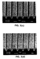
- FIG. 1 presents a scanning electron microscope ("SEM") cross-section obtained from bath 1 with 24g/L copper. Void-free fill was obtained for 0.5 ⁇ wide, 2:1 aspect ratio trench. The waveshape used was a forward pulse with 1 ms on and 1 ms off (WF1). It was found that the waveshape was not significant for fill as long as the current density was low.
- an electroplating waveform having low current density is used during the initial phases of the trench and/or via filling stage of the process. At some time subsequent to such initial filling, the electroplating waveform transitions to a higher current density waveform to complete the electroplating process and reduce the total time required for the process.
- an initial low current density approach is necessary for gap fill if no-additive bath is used.
- initial low current is helpful to improve the contact to the seed layer, particularly when the seed layer is very thin.
- the drawback of low current is its long processing time.
- a plating recipe with multiple steps is preferred in which a low current plating waveform is used to fill the small feature and, possibly, to enhance the seed layer, and then a high current plating waveform is used to finish the process and to provide smooth surface for one or more subsequent CMP processes.
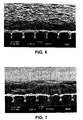
- Figure 5 shows a cross-section obtained with a two-step waveform of 4mA/cm 2 followed by 32mA/cm 2 . An improvement in gap fill was observed. Using the same two-step waveform, an increase in the copper concentration (36g/L) provided significant improvement of the fill process as illustrated in Figure 6 .
- FIG. 7 illustrates a metallization way are plated from such a bath using a 1-step waveform at 20 mA/cm 2 .
- Figure 8 is a cross-section obtained at 20mA/cm 2 with 20g/L copper in the solution. Although the surface of the deposit was smooth, similar to bath 3, voids were observed in the trench at this copper concentration. As the copper concentration decreased from 20 to 10g/L, void-free fill was obtained as in Figure 9 .
- the better gap fill at lower copper concentration in the presence of organic additives is different from that obtained for additive-free bath in which high copper provided better gap fill. This implies a different controlling mechanism for copper growth in the presence of additives. Similar to those obtained from additive-free bath, pulse reverse was found to produce voids and rough surface in this bath with additives.
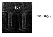
- Figures 10(a) - (c) illustrates the effect of seed layer on the gap fill.
- the center voids ( Figure 10a ) are formed when the top of the feature is pinched off before the filling is completed.
- the overhanging of the seed layer at the top of the feature due to the line-of-sight deposition inherent in the PVD process, is often the main reason for the center voids and the insufficient suppressor of copper growth at the top of the trench during the plating is the other one.
- the former needs the optimization of the PVD process to deposit a conformal layer and may possibly require a combination of PVD process and other techniques such as CVD or electrochemical deposition for small features.
- the latter calls for the optimization of the plating process by changing the bath composition and plating waveform.
- the bottom and sidewall voids are mainly attributed to the insufficient coverage of the seed layer. Copper oxide is always formed on the seed layer prior to the plating when the wafer is exposed to air. This oxide is readily removed, and the underlying copper can be chemically etched when the wafer is in contact with the acidic plating solution. This may lead to the exposure of the barrier layer to the solution and result in the formation of bottom or sidewall voids. There are ways to eliminate these voids either by having a thick layer in the feature or using less aggressive plating solutions for the copper plating. By optimizing the seed layer, void-free gap fill was achieved as in Fig. 10(c) .
Landscapes
- Chemical & Material Sciences (AREA)
- Organic Chemistry (AREA)
- Chemical Kinetics & Catalysis (AREA)
- Electrochemistry (AREA)
- Materials Engineering (AREA)
- Metallurgy (AREA)
- Engineering & Computer Science (AREA)
- Crystallography & Structural Chemistry (AREA)
- Electroplating Methods And Accessories (AREA)
- Electrodes Of Semiconductors (AREA)
- Battery Electrode And Active Subsutance (AREA)
- Secondary Cells (AREA)
- Electroplating And Plating Baths Therefor (AREA)
Claims (15)
- Verfahren zur Abscheidung eines Metalls in eine Mikrovertiefungen aufweisende Struktur in der Oberfläche eines mikroelektronischen Werkstücks, wobei das Verfahren aufweist:a) Herstellen eines Kontaktes zwischen der Oberfläche des Werkstücks und einer Lösung zur elektrochemischen Abscheidung in einer Zelle zur elektrochemischen Abscheidung, wobei die Zelle eine Anode aufweist, die in elektrischem Kontakt mit der Lösung angeordnet ist, und die Werkstückoberfläche eine Kathode bildet,b) in einer ersten Phase Abscheiden einer anfänglichen Schicht von Metall in die Mikrovertiefungen aufweisende Struktur unter Verwendung einer ersten Wellenform zur elektrochemischen Abscheidung mit einer ersten Stromdichte undc) in einer zweiten Phase im Wesentlichen Vervollständigen des Füllens der Mikrovertiefungen aufweisenden Struktur mit demselben Metall unter Verwendung einer zweiten Wellenform zur elektrochemischen Abscheidung mit einer zweiten, höheren Stromdichte.
- Verfahren nach Anspruch 1, bei dem die erste Phase für eine erste vorbestimmte Zeitdauer andauert und die zweite Phase nach Beendigung der ersten Zeitdauer anfängt.
- Verfahren nach einem der vorhergehenden Ansprüche, bei dem die Mikrovertiefungen aufweisende Struktur ein Halbleiterwafer ist.
- Verfahren nach einem der vorhergehenden Ansprüche, bei dem die Lösung zur elektrochemischen Abscheidung im Wesentlichen frei von organischen Zusatzstoffen ist und
eine erste vorbestimmte Konzentration des Metalls aufweist, das elektrochemisch abgeschieden werden soll, die höher als eine zweite vorbestimmte Konzentration ist, die zur Verwendung in einer Lösung zur elektrochemischen Abscheidung geeignet ist, die organische Zusatzstoffe enthält. - Verfahren nach Anspruch 4, bei dem die Lösung zur elektrochemischen Abscheidung eine Konzentration des Metalls aufweist, die zwischen ungefähr 15 g/L und 36 g/L beträgt.
- Verfahren nach einem der Ansprüche 1 bis 3, bei dem das Metall, das abgeschieden werden soll, Kupfer aufweist.
- Verfahren nach einem der Ansprüche 1 bis 3, bei dem das Verhältnis zwischen der ersten Stromdichte und der zweiten Stromdichte ungefähr 1:10 beträgt.
- Verfahren nach einem der Ansprüche 1 bis 3, bei dem das Verhältnis zwischen der ersten Stromdichte und der zweiten Stromdichte ungefähr 1:8 beträgt.
- Verfahren nach einem der Ansprüche 1 bis 3, bei dem die erste vorbestimmte Zeitdauer in der Größenordnung von 30 Sekunden liegt.
- Verfahren nach einem der vorhergehenden Ansprüche, bei dem die erste Wellenform zur elektrochemischen Abscheidung eine gepulste Wellenform ist.
- Verfahren nach einem der vorhergehenden Ansprüche, bei dem die Mikrovertiefungen aufweisende Struktur eine Breite von ungefähr 0,5 µm hat.
- Verfahren nach einem der vorhergehenden Ansprüche, bei dem die Mikrovertiefungen aufweisende Struktur ein Geometrieverhältnis von 2:1 aufweist.
- Verfahren nach einem der vorhergehenden Ansprüche, bei dem die anfängliche Schicht von Metall, die unter Verwendung der ersten Wellenform zur elektrochemischen Abscheidung abgeschieden wird, eine erste Morphologie aufweist und das zweite Metall, das unter Verwendung der zweiten Wellenform zur elektrochemischen Abscheidung abgeschieden wird, eine zweite Morphologie aufweist, die anders als die erste Morphologie ist.
- Verfahren nach einem der vorhergehenden Ansprüche, das den Schritt aufweist, vor der Abscheidung der anfänglichen Schicht eine dünne Keimschicht auf dem mikroelektronischen Werkstück abzuscheiden, wobei die Abscheidung der anfänglichen Schicht die dünne Keimschicht verbessert.
- Verfahren nach einem der vorhergehenden Ansprüche, das nach der Bearbeitung der Mikrovertiefungen aufweisenden Struktur mit der zweiten Wellenform zur elektrochemischen Abscheidung den Schritt aufweist, die Mikrovertiefungen aufweisende Struktur unter Verwendung einer dritten Wellenform zur elektrochemischen Abscheidung zu bearbeiten, die einen Gegenstromimpuls aufweist, um Überfüllung zu entfernen.
Applications Claiming Priority (3)
| Application Number | Priority Date | Filing Date | Title |
|---|---|---|---|
| US10306198P | 1998-10-05 | 1998-10-05 | |
| US103061P | 1998-10-05 | ||
| PCT/US1999/023187 WO2000020662A1 (en) | 1998-10-05 | 1999-10-05 | Submicron metallization using electrochemical deposition |
Publications (3)
| Publication Number | Publication Date |
|---|---|
| EP1125007A1 EP1125007A1 (de) | 2001-08-22 |
| EP1125007A4 EP1125007A4 (de) | 2003-05-28 |
| EP1125007B1 true EP1125007B1 (de) | 2010-08-11 |
Family
ID=22293166
Family Applications (1)
| Application Number | Title | Priority Date | Filing Date |
|---|---|---|---|
| EP99954748A Expired - Lifetime EP1125007B1 (de) | 1998-10-05 | 1999-10-05 | Submikrone metallisierung unter verwendung elektrochemischer beschichtung |
Country Status (5)
| Country | Link |
|---|---|
| EP (1) | EP1125007B1 (de) |
| JP (1) | JP2002526663A (de) |
| AT (1) | ATE477353T1 (de) |
| DE (1) | DE69942669D1 (de) |
| WO (1) | WO2000020662A1 (de) |
Families Citing this family (8)
| Publication number | Priority date | Publication date | Assignee | Title |
|---|---|---|---|---|
| US7244677B2 (en) | 1998-02-04 | 2007-07-17 | Semitool. Inc. | Method for filling recessed micro-structures with metallization in the production of a microelectronic device |
| JP3641372B2 (ja) * | 1998-10-21 | 2005-04-20 | 株式会社荏原製作所 | 電解めっき方法及び電解めっき装置 |
| US6913680B1 (en) | 2000-05-02 | 2005-07-05 | Applied Materials, Inc. | Method of application of electrical biasing to enhance metal deposition |
| JP2002121699A (ja) * | 2000-05-25 | 2002-04-26 | Nippon Techno Kk | めっき浴の振動流動とパルス状めっき電流との組み合わせを用いた電気めっき方法 |
| JP5000941B2 (ja) * | 2006-07-27 | 2012-08-15 | ルネサスエレクトロニクス株式会社 | 半導体装置の製造方法 |
| JP5767154B2 (ja) * | 2012-04-13 | 2015-08-19 | ルネサスエレクトロニクス株式会社 | 半導体装置の製造方法 |
| JP5749302B2 (ja) * | 2013-08-20 | 2015-07-15 | 株式会社荏原製作所 | めっき方法 |
| JP6450560B2 (ja) * | 2014-10-24 | 2019-01-09 | 新日本無線株式会社 | 半導体装置およびその製造方法 |
Family Cites Families (13)
| Publication number | Priority date | Publication date | Assignee | Title |
|---|---|---|---|---|
| FR960114A (de) * | 1942-05-04 | 1950-04-13 | ||
| US3894918A (en) * | 1973-12-20 | 1975-07-15 | Western Electric Co | Methods of treating portions of articles |
| US4250004A (en) * | 1980-02-25 | 1981-02-10 | Olin Corporation | Process for the preparation of low overvoltage electrodes |
| US4514265A (en) * | 1984-07-05 | 1985-04-30 | Rca Corporation | Bonding pads for semiconductor devices |
| US4869971A (en) * | 1986-05-22 | 1989-09-26 | Nee Chin Cheng | Multilayer pulsed-current electrodeposition process |
| JPH03104230A (ja) * | 1989-09-19 | 1991-05-01 | Fujitsu Ltd | 半導体装置の製造方法 |
| JPH03208347A (ja) * | 1990-01-10 | 1991-09-11 | Mitsubishi Electric Corp | 突起電極形成方法 |
| JPH07336017A (ja) * | 1994-06-08 | 1995-12-22 | Hitachi Ltd | 電流反転電解法による薄膜回路製造方法ならびにそれを用いた薄膜回路基板、薄膜多層回路基板および電子回路装置 |
| US5605615A (en) * | 1994-12-05 | 1997-02-25 | Motorola, Inc. | Method and apparatus for plating metals |
| JP3561582B2 (ja) * | 1996-09-18 | 2004-09-02 | 沖電気工業株式会社 | 半導体装置の製造方法 |
| JPH1098268A (ja) * | 1996-09-24 | 1998-04-14 | Oki Electric Ind Co Ltd | 柱状導体のめっき方法及びそれにより得られる多層プリント配線板 |
| US5972192A (en) * | 1997-07-23 | 1999-10-26 | Advanced Micro Devices, Inc. | Pulse electroplating copper or copper alloys |
| JP3694594B2 (ja) * | 1998-09-03 | 2005-09-14 | 株式会社荏原製作所 | 微細孔および/または微細溝を有する基材の孔埋めめっき方法 |
-
1999
- 1999-10-05 DE DE69942669T patent/DE69942669D1/de not_active Expired - Lifetime
- 1999-10-05 WO PCT/US1999/023187 patent/WO2000020662A1/en not_active Ceased
- 1999-10-05 EP EP99954748A patent/EP1125007B1/de not_active Expired - Lifetime
- 1999-10-05 AT AT99954748T patent/ATE477353T1/de not_active IP Right Cessation
- 1999-10-05 JP JP2000574753A patent/JP2002526663A/ja active Pending
Also Published As
| Publication number | Publication date |
|---|---|
| WO2000020662A9 (en) | 2000-09-14 |
| ATE477353T1 (de) | 2010-08-15 |
| EP1125007A1 (de) | 2001-08-22 |
| JP2002526663A (ja) | 2002-08-20 |
| DE69942669D1 (de) | 2010-09-23 |
| EP1125007A4 (de) | 2003-05-28 |
| WO2000020662A1 (en) | 2000-04-13 |
Similar Documents
| Publication | Publication Date | Title |
|---|---|---|
| US7144805B2 (en) | Method of submicron metallization using electrochemical deposition of recesses including a first deposition at a first current density and a second deposition at an increased current density | |
| US6290833B1 (en) | Method for electrolytically depositing copper on a semiconductor workpiece | |
| US6632345B1 (en) | Apparatus and method for electrolytically depositing a metal on a workpiece | |
| US6368966B1 (en) | Metallization structures for microelectronic applications and process for forming the structures | |
| US8197662B1 (en) | Deposit morphology of electroplated copper | |
| US6432821B1 (en) | Method of copper electroplating | |
| US6946065B1 (en) | Process for electroplating metal into microscopic recessed features | |
| US6399479B1 (en) | Processes to improve electroplating fill | |
| US6440289B1 (en) | Method for improving seed layer electroplating for semiconductor | |
| WO2000020662A9 (en) | Submicron metallization using electrochemical deposition | |
| US20020092673A1 (en) | Tungsten encapsulated copper interconnections using electroplating | |
| US20030146102A1 (en) | Method for forming copper interconnects | |
| KR100363847B1 (ko) | 반도체 소자의 금속 배선 형성 방법 | |
| KR100472859B1 (ko) | 반도체 소자의 금속 배선 형성 방법 | |
| US20050250327A1 (en) | Copper plating of semiconductor devices using intermediate immersion step |
Legal Events
| Date | Code | Title | Description |
|---|---|---|---|
| PUAI | Public reference made under article 153(3) epc to a published international application that has entered the european phase |
Free format text: ORIGINAL CODE: 0009012 |
|
| 17P | Request for examination filed |
Effective date: 20010418 |
|
| AK | Designated contracting states |
Kind code of ref document: A1 Designated state(s): AT BE CH CY DE DK ES FI FR GB GR IE IT LI LU MC NL PT SE |
|
| A4 | Supplementary search report drawn up and despatched |
Effective date: 20030410 |
|
| RIC1 | Information provided on ipc code assigned before grant |
Ipc: 7H 01L 21/768 B Ipc: 7H 01L 21/288 B Ipc: 7H 05K 3/42 B Ipc: 7C 25D 5/18 B Ipc: 7C 25D 5/10 B Ipc: 7C 25D 5/02 A |
|
| 17Q | First examination report despatched |
Effective date: 20070904 |
|
| GRAP | Despatch of communication of intention to grant a patent |
Free format text: ORIGINAL CODE: EPIDOSNIGR1 |
|
| GRAS | Grant fee paid |
Free format text: ORIGINAL CODE: EPIDOSNIGR3 |
|
| GRAA | (expected) grant |
Free format text: ORIGINAL CODE: 0009210 |
|
| AK | Designated contracting states |
Kind code of ref document: B1 Designated state(s): AT BE CH CY DE DK ES FI FR GB GR IE IT LI LU MC NL PT SE |
|
| REG | Reference to a national code |
Ref country code: GB Ref legal event code: FG4D |
|
| REG | Reference to a national code |
Ref country code: CH Ref legal event code: EP |
|
| REG | Reference to a national code |
Ref country code: IE Ref legal event code: FG4D |
|
| REF | Corresponds to: |
Ref document number: 69942669 Country of ref document: DE Date of ref document: 20100923 Kind code of ref document: P |
|
| REG | Reference to a national code |
Ref country code: NL Ref legal event code: VDEP Effective date: 20100811 |
|
| PG25 | Lapsed in a contracting state [announced via postgrant information from national office to epo] |
Ref country code: NL Free format text: LAPSE BECAUSE OF FAILURE TO SUBMIT A TRANSLATION OF THE DESCRIPTION OR TO PAY THE FEE WITHIN THE PRESCRIBED TIME-LIMIT Effective date: 20100811 Ref country code: FI Free format text: LAPSE BECAUSE OF FAILURE TO SUBMIT A TRANSLATION OF THE DESCRIPTION OR TO PAY THE FEE WITHIN THE PRESCRIBED TIME-LIMIT Effective date: 20100811 Ref country code: AT Free format text: LAPSE BECAUSE OF FAILURE TO SUBMIT A TRANSLATION OF THE DESCRIPTION OR TO PAY THE FEE WITHIN THE PRESCRIBED TIME-LIMIT Effective date: 20100811 |
|
| PG25 | Lapsed in a contracting state [announced via postgrant information from national office to epo] |
Ref country code: PT Free format text: LAPSE BECAUSE OF FAILURE TO SUBMIT A TRANSLATION OF THE DESCRIPTION OR TO PAY THE FEE WITHIN THE PRESCRIBED TIME-LIMIT Effective date: 20101213 Ref country code: CY Free format text: LAPSE BECAUSE OF FAILURE TO SUBMIT A TRANSLATION OF THE DESCRIPTION OR TO PAY THE FEE WITHIN THE PRESCRIBED TIME-LIMIT Effective date: 20100811 |
|
| PG25 | Lapsed in a contracting state [announced via postgrant information from national office to epo] |
Ref country code: GR Free format text: LAPSE BECAUSE OF FAILURE TO SUBMIT A TRANSLATION OF THE DESCRIPTION OR TO PAY THE FEE WITHIN THE PRESCRIBED TIME-LIMIT Effective date: 20101112 Ref country code: SE Free format text: LAPSE BECAUSE OF FAILURE TO SUBMIT A TRANSLATION OF THE DESCRIPTION OR TO PAY THE FEE WITHIN THE PRESCRIBED TIME-LIMIT Effective date: 20100811 Ref country code: BE Free format text: LAPSE BECAUSE OF FAILURE TO SUBMIT A TRANSLATION OF THE DESCRIPTION OR TO PAY THE FEE WITHIN THE PRESCRIBED TIME-LIMIT Effective date: 20100811 |
|
| PG25 | Lapsed in a contracting state [announced via postgrant information from national office to epo] |
Ref country code: DK Free format text: LAPSE BECAUSE OF FAILURE TO SUBMIT A TRANSLATION OF THE DESCRIPTION OR TO PAY THE FEE WITHIN THE PRESCRIBED TIME-LIMIT Effective date: 20100811 |
|
| PG25 | Lapsed in a contracting state [announced via postgrant information from national office to epo] |
Ref country code: MC Free format text: LAPSE BECAUSE OF NON-PAYMENT OF DUE FEES Effective date: 20101031 |
|
| REG | Reference to a national code |
Ref country code: CH Ref legal event code: PL |
|
| PLBE | No opposition filed within time limit |
Free format text: ORIGINAL CODE: 0009261 |
|
| STAA | Information on the status of an ep patent application or granted ep patent |
Free format text: STATUS: NO OPPOSITION FILED WITHIN TIME LIMIT |
|
| PG25 | Lapsed in a contracting state [announced via postgrant information from national office to epo] |
Ref country code: ES Free format text: LAPSE BECAUSE OF FAILURE TO SUBMIT A TRANSLATION OF THE DESCRIPTION OR TO PAY THE FEE WITHIN THE PRESCRIBED TIME-LIMIT Effective date: 20101122 |
|
| 26N | No opposition filed |
Effective date: 20110512 |
|
| GBPC | Gb: european patent ceased through non-payment of renewal fee |
Effective date: 20101111 |
|
| PG25 | Lapsed in a contracting state [announced via postgrant information from national office to epo] |
Ref country code: LI Free format text: LAPSE BECAUSE OF NON-PAYMENT OF DUE FEES Effective date: 20101031 Ref country code: CH Free format text: LAPSE BECAUSE OF NON-PAYMENT OF DUE FEES Effective date: 20101031 |
|
| REG | Reference to a national code |
Ref country code: DE Ref legal event code: R097 Ref document number: 69942669 Country of ref document: DE Effective date: 20110512 |
|
| PG25 | Lapsed in a contracting state [announced via postgrant information from national office to epo] |
Ref country code: IE Free format text: LAPSE BECAUSE OF NON-PAYMENT OF DUE FEES Effective date: 20101005 |
|
| PG25 | Lapsed in a contracting state [announced via postgrant information from national office to epo] |
Ref country code: GB Free format text: LAPSE BECAUSE OF NON-PAYMENT OF DUE FEES Effective date: 20101111 |
|
| REG | Reference to a national code |
Ref country code: GB Ref legal event code: 732E Free format text: REGISTERED BETWEEN 20120802 AND 20120808 |
|
| REG | Reference to a national code |
Ref country code: DE Ref legal event code: R081 Ref document number: 69942669 Country of ref document: DE Owner name: APPLIED MATERIALS, INC. (N.D.GES.D. STAATES DE, US Free format text: FORMER OWNER: SEMITOOL, INC., KALISPELL, MONT., US Effective date: 20120801 Ref country code: DE Ref legal event code: R081 Ref document number: 69942669 Country of ref document: DE Owner name: APPLIED MATERIALS, INC. (N.D.GES.D. STAATES DE, US Free format text: FORMER OWNER: SEMITOOL, INC., KALISPELL, US Effective date: 20120801 |
|
| PG25 | Lapsed in a contracting state [announced via postgrant information from national office to epo] |
Ref country code: LU Free format text: LAPSE BECAUSE OF NON-PAYMENT OF DUE FEES Effective date: 20101005 |
|
| PGFP | Annual fee paid to national office [announced via postgrant information from national office to epo] |
Ref country code: BE Payment date: 20121031 Year of fee payment: 14 Ref country code: DE Payment date: 20121031 Year of fee payment: 14 |
|
| PGFP | Annual fee paid to national office [announced via postgrant information from national office to epo] |
Ref country code: IT Payment date: 20121017 Year of fee payment: 14 |
|
| PGFP | Annual fee paid to national office [announced via postgrant information from national office to epo] |
Ref country code: FR Payment date: 20130924 Year of fee payment: 15 |
|
| BERE | Be: lapsed |
Owner name: APPLIED MATERIALS, INC. Effective date: 20131031 |
|
| REG | Reference to a national code |
Ref country code: DE Ref legal event code: R119 Ref document number: 69942669 Country of ref document: DE Effective date: 20140501 |
|
| PG25 | Lapsed in a contracting state [announced via postgrant information from national office to epo] |
Ref country code: DE Free format text: LAPSE BECAUSE OF NON-PAYMENT OF DUE FEES Effective date: 20140501 Ref country code: IT Free format text: LAPSE BECAUSE OF NON-PAYMENT OF DUE FEES Effective date: 20131005 |
|
| PG25 | Lapsed in a contracting state [announced via postgrant information from national office to epo] |
Ref country code: BE Free format text: LAPSE BECAUSE OF FAILURE TO SUBMIT A TRANSLATION OF THE DESCRIPTION OR TO PAY THE FEE WITHIN THE PRESCRIBED TIME-LIMIT Effective date: 20131031 |
|
| REG | Reference to a national code |
Ref country code: FR Ref legal event code: ST Effective date: 20150630 |
|
| PG25 | Lapsed in a contracting state [announced via postgrant information from national office to epo] |
Ref country code: FR Free format text: LAPSE BECAUSE OF NON-PAYMENT OF DUE FEES Effective date: 20141031 |