EP1126046A2 - Fabrication de barrières par CVD utilisant des précurseurs nouveaux - Google Patents
Fabrication de barrières par CVD utilisant des précurseurs nouveaux Download PDFInfo
- Publication number
- EP1126046A2 EP1126046A2 EP01103524A EP01103524A EP1126046A2 EP 1126046 A2 EP1126046 A2 EP 1126046A2 EP 01103524 A EP01103524 A EP 01103524A EP 01103524 A EP01103524 A EP 01103524A EP 1126046 A2 EP1126046 A2 EP 1126046A2
- Authority
- EP
- European Patent Office
- Prior art keywords
- metal
- nitride
- film
- tantalum
- group
- Prior art date
- Legal status (The legal status is an assumption and is not a legal conclusion. Google has not performed a legal analysis and makes no representation as to the accuracy of the status listed.)
- Withdrawn
Links
Images

Classifications
-
- H—ELECTRICITY
- H10—SEMICONDUCTOR DEVICES; ELECTRIC SOLID-STATE DEVICES NOT OTHERWISE PROVIDED FOR
- H10W—GENERIC PACKAGES, INTERCONNECTIONS, CONNECTORS OR OTHER CONSTRUCTIONAL DETAILS OF DEVICES COVERED BY CLASS H10
- H10W20/00—Interconnections in chips, wafers or substrates
- H10W20/01—Manufacture or treatment
- H10W20/031—Manufacture or treatment of conductive parts of the interconnections
- H10W20/032—Manufacture or treatment of conductive parts of the interconnections of conductive barrier, adhesion or liner layers
- H10W20/033—Manufacture or treatment of conductive parts of the interconnections of conductive barrier, adhesion or liner layers in openings in dielectrics
-
- C—CHEMISTRY; METALLURGY
- C23—COATING METALLIC MATERIAL; COATING MATERIAL WITH METALLIC MATERIAL; CHEMICAL SURFACE TREATMENT; DIFFUSION TREATMENT OF METALLIC MATERIAL; COATING BY VACUUM EVAPORATION, BY SPUTTERING, BY ION IMPLANTATION OR BY CHEMICAL VAPOUR DEPOSITION, IN GENERAL; INHIBITING CORROSION OF METALLIC MATERIAL OR INCRUSTATION IN GENERAL
- C23C—COATING METALLIC MATERIAL; COATING MATERIAL WITH METALLIC MATERIAL; SURFACE TREATMENT OF METALLIC MATERIAL BY DIFFUSION INTO THE SURFACE, BY CHEMICAL CONVERSION OR SUBSTITUTION; COATING BY VACUUM EVAPORATION, BY SPUTTERING, BY ION IMPLANTATION OR BY CHEMICAL VAPOUR DEPOSITION, IN GENERAL
- C23C16/00—Chemical coating by decomposition of gaseous compounds, without leaving reaction products of surface material in the coating, i.e. chemical vapour deposition [CVD] processes
- C23C16/06—Chemical coating by decomposition of gaseous compounds, without leaving reaction products of surface material in the coating, i.e. chemical vapour deposition [CVD] processes characterised by the deposition of metallic material
- C23C16/18—Chemical coating by decomposition of gaseous compounds, without leaving reaction products of surface material in the coating, i.e. chemical vapour deposition [CVD] processes characterised by the deposition of metallic material from metallo-organic compounds
-
- C—CHEMISTRY; METALLURGY
- C23—COATING METALLIC MATERIAL; COATING MATERIAL WITH METALLIC MATERIAL; CHEMICAL SURFACE TREATMENT; DIFFUSION TREATMENT OF METALLIC MATERIAL; COATING BY VACUUM EVAPORATION, BY SPUTTERING, BY ION IMPLANTATION OR BY CHEMICAL VAPOUR DEPOSITION, IN GENERAL; INHIBITING CORROSION OF METALLIC MATERIAL OR INCRUSTATION IN GENERAL
- C23C—COATING METALLIC MATERIAL; COATING MATERIAL WITH METALLIC MATERIAL; SURFACE TREATMENT OF METALLIC MATERIAL BY DIFFUSION INTO THE SURFACE, BY CHEMICAL CONVERSION OR SUBSTITUTION; COATING BY VACUUM EVAPORATION, BY SPUTTERING, BY ION IMPLANTATION OR BY CHEMICAL VAPOUR DEPOSITION, IN GENERAL
- C23C16/00—Chemical coating by decomposition of gaseous compounds, without leaving reaction products of surface material in the coating, i.e. chemical vapour deposition [CVD] processes
- C23C16/22—Chemical coating by decomposition of gaseous compounds, without leaving reaction products of surface material in the coating, i.e. chemical vapour deposition [CVD] processes characterised by the deposition of inorganic material, other than metallic material
- C23C16/30—Deposition of compounds, mixtures or solid solutions, e.g. borides, carbides, nitrides
- C23C16/34—Nitrides
-
- C—CHEMISTRY; METALLURGY
- C23—COATING METALLIC MATERIAL; COATING MATERIAL WITH METALLIC MATERIAL; CHEMICAL SURFACE TREATMENT; DIFFUSION TREATMENT OF METALLIC MATERIAL; COATING BY VACUUM EVAPORATION, BY SPUTTERING, BY ION IMPLANTATION OR BY CHEMICAL VAPOUR DEPOSITION, IN GENERAL; INHIBITING CORROSION OF METALLIC MATERIAL OR INCRUSTATION IN GENERAL
- C23C—COATING METALLIC MATERIAL; COATING MATERIAL WITH METALLIC MATERIAL; SURFACE TREATMENT OF METALLIC MATERIAL BY DIFFUSION INTO THE SURFACE, BY CHEMICAL CONVERSION OR SUBSTITUTION; COATING BY VACUUM EVAPORATION, BY SPUTTERING, BY ION IMPLANTATION OR BY CHEMICAL VAPOUR DEPOSITION, IN GENERAL
- C23C16/00—Chemical coating by decomposition of gaseous compounds, without leaving reaction products of surface material in the coating, i.e. chemical vapour deposition [CVD] processes
- C23C16/44—Chemical coating by decomposition of gaseous compounds, without leaving reaction products of surface material in the coating, i.e. chemical vapour deposition [CVD] processes characterised by the method of coating
- C23C16/455—Chemical coating by decomposition of gaseous compounds, without leaving reaction products of surface material in the coating, i.e. chemical vapour deposition [CVD] processes characterised by the method of coating characterised by the method used for introducing gases into reaction chamber or for modifying gas flows in reaction chamber
- C23C16/45561—Gas plumbing upstream of the reaction chamber
-
- H—ELECTRICITY
- H10—SEMICONDUCTOR DEVICES; ELECTRIC SOLID-STATE DEVICES NOT OTHERWISE PROVIDED FOR
- H10P—GENERIC PROCESSES OR APPARATUS FOR THE MANUFACTURE OR TREATMENT OF DEVICES COVERED BY CLASS H10
- H10P14/00—Formation of materials, e.g. in the shape of layers or pillars
- H10P14/40—Formation of materials, e.g. in the shape of layers or pillars of conductive or resistive materials
- H10P14/418—Formation of materials, e.g. in the shape of layers or pillars of conductive or resistive materials the conductive layers comprising transition metals
-
- H—ELECTRICITY
- H10—SEMICONDUCTOR DEVICES; ELECTRIC SOLID-STATE DEVICES NOT OTHERWISE PROVIDED FOR
- H10W—GENERIC PACKAGES, INTERCONNECTIONS, CONNECTORS OR OTHER CONSTRUCTIONAL DETAILS OF DEVICES COVERED BY CLASS H10
- H10W20/00—Interconnections in chips, wafers or substrates
- H10W20/01—Manufacture or treatment
- H10W20/031—Manufacture or treatment of conductive parts of the interconnections
- H10W20/032—Manufacture or treatment of conductive parts of the interconnections of conductive barrier, adhesion or liner layers
- H10W20/047—Manufacture or treatment of conductive parts of the interconnections of conductive barrier, adhesion or liner layers by introducing additional elements therein
- H10W20/048—Manufacture or treatment of conductive parts of the interconnections of conductive barrier, adhesion or liner layers by introducing additional elements therein by using plasmas or gaseous environments, e.g. by nitriding
-
- H—ELECTRICITY
- H10—SEMICONDUCTOR DEVICES; ELECTRIC SOLID-STATE DEVICES NOT OTHERWISE PROVIDED FOR
- H10W—GENERIC PACKAGES, INTERCONNECTIONS, CONNECTORS OR OTHER CONSTRUCTIONAL DETAILS OF DEVICES COVERED BY CLASS H10
- H10W20/00—Interconnections in chips, wafers or substrates
- H10W20/01—Manufacture or treatment
- H10W20/031—Manufacture or treatment of conductive parts of the interconnections
- H10W20/032—Manufacture or treatment of conductive parts of the interconnections of conductive barrier, adhesion or liner layers
- H10W20/052—Manufacture or treatment of conductive parts of the interconnections of conductive barrier, adhesion or liner layers by treatments not introducing additional elements therein
- H10W20/0523—Manufacture or treatment of conductive parts of the interconnections of conductive barrier, adhesion or liner layers by treatments not introducing additional elements therein by irradiating with ultraviolet or particle radiation
Definitions
- the present invention relates to a metallization process for manufacturing semiconductor devices. More particularly, the invention relates to a method for depositing metal and metal nitride layers by chemical vapor deposition of a precursor.
- VLSI very large scale integration
- ULSI ultra large scale integration
- the multilevel interconnect features that lie at the heart of this technology require careful processing of high aspect ratio features, such as vias, lines, contacts, and other features. Reliable formation of these features is very important to the VLSI and ULSI success and to the continued effort to increase circuit density and quality of individual substrates and die.
- the widths of vias, contacts and other features, as well as the dielectric materials between them decrease to less than one micron dimensions, i.e ., 0.25 ⁇ m or less, whereas the thickness of the dielectric layers remains substantially constant, with the result that the aspect ratios for the features, i.e., their height divided by width, increases.
- Many traditional deposition processes have difficulty filling sub-micron structures where the aspect ratio exceed 4:1, and particularly where it exceeds 10:1. Therefore, there is a great amount of ongoing effort being directed at the formation of void-free films for sub-micron features having high aspect ratios.
- Conducting metals such as aluminum, copper, and tungsten, are used to fill sub-micron features on substrates during the manufacture of integrated circuits.
- aluminum and copper can diffuse into the structure of adjacent dielectric layers which may form a conductive path and cause device failure.
- tungsten suffers from less than desirable adhesion to adjacent metal and dielectric layers which may cause the formation of interlayer defects, such as delamination of the tungsten from the patterned substrate, diffusion and less than desirable adhesion may be prevented by depositing a liner layer and/or a barrier layer in a feature before depositing the conducting metal.
- the liner layer is preferably composed of a metal that provides good adhesion to the underlying material; and the barrier layer deposited on the liner layer is often a nitride or silicon nitride of that metal which helps protect the underlying material from interlayer diffusion and chemical reactions with subsequently deposited materials.
- a diffusion barrier layer may comprise a tantalum or niobium layer, a tantalum nitride or niobium nitride layer, a tantalum/tantalum nitride or niobium/niobium nitride stack or other combinations of diffusion barrier materials.
- Tantalum, niobium and the respective nitride films have typically been deposited by physical vapor deposition (PVD) and by chemical vapor deposition (CVD) techniques at near atmospheric pressures.
- PVD physical vapor deposition
- CVD chemical vapor deposition
- MOCVD metal organic chemical vapor deposition
- atmospheric film deposition tends to deposit material on the surfaces of the chamber, which may subsequently flake or delaminate and become a particle problem within the chamber.
- Particle deposition in the chamber can produce layering defects in the deposited films and provide less than desirable interlayer adhesion.
- tantalum and niobium precursors there exists only a few commercially available tantalum and niobium precursors, and the precursors that are available produce films that have unacceptable levels of contaminants such as carbon and oxygen, thereby increasing the film's resistivity and producing films having low diffusion resistance, low thermal stability, and other undesirable film characteristics. Additionally, many precursors, such as for tantalum films, produce nitride films of less than desirable quality and a more effective metal nitride precursor is needed.
- the available nitride precursors often produce films that are highly resistive and, in some cases, may be insulative, typically as a result of the inability to control crystalline structure or the chemical structure of the film deposited from the precursor.
- metal films such as tantalum
- the film becomes increasingly resistive, and in the case of a tantalum nitride film, a high nitrogen content will eventually transition a good conducting phase with superior barrier properties, such as Ta 2 N, to a Ta 3 N 5 insulating phase.
- many of the available tantalum nitride precursors readily deposit an insulating Ta 3 N 5 phase.
- MOCVD techniques and precursors for depositing materials, such as silicon which can be added to the liner/barrier materials to improve diffusion resistance, chemical resistance, thermal stability or enhance interlayer adhesion.
- the invention generally provides for an organometallic precursor and a method of forming a metal and/or metal nitride on a substrate using the chemical vapor deposition of the organometallic precursor at sub-atmospheric pressures below about 20 Torr.
- One aspect of the invention provides a thermally decomposable organometallic precursor having the formula: (Cp(R) n ) x MH y-x wherein:
- an organometallic precursor of the formula (Cp(R) n ) x MH y-x is used process a substrate by depositing a metal or metal nitride film at sub-atmospheric pressures.
- the method comprises introducing the organometallic precursor into a processing chamber maintained at a pressure of less than about 20 Torr, exposing the organometallic precursor to a processing gas, and decomposing the organometallic precursor to deposit a film.
- the organometallic precursor may be deposited by a thermal or plasma-enhanced process.
- the method further comprises exposing the film to a plasma to remove contaminants, densify the film, and reduce the film's resistivity.
- a metal film comprising tantalum is deposited in a processing gas comprising argon, hydrogen, and combinations thereof, and is treated with a the plasma comprising argon, hydrogen, and combinations thereof.
- Another aspect of the invention provides a method of depositing a metal/metal nitride liner/barrier layer.
- the method comprises depositing a metal layer by either a thermal or plasma-enhanced decomposition of an organometallic precursor of the formula (Cp(R) n ) x MH y-x in the presence of a processing gas, such as argon or hydrogen, and the metal nitride layer is deposited on the metal layer by the decomposition of an organometallic precursor of the formula (Cp(R) n ) x MH y-x in a nitrating reactant gas ,such as nitrogen or ammonia (NH 3 ).
- a processing gas such as argon or hydrogen
- the same organometallic precursors may be used for the deposition of both the metal and metal nitride layers which may further occur sequentially in the same processing chamber.
- the organometallic precursor may deposit a metal silicide or metal silicon nitride film by the addition of a silicon containing reactant gas, such as silane, to the processing or reactant gases when decomposing the precursor.
- a silicon containing reactant gas such as silane
- the metal layer (and metal silicide layer) of the liner/barrier layer scheme is preferably exposed to a non-nitrating plasma and the metal nitride layer (and metal silicon nitride layer) may be exposed to either a nitrating or non-nitrating plasma following deposition.
- metal carbon nitride films may be deposited by foregoing the post deposition plasma treatment.
- a feature is formed on a substrate by depositing a dielectric layer on the substrate, etching a pattern into the substrate, depositing a metal layer on the substrate by the decomposition of an organometallic precursor of the formula (Cp(R) n ) x MH y-x in the presence of a processing gas, depositing a metal nitride layer on the substrate by the decomposition of an organometallic precursor of the formula (Cp(R) n ) x MH y-x in the presence of a nitrating reactant gas, and depositing a conductive metal layer on the metal nitride layer.
- the metal layer is preferably exposed to a non-nitrating plasma and metal nitride layer may be exposed to either a nitrating or non-nitrating plasma following the formation of the metal nitride layer on the metal layer.
- the conductive metal is preferably copper and may be deposited by physical vapor deposition, chemical vapor deposition, or electrochemical deposition, preferably electroplating or electroless deposition.
- the invention generally provides an organometallic precursor and a method of processing a substrate at sub-atmospheric pressures below about 20 Torr by forming a metal or metal nitride liner/barrier layer in a metallization stack on the substrate by chemical vapor deposition (CVD) of the organometallic precursor.
- the organometallic precursor has the formula (Cp(R) n ) x MH y-x is provided for the deposition of a metal or metal nitride film.
- the metal or metal nitride film is deposited on a heated substrate by thermal or plasma enhanced decomposition of the organometallic precursor having the formula (Cp(R) n ) x MH y-x in the presence of a processing gas.
- the processing gas may be an inert gas, such as helium and argon, and/or a reactant gas selected from the group of hydrogen, nitrogen, ammonia, silane, and combinations thereof, where the composition of the processing gas may deposit metal, metal nitride, metal carbon nitride, and metal silicon nitride films.
- a plasma comprises the processing gases and an inert gas such as argon.
- the metal and metal nitride films may be deposited from the same precursor sequentially in the same chamber, and may be used as a liner/barrier scheme in a conducting metal, preferably copper, metallization..
- the organometallic precursor may decompose by heating the substrate to a temperature above the decomposition temperature of the organometallic precursor between about 100°C and about 450°C, and preferably between about 250°C and about 450°C.
- the organometallic precursor may decompose by striking a plasma at a power between about 200 - and about 1000 Watts, more preferably, about 750 Watts. Once deposited, the metal or metal nitride film may then be exposed to a plasma to remove contaminants and reduce film resistivity.
- M represents the metal to be deposited, preferably a metal.
- Metals which can be deposited according to this invention are hafnium and the Group VB metals of vanadium, tantalum, and niobium.
- Y is the valence of the metal M of the precursor, with a valence of 4 for hafnium, and a valence of 5 for the Group VB metals.
- Cp is a cyclopentadienyl ring having the general formula (C 5 H 5 -) and forms a ligand with the metal, M.
- cyclopentadienyl groups Preferably between 1 and 4 cyclopentadienyl groups are used to form the precursor, and most preferably, the precursor contains two cyclopentadienyl groups.
- x is the number of cyclopentadienyl groups forming ligands with the metal M.
- R is a substituent group replacing one or more hydrogens on the cyclopentadienyl ring and n is the number of substituent groups disposed on the ring.
- the substituent group R is organic group, preferably having at least one carbon-silicon bond, and which may additionally contain at least one silicon-oxygen bond.
- the number of substituent groups on the cyclopentadienyl ring, represented by n, can number up to 5 when forming a ligand with the metal of the precursor.
- Silane and silioxane derived functional groups are exemplary organic compounds having at least one carbon-silicon bond which can be substituted on the cyclopentadienyl rings of the precursor.
- Preferred hydrocarbon substituents are alkylsilyl groups, preferably having from 1 to 3 hydrocarbyl substituent groups, where hydrocarbyl substituent groups are defined as carbon containing organic functional groups, for example, methyl and ethyl.
- the most preferred alkylsilyl groups are silyl (SiH 3 -), methylsilyl (CH 3 -SiH 2 -), dimethylsilyl ((CH 3 ) 2 -SiH-), trimethylsilyl ((CH 3 ) 3 -Si-), and combinations thereof.
- the substituent group may further include alkyl or alkenyl substituents on the same cyclopentadienyl ring with the silicon containing substituents to provide higher volatility.
- Other suitable substituents of the cyclopentadienyl ring include the fluorinated derivatives of the alkyl, alkenyl, or silicon containing substituents.
- a film can be deposited containing silicon, but preferably, a silicon containing processing gas such as silane is used to ensure sufficient silicon to form metal silicide and metal silicon nitride films.
- the presence of the substituent groups on the cyclopentadienyl groups, particularly the silicon containing substituent groups, provide for enhancing preferred physical properties such as increasing the precursor's volatility, decreasing the decomposition temperatures, and lowering the boiling points to the organometallic precursor than unsubstituted cyclopentadienyl functional groups.
- Preferred precursors have compositions that contain functional groups which allow the formation of heat decomposable organometallic compounds that are thermally stable at temperatures below about 150°C, but thermally decompose with the deposition of metal at a temperature from about 150°C to about 1000°C.
- Preferred precursors are also liquids at 100°C or below for efficient handling in current precursor liquid delivery systems for chemical vapor deposition chambers.
- Relatively low thermal decomposition temperatures of the precursors allow for economical operation of processing chambers at temperatures from about 150°C to about 1000°C, but preferably between about 100°C to about 450°C, and most preferably between about 250°C to about 450°C, with few, if any, requirements for special high temperature resistant equipment.
- the presence of substituent groups on the cyclopentadienyl rings also allows a greater temperature difference between the melting point and the decomposition temperature of the precursor in comparison to unsubstituted cyclopentadienyl rings.
- a large temperature difference between the melting point and decomposition temperature of the precursors allow the vaporization of the liquid precursors into a carrier gas stream at convenient operating temperatures of the liquid delivery system, preferably from about 60°C to about 100°C, without the risk of premature decomposition.
- the precursors preferably have high vapor pressures of at least 0.1 Torr at 100°C so as to ensure sufficient entrainment of the precursor in vaporized fluid flow to the processing chamber.
- the high volatility of the precursor compounds ensures a sufficiently high concentration of precursor in carrier gas for effective deposition of a metal containing film. Higher volatility will allow the use of vaporization of the precursor by sublimation and delivery to a processing chamber without risk of premature decomposition. Additionally, the presence of substituent cyclopentadienyl groups also provide sufficient solubility of the precursor for use in liquid delivery systems and in direct liquid injection systems.
- a metal, metal nitride, metal carbon nitride, and a metal silicon nitride film may be deposited.
- the film composition is determined by controlling the process gas composition and the plasma gas composition for the deposition process.
- a metal film is deposited in the presence of the processing gas, preferably non-nitrating reactant gases including hydrogen, silane, silane derivatives, and combinations thereof.
- the metal film is deposited in the presence of argon, hydrogen, and combinations thereof, but most preferably argon.
- Metal nitride films are deposited'in the presence of a nitrating reactant gas, preferred nitrating gases are selected from nitrogen, ammonia, and nitrogen and hydrogen combination gases.
- Silane and silane derivatives in combination with nitrating gases may also be used to deposit metal nitride films.
- Film deposited in the presence of a silane or silance derivative processing gas produce metal silicides and metal silicon nitrides.
- Metal carbon nitride films may be deposited by incomplete decomposition of the metal precursor, without a post deposition treatment plasma.
- the preferred metals for deposition are metal including hafnium, and the Group VB metals which include vanadium, tantalum, and niobium.
- the metal nitrides being nitrides, carbon nitrides, and silicon nitrides of the respective metals.
- a plasma treatment is used to lower the film's resistivity, remove contaminants, and densify the film to enhance barrier and liner properties.
- the plasma gas composition is preferably the processing gases used to deposit the film .
- Plasma treatment with nitrating gases may further nitrate a deposited film, which may be undesirable for nitrogen sensitive films, such as tantalum nitride, where non-nitrating plasma treatments are used.
- a plasma of argon, hydrogen, and combinations thereof, but most preferably argon is used in the post deposition plasma process.
- plasma treatments are not performed since the plasma treatment may remove the desired carbon content of the film.
- the plasma gases preferably comprise inert gases, such as argon and helium.
- the deposition and plasma treatment of the deposited film may be performed in the same or different chambers.
- the properties and stoichiometry of the films are also affected by the post-deposition plasma treatment.
- the plasma composition can also affect the nitrogen content of the deposited film by further adding nitrogen to the film and changing the metal nitride film's phase.
- the phase of the metal nitrides can also be controlled.
- Plasmas that do not nitrate the film are preferably used for films that are sensitive to nitrogen content, such as tantalum nitride, to minimize the film's resistivity and prevent formation of high nitrogen content insulative phases such as Ta 3 N 5 .
- a plasma composed of hydrogen and an inert gas may be used for tantalum nitride.
- Nitrating plasmas are preferably used on films where added nitrogen in the films does not have detrimental consequences to the film's properties, such as in niobium nitride films. Unlike tantalum, niobium nitride films of different stoichiometries are conducting films, so nitrogen content has a less effect on the films properties.
- Nitrating plasma gases are preferably ammonia and/or nitrogen and may include other gases such as hydrogen. Nitrating plasmas can further nitrate films to provide a preferred metal nitride grain growth that reduces sheet resistivity of the film and increases film densification.
- the film and post treating the deposited film will produce a film with improved material properties.
- the plasma process will remove resistive constituents, such as contaminants of carbon and oxygen, from the film to lower the films resistivity and improve electrical conductivity.
- the plasma process will also densify the film and remove layering defects, thereby improving the deposited film's diffusion resistance.
- the post deposition plasma will densify material disposed at the bottom of substrate features in preference over material disposed on the sidewalls of the feature. This forms a more conductive film at the bottom of the feature, at the contact point between different levels of the device, than on the sidewalls where the feature typically contacts insulator materials.
- the invention may be used to advantage in an liner/barrier deposition process to form a metal/metal nitride barrier/liner stack for a conductive metal layer.
- a metal layer is conformally deposited by a chemical vapor deposition (CVD) technique from the heat degradation of an organometallic precursor having the formula according to the invention in the presence of a processing gas.
- a metal nitride of the metal may then deposited by CVD technique from the decomposition of an organometallic precursor having the formula according to the invention in the presence of a nitrating reactant gas on the metal layer.
- the metal/metal nitride barrier/liner stack is deposited from the same precursor in the same processing chamber. Further, each deposited layer can be exposed to a post-deposition plasma prior to subsequent material depositions to enhance the effectiveness of the barrier/liner scheme by removing impurities and densifying the film.
- the plasma may use nitrating or non-nitrating gases, but preferably non-nitrating gases are used for metal films and nitrogen content sensitive metal nitride films, such as tantalum nitride.
- The-conductive metal deposited is preferably copper and may be deposited by physical vapor deposition, chemical vapor deposition, or electrochemical deposition, preferably by an electroplating or electroless deposition process.
- tantalum and/or tantalum nitride liner and barrier scheme While other metals, preferably vanadium, niobium, and hafnium, may be used with this process, the invention will be detailed below with reference to a tantalum and/or tantalum nitride liner and barrier scheme. Material differences between tantalum and other metals will be noted as necessary in the detailed description.
- the process deposits a metal or metal nitride layer, e.g., a liner/barrier layer, on a substrate in a processing chamber.
- the substrate used for the decomposition process can be of any material, usually either metallic or ceramic, on which an adherent metallic film can be formed and which can be heated to a temperature above the decomposition temperatures of the precursor compounds.
- the substrate can be a ceramic material such as glass, thermal oxides, or quartz, or a metal such as iron, nickel, titanium, tungsten, copper, or aluminum.
- the substrate must be a solid at the decomposition temperature of the precursor.
- the substrate may also comprise patterned wafers including those having dielectric layers such as silicon and metal layers such as aluminum and can include a series of underlying layers and interconnects of various materials.
- patterned wafers including those having dielectric layers such as silicon and metal layers such as aluminum and can include a series of underlying layers and interconnects of various materials.
- Figure 1 is a schematic cross-sectional view of an exemplary metallized film stack 100 of the invention having a liner layer 118, a barrier layer 119, and conducting metal layer 120 deposited in a feature 116 formed on a substrate 112.
- the feature 116 is formed by depositing and etching a dielectric layer 114 on the substrate 112 to form the desired aspect of the feature 116, such as a via, contact, trench, or line.
- the dielectric layer 114 can be a pre-metal dielectric layer deposited over a silicon wafer or an inter-level dielectric layer, and is formed over the underlying substrate 112 in accordance with procedures conventionally known in the art to form a part of the overall integrated circuit. Once the dielectric layer 114 is deposited, the dielectric layer 114 can be etched with any dielectric etching or patterning process known in the art, preferably reactive ion etching techniques.
- the liner layer 118 of the invention is deposited from the organometallic precursor conformally on the dielectric layer 114 and on the floor and walls of the feature 116.
- the liner layer 118 improves adhesion between the substrate or dielectric layer 114 and the subsequently deposited conducting metal layer 120.
- the liner layer 118 is preferably deposited by either thermal decomposition or plasma enhanced decomposition of a tantalum precursor in the presence of a processing gas to form a metal layer.
- the deposition rate is preferably from about 30 angstroms ( ⁇ ) to about 50 ⁇ per minute, with a total layer thickness preferably from about 50 ⁇ to about 100 ⁇ thick.
- Thermal decomposition of the precursor involves heating the substrate to a temperature sufficiently high to cause the hydrocarbon portion of the volatile metal compound adjacent the substrate to decompose to volatilize hydrocarbons which desorb from the substrate while leaving the metal on the substrate.
- a reactant gas allows a greater deposition rate and the decomposition of the precursor is accelerated by the presence of reactant species.
- the exact temperature will depend upon the identity and chemical, thermal, and stability makeup of the organometallic precursor and processing gases used under the deposition conditions. However, a temperature from about room temperature to about 1000°C is contemplated for the thermal decomposition of the precursor of the invention.
- the substrate is heated to a temperature between about 100°C to about 450°C, preferably between about 250°C to about 450°C, and most preferably a temperature of 400°C is used to ensure a complete reaction between the precursor and the reacting gas on the substrate surface.
- the precursor For plasma-enhanced CVD deposition of the precursor, power to generate a plasma is then either capacitively or inductively coupled into the chamber to excite the plasma gases into excited neutral ions and the like which result in a deposit film on the substrate.
- the power is provided to the processing gases at about 200 to about 1000 Watts, with about 750 Watts most preferably used.
- the chamber pressure is maintained between about 100 milliTorr and about 20 Torr during the plasma enhanced deposition process.
- the plasma enhanced decomposition of the precursor allows for an increased deposition rate, particularly in combination with a reactant gas, at a lower substrate temperature as the energy to enable decomposition of the precursor is supplied externally by a power supply.
- the temperature of the substrate is preferably between about 100°C to about 450°C, and most preferably between about 250°C to about 450°C.
- the organometallic precursor for a tantalum film is introduced into the chamber at a flow rate of between about 5 and about 50 sccm, while the processing chamber is preferably maintained at a pressure between about 100 milliTorr to about 250 milliTorr, and more preferably at about 150 milliTorr. If the precursor cannot be delivered to the chamber as a gas, the precursor can be dissolved in a solvent and vaporized for delivery to the chamber. Aliphatic hydrocarbon based solvents such as hexane and octane are preferably used when the precursor are delivered to the processing chamber by a liquid delivery system.
- a molar ratio of 1:1 of precursor and solvent is preferably used, however, the molar ratio may vary according to the processing condition of the deposition process and the composition of the precursor.
- the flow rates to the chamber are between about 5 and about 50 sccm, and the chamber pressure for deposition is preferably from about 100 milliTorr to about 1 Torr.
- Processing gases are introduced into the chamber at a flow rate of between about 5 and about 50 sccm, with the flow rate is preferably being maintained to produce a molar ratio of 1:1 of precursor and reactant gas, however, the molar ratio may vary according to the processing condition of the deposition process and the composition of the precursor.
- the processing gases preferably comprise non-nitrating gases such as argon, hydrogen and combinations thereof.
- the metal film can be deposited in the presence of a non-reactant gas, such as argon.
- Non-conducting contaminants, such as carbon and oxygen impurities, in the deposited tantalum liner layer 118 may produce a film with high film resistivities and poor barrier properties. Therefore, a post-deposition plasma treatment is preferably performed to remove impurities, densify the film, and decrease the liner layer's resistivity.
- the plasma may have the same composition as the processing gas during deposition.
- a non-nitrating plasma gas is used, preferably of the same composition as the processing gas and any inert gases in the chamber.
- the plasma gas is argon, hydrogen, and combinations thereof.
- an argon plasma is used, preferably subsequent to depositing a metal film in an argon gas.
- the preferred carrier gas of the vaporized tantalum precursor is argon. Hydrogen species in the plasma react with the carbon impurities to produce volatile hydrocarbons that can easily desorb from the substrate surface and can be purged from the processing zone and processing chamber. The plasma further bombards the oxygen contained in the film to break oxygen bonds and produce oxygen radicals which also desorb from the film. By using an in situ plasma of the same composition as the reactant and carrier gases, no new production steps are required for the metallization process and a higher substrate throughput is achieved.
- the chamber pressure for the plasma treatment of the film is between about 50 milliTorr to about 10 Torr.
- the substrate temperature during the plasma step is preferably about the same temperature range as for the precursor decomposition temperature range, preferably from about 100°C to about 450°C, and most preferably 250°C to about 450°C.
- Power to generate a plasma is then either capacitively or inductively coupled into the chamber to excite the plasma gases into excited neutrals and the like which react with the deposited film on the substrate.
- the power is provided to the processing gases at about 200 to about 1000 Watts, with about 750 Watts most preferably used.
- the barrier layer 119 preferably composed of a tantalum nitride (Ta x N y , wherein x and y are integers representing the different phases of tantalum nitride films, such as TaN and Ta 3 N 5 ) film conformally deposited by the thermal decomposition of a (Cp(R) n ) x MH y-x precursor of the invention, such as ((Si(CH 3 ) 3 )C 5 H 4 ) 2 TaH 3 in the presence of a reactant gas, such as hydrogen, on the liner layer 118.
- the tantalum nitride barrier layer 119 may comprise a tantalum carbon nitride or tantalum silicon nitride film.
- the barrier layer 119 is deposited prior to the conducting metal layer 120 to prevent diffusion from the conducting metal layer 120 to the underlying substrate 112 or dielectric layer 114.
- the barrier layer 119 is preferably deposited by decomposition of a tantalum precursor of the invention, such as ((Si(CH 3 ) 3 )C 5 H 4 ) 2 TaH 3 in the presence of a nitrating reactant gas, such as ammonia, to form a tantalum nitride barrier layer 119.
- a nitrating reactant gas such as ammonia
- the same precursor is used for the deposition of both the metal and metal nitride layers.
- the nitrating reactant gas are preferably nitrogen, ammonia, nitrogen and hydrogen, and combinations thereof, most preferably ammonia.
- the same precursor deposited with different processing gas compositions allows for metal and metal nitride depositions to occur in the same chamber under similar processing conditions resulting in faster substrate throughput and minimal contamination.
- the organometallic precursor for a tantalum nitride film is introduced into the chamber at a flow rate of between about 5 and about 50 sccm.
- the processing chamber pressure is maintained at a pressure between about 100 milliTorr to about 10 Torr, preferably about 100 milliTorr to about 250 milliTorr, and most preferably about 150 milliTorr. If the precursor cannot be delivered to the chamber as a gas, the precursor can be dissolved in a solvent, such as hexane, and vaporized for delivery to the chamber.
- a molar ratio of 1:1 of precursor and solvent is preferably used, however, the molar ratio may vary according to the processing condition of the deposition process and the composition of the precursor.
- the flow rates to the chamber are similar, but the chamber pressure would preferably be from about 100 milliTorr to about 1 Torr.
- the nitrating reactant gases such as nitrogen and ammonia are introduced into the chamber at a flow rate of between about 5 and about 100 sccm.
- a molar ratio of 1:1 of precursor and nitrating reactant gas is preferably used, however, the molar ratio may vary according to the processing condition of the deposition process and the composition of the precursor.
- Non-reactant gases such as the inert gases argon and helium, can also be present in the processing chamber during deposition.
- a metal nitride film may be improved by incorporating silicon into the film to form a metal silicon nitride film.
- Silane can be used as a reactant gas in conjunction with nitrating reactant gases can deposit a metal silicon nitride layer, including tantalum silicon nitride (TaSiN) and niobium silicon nitride (NbSiN). Since the composition of the reactant gas determines the amount of nitrogen included in the deposited film, control of the composition and amount of reactant gases can produce nitrogen free metal films or particular phases of metal nitride and metal silicon nitride films.
- TaSiN tantalum silicon nitride
- NbSiN niobium silicon nitride
- the reactant gas composition for the metal nitride layer determines the film's characteristics and properties.
- the nitrogen content of the reactant can be controlled to determine the amount of nitration in the deposited film.
- inert gases such as the carrier gases argon and helium, are used to tune the conditions by selecting precursors that favor more or less nitrogen as desired.
- the tantalum nitride barrier layer 119 may be further exposed to a plasma to remove contaminants, densify the film, and reduce the resistivity of the film.
- the plasma reduces the barrier layer's 119 conductive resistivity by the removal of non-conducting contaminants, such as carbon and oxygen, from the deposited film as carbon reacts with hydrogen and is removed as volatile hydrocarbons and oxygen is displaced and desorbed from the film by nitrogen or hydrogen. Removal of the contaminants will also provide for a denser film with fewer layering defects and improved barrier properties.
- a plasma gas of the same composition as the reactant and carrier gases is used so no new processing steps are performed and a higher substrate throughput can be achieved.
- a hydrogen or hydrogen and argon plasma is preferably used for nitrogen sensitive films, such as the tantalum nitride layer 119.
- the plasma is performed at a processing chamber pressure of about 50 milliTorr to about 10 Torr with the plasma power is provided to the plasma gases at about 200 to about 1000 Watts, with about 750 Watts most preferably used.
- the effectiveness of the plasma treatment depends on the thickness of the untreated film and plasma conditions. With a fixed plasma power and treatment time, the thinner the deposited film, the more effective the treatment.
- the post-deposition plasma treatment has the further benefit of reducing temperature variations during sequential substrate depositions thereby eliminating the first wafer effect and maintaining a more stable processing regime.
- a conducting metal layer 120 preferably copper is deposited on the barrier layer 119 to fill the interconnect structure 116and simultaneously cover the entire field region between adjacent features such as interconnect 116 with copper.
- the conducting metal layer 120 may comprise a seed layer of a conducting metal for a subsequent deposition of a metal layer by a electroplating or electroless process.
- the seed layer allows for a conducting metal, such as copper, to fill the feature 116 formed in the substrate without forming voids or other deposition discontinuities.
- the barrier layer 119 functions as an seed layer for deposition of the conducting metal layer by an electroplating process to reduce processing steps for the metallization scheme.
- the copper layer 120 can be deposited by physical vapor deposition (PVD), ionized metal plasma (IMP) PVD, CVD, electroplating, electroless deposition, evaporation, or any other known methods in the art, but the copper layer 120 is preferably deposited by electroplating techniques.
- the feature 116 may be further processed by planarizing the top portion of the metallized film stack 100, preferably by chemical mechanical polishing (CMP). During the planarization process, portions of the copper layer 118 and the dielectric layer 114 are removed from the top of the structure leaving a fully planar surface with exposed upper surfaces of conductive features such as the via 116 therein.
- CMP chemical mechanical polishing
- the organometallic precursor is introduced into the processing chamber by either a liquid delivery system or a precursor vaporizer system.
- the organometallic precursor of the invention may be a liquid or a solid. In a liquid state, the precursor is delivered to the processing chamber by a liquid delivery system, and in a solid state, the precursor is delivered to the processing chamber by a precursor vaporizer system, where the vaporizer provides heat to vaporize or sublime the precursor.
- precursors with high viscosities may be first dissolved in an aliphatic hydrocarbon solvent, such as hexane or octane, to reduce the viscosity of the liquid precursor.
- the precursor is then stored in an ampoule or storage container in the system until a pressurized inert gas forces the precursor into a processing liquid path such as by supplying the inert gas under pressure into the ampoule containing the precursor.
- a flow meter regulates the liquid precursor flow and the flow rate can be varied from 1 mg/min to 1000 mg/min, or any other amount needed for the deposition process.
- the precursor liquid After flowing past the liquid flow meter, the precursor liquid is vaporized in a vaporizer and preferably injected into an inert carrier gas stream, such as helium or argon, for delivery to the processing chamber, preferably a CVD TXZTM chamber available from Applied Materials of Santa Clara, California.
- an inert carrier gas stream such as helium or argon
- the liquid delivery system vaporizer is often heated between about 50°C to about 120°C to facilitate the vaporization process.
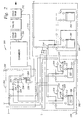
- FIG. 2 is a schematic view showing a liquid delivery system 200 of the invention.
- the liquid delivery system generally includes a liquid precursor module 202, a solvent module 204 and a vaporizer module 206.
- the liquid precursor module 202 includes two pressurized ampoules 208, 210 and a liquid delivery line 212 connected to each ampoule. Valves are disposed along the length of the liquid delivery lines to control flow of liquid from the ampoules to a mixing port and then into the vaporizer and to prevent collection of precursor within the system which can negatively affect process stabilization and/or repeatability.
- the ampoules are designed to deliver the liquid precursors at high pressure, e.g., up to 500 psi, without having to rely on high pressure pumps, i.e., no high cycle mechanical pump with rubbing parts exposed to precursors.
- an inert gas such as argon is charged into the ampoules at a pressure of about 90 psi through line 220.
- a liquid outlet line 222 is disposed in the ampoule so that as the inert gas, e.g., argon, is delivered to the ampoule and the appropriate valves are opened, the liquid is forced out through the outlet through a suitable valve and into the liquid delivery line.
- the delivery line 212 is connected from each ampoule to the vaporizer 254.
- a first valve is disposed on the outlet of the ampoule to control delivery of the liquid to the delivery line 212.
- the valve is preferably a three-way valve connecting the bypass line 218 and the liquid delivery line 212.
- the bypass line 218 in turn is connected to a second cold trap 252 and an exhaust manifold (not shown).
- a high pressure gauge 224 and a liquid flow controller (LFC) 226 are disposed downstream from a valve 228 introducing the solvent and the purge gas.
- the LFC controls delivery of the liquid to the mixing port 230 connected between the liquid precursor delivery lines.
- a low pressure gauge 232 is disposed on the bypass line 218 to monitor pressure in the line so that completion of the maintenance routine can be determined.
- the liquid precursor delivery lines 212 deliver liquid precursors into the mixing port 230 upstream from the vaporizer 254.
- a solvent delivery line 234 also delivers a solvent into the liquid delivery line downstream from the mixing port where the liquid precursors and the solvent are mixed and delivered into the vaporizer.
- a carrier gas line 236 delivers a carrier gas into the delivery line to carry the liquid precursors and the solvent into the vaporizer 254 through the capillary tube or nozzle.
- a concentric carrier gas line 238 delivers a carrier gas around the nozzle or injection tip to ensure that even a small amount of liquid is 'delivered to the vaporizing surfaces.
- the delivery line from the mixing port and into the vaporizer is preferably made of a material having a low coefficient of friction, such as Teflon PTFE, and does not hang up in the line. This feature assists in the delivery of small volumes of liquid precursor.
- the solvent module 204 includes one or more chargeable ampoules similar to the liquid precursor ampoules. Preferably, there are two solvent ampoules 240, 242 and two liquid precursor ampoules 208, 210.
- the liquid precursor ampoules can deliver two separate precursors which can be mixed at the mixing port or can deliver the same precursor together or alternatively.
- the liquid precursor ampoules are designed with a slotted/sculptured bottom to draw the liquid downwardly in the ampoule so that the liquid may (1) be detected at very low levels and (2) be drawn out of the ampoule even at low levels. This is particularly important in dealing with expensive liquids which are preferably not wasted.
- the ampoules include an ultrasonic detector for discerning the volume of liquid in the ampoule even at low levels so that continuous processing may be achieved.
- An optional cold trap 250 is disposed in the conduit connecting the exhaust pump to filter out the deposition material which may be detrimental to the pump. Additionally, a second cold trap 252 is disposed downstream from the first cold trap and is connected to a bypass line 218 from the vaporizer. The bypass line 218 and related cold trap 252 allow the system to operate in a continuous flow made by allowing delivery of vaporized material thereto during substrate transfer and plasma processing. By this method, the system may continually vaporize precursors but deliver the vaporized material to the processing chamber for deposition or to the exhaust system through a bypass line. The continual flow of the vaporized precursor enables stabilization of the deposition process over a number of substrates by providing consistent deposition processing conditions through optimization and maintenance of the vaporization process.
- Improved filtration of the deposition material may be accomplished by providing a cold trap 252 comprising a cold unit and a hot unit (not shown).
- the cold unit of the cold trap provides for removal of particulate material by condensation on the cold trap surface.
- the hot unit provides for removal of unreacted precursor vapor by having a temperature above the degradation temperature of the deposition precursor, thereby depositing the precursor material on the unit.
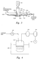
- Figure 3 shows a precursor vaporizer system, where a vaporizer 310 is provided to heat and vaporize or sublime the precursor.
- the vaporizer 310 generally comprises a metal cylinder of stainless steel or aluminum.
- a heated pressure gauge (not shown) is located in the vaporizer to monitor the pressure of the vaporizer to insure that a continuous feed of particulate solid or liquid precursor is provided to the vaporizer 310.
- the pressure gauge is preferably heated so that material will not deposit or decompose on the gauge and render the gauge inoperable.
- a vaporization chamber or vaporizer 310 is shown heating the starting material to vaporize or sublime a liquid or solid precursor material before introducing it into the deposition chamber or blending it with another precursor.
- a gas inlet port 316 permits the flow of a non-reactive gas into vaporizer 310.
- a gate valve 320 separates the vaporizer 310 from the processing chamber (not shown).
- the containment vessel 318 which may rest on the inner surface of the vaporizer 310, is made of a non-reactive material, usually a ceramic material, and preferably comprises quartz. Alternatively, an inert gas may be bubbled (not shown) provided to the containment vessels to enhance vaporization of the precursors of the invention.
- the pressure in vaporizer 310 may be maintained at atmospheric pressure, but for the chemical vapor deposition process, the pressure is preferably maintained from about 30 milliTorr to about 10 Torr, or any suitable pressure used by the CVD processing chamber for deposition of the precursor.
- the increase in total pressure up to 10 Torr increases the deposition rate of the precursor and allows better control of the amount of precursor that is provided to the deposition chamber.
- the carrier gas can be any inert gas, preferably helium or argon, and most preferably argon.
- the temperature of vaporizer 310 when operated within the previously described pressure ranges, will usually vary from a minimum temperature below which the material will not vaporize, at the pressure required for deposition, up to a maximum temperature below the temperature at which the vaporized material will decompose, at the operative pressure.
- the substituent groups on the precursor have a strong influence on the boiling point and decomposition temperature of the precursor, which provides for operating temperature that reflect the decomposition temperatures of the individual precursors. While the operating temperature of the vaporizer will vary according to the material to be vaporized, the temperature is preferably maintained between about 50°C and about 200°C.
- FIG. 4 An alternative embodiment for the vaporizer 310 is shown in Figure 4 wherein a thermostatic oven 306 heats the vaporizer 310 which contains, for example, non-vaporized and vaporized precursor.
- the carrier gas is passed through a flow controller 302 such as a metering pump or a needle valve and is bubbled through the non-vaporized precursor in the vaporizer 310.
- the combined carrier gas and vaporized precursor are then passed to the processing chamber by a rough pump 350.
- a mass flow meter (not shown) can be placed anywhere between the vaporizer 310 and the deposition chamber to measure the total mass leaving the vaporizer 310.
- the flow rate of precursor can then be calculated by subtracting the mass of carrier gas sent to the vaporizer 310 from the mass of material leaving the vaporizer 310.
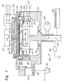
- FIG. 5 a schematic cross-sectional view of a suitable CVD plasma for performing the processes of the invention is shown.
- the methods of the invention are preferably carried out in a processing chamber that has been programmed to process a substrate accordingly.
- a preferred CVD chamber is known as the CVD TxZ chamber and is available commercially from Applied Materials, Inc., of Santa Clara, California.
- the CVD TxZ chamber is suitable for the deposition of an organometallic precursor of the invention in the presence of a reactant gas for depositing a metal and/or metal nitride layer by either the thermal or plasma enhanced decomposition process.
- a dual manifold distributor, or showerhead 440 provides for the introduction of the precursor and of the reactant gases to the processing zone.
- An exemplary dual manifold showerhead is shown in United States Patent Application No. 09/207,780, entitled “Dual Channel Gas Distribution Plate”, filed on December 9, 1998, which is assigned to common assignee and incorporated herein by reference.
- an organometallic precursor gas of the invention is injected into the chamber through the showerhead 440 at a preferable pressure from about 100 milliTorr to about 10 Torr while the pedestal 432 holds the substrate 436 at an elevated temperature above the decomposition temperature of the organometallic precursor of about 100°C to about 450°C, preferably from about 250°C to about 450°C.
- the reactant gas is introduced into the system through a second manifold in the shower head 440 to a volume located directly above the substrate for film deposition. Thereby, a metal and/or metal nitride layer is conformally deposited on the substrate 436 in a CVD process.
- the heat decomposition process is a thermal process not usually relying upon plasma excitation of the precursor gas. If a plasma is desired during the deposition process or as a post deposition plasma treatment to remove impurities and densify the film, sufficient voltage and power is applied by the RF source 494 to cause the process gas in the processing region 456 between the showerhead 440 and the pedestal 432 to discharge and to form a plasma.
- the CVD chamber 430 includes a pedestal 432 supporting a substrate 436 on a supporting surface 434 to be deposited by CVD with a layer of material, such as a TaN layer of the invention.
- Lift pins 438 are slidable within the pedestal 432 but are kept from falling out by conical heads on their upper ends. The lower ends of the lift pins 438 are engageable with vertically movable lifting ring 439 and thus can be lifted above the surface 434 of the pedestal 432.
- the surface 434 has a smaller diameter than that of the substrate 436 resting thereon.
- a robot blade (not shown) in cooperation with the lift pins 438 and the lifting ring 439 transfers the substrate 436 in and out of the chamber 430 through the slit valve 506, which can be vacuum-sealed to prevent the flow of gas into or out of the chamber through slit valve 506.
- Lift pins 438 raise an inserted substrate 436 off the robot blade and allowing the blade to retract from the chamber, and then the pedestal 432 rises to transfer the substrate 436 from the lift pins 438 onto the supporting surface 434 of the pedestal 432.
- a suitable robotics transfer assembly is described in commonly-assigned U.S. Patent No. 4,951,601, issued to Maydan , the complete disclosure of which is incorporated herein by reference.
- the process gas is injected into the reactor 430 through a central gas inlet 530 in a gas-feed cover plate 446 which houses a coaxially disposed gas delivery conduit 532.
- the conduit 532 channels a second gas into the processing region 454, which is received at a lower end of the conduit 532, and delivers a gas to the second gas pathway (not shown), which includes the second set of horizontal channels.
- the central bore 530 and the outer perimeter of the conduit 532 define a gas delivery passage 534, such as an annulus, which delivers a gas above the perforated blocker plate 452 to a first disk-shaped space or region 448 and from thence through passageways 450 in a baffle plate (or a gas blocker plate) 452 to a second disk-shaped space or region 454 in back of the showerhead 440.
- the showerhead 440 includes a large number of holes or passageways 442 for jetting the process gases into a processing region or zone 456. More specifically, process gas passes from the space or void 454, through the passageways 442 and into the processing space or zone 456 and towards the substrate 436.
- the process gas byproducts subsequently flow radially outwardly with respect to a central axis 500 across the edge of the substrate 436, and across a peripheral centering right 502 which is disposed in an annular ledge 504 recessed in the upper periphery of a pedestal 432.
- the pumping channel 460 is connected through a constricted exhaust aperture 462 to a pumping plenum 476, and a valve 478 gates the exhaust through an exhaust vent 480 to a vacuum pump 482.
- the restricted choke aperture 462 creates a nearly uniform pressure around the circumferential pumping channel 460.
- the process gas and its reaction byproducts flow from the center of the showerhead 440 across the substrate 436 and the periphery of the pedestal 432 and then through the choke aperture 462 to the pumping channel 460.
- the gas then flows circumferentially in the pumping channel 460 to the exhaust aperture 474 and then through the exhaust plenum 476 and the exhaust vent 480 to the vacuum pump 482. Because of the restriction 462 the gas flow across the substrate 436 is nearly uniform in the azimuthal direction.
- the ledge 470 in the chamber body 472 supports an insulating annular chamber insert 508 composed of a insulating chamber ring 510 and a band shield 512, which forms the bottom of the pumping channel 460.
- the chamber lid rim 466 forms the top and part of the outside wall of the pumping channel 460 along with the part of the chamber body 472.
- the inside upper edge of the pumping channel 460 is formed by the isolator ring 464, which is made of a ceramic or other electrically insulating material which insulates the metallic showerhead 40 from the chamber body 472.
- the CVD reactor 430 of Figure 5 can be operated in two modes, thermal and plasma-enhanced.
- an electrical power source 490 supplies power to a resistive heater 492 at the top of the pedestal 432 to thereby heat the pedestal 432 and thus the substrate 436 to an elevated temperature sufficient to thermally activate the CVD deposition reaction.
- an RF electrical source 494 is passed by a switch 496 to the metallic showerhead 440, which thus acts as an electrode.
- the showerhead 440 is electrically insulated from the lid rim 466 and the main chamber body 472 by the annular isolator ring 464, typically formed of an electrically non-conductive ceramic.
- the pedestal 432 is connected to a biasing element 498 associated with the RF source 494 so that RF power is split between the showerhead 440 and the pedestal 432. Sufficient voltage and power is applied by the RF source 494 to cause the process gas in the processing region 456 between the showerhead 440 and the pedestal 432 to discharge and to form a plasma.
- a microprocessor controller 499 is provided to monitor and control the deposition processes performed in the chamber 430.
- the generally illustrated chamber insert 508 includes an L-shaped insulating ceramic ring 510 resting on the inside ledge 470 of the main chamber body 472 and also includes an annular or band shield 512 resting on an inside ledge 514 on the L-shaped ring 510 and spaced from the pedestal 432 and the centering ring 502 by a small gap.
- Ceramic chamber liners of themselves are well known, for example, as described by Robertson et al . in U.S. Patent No. 5,366,585 incorporated herein by reference thereto.
- the band shield 512 is preferably made of a metal, such as aluminum, and extends vertically upwardly substantially above the top of the L-shaped ceramic ring 510 and to a lesser extent above the supporting surface 434 of the pedestal 432.
- the lid liner 516 is metallic and is both thermally and electrically connected to the lid rim 466, effectively forming an extension of it, and because of its remote location does not easily affect the plasma in the processing region 456. Any metal depositing on the lid liner 516 will not further affect the plasma as long as the metal does not extend over the isolator ring 464. In any case, the lid liner 516 is easily removed by means of a fastener (not shown) when it becomes excessively coated.
- the centering ring 502 performs two functions. It acts to precisely center the substrate 436 on the pedestal 432, the substrate 436 having been transferred into the chamber and onto the pedestal 432 by a robot blade (not shown) moving through the slit valve 506. This function blends with a retaining function in which the peripheral centering ring 502 acts as a retaining ring to told the substrate 536 within its opening. Additionally, the centering ring 502 acts as a thermal blanket for the portion of the pedestal 432 exposed outside of the substrate 436.
- the centering ring 502 thermally floats relative to the heated pedestal 432 and remains relatively cool compared to the substrate 436 and significantly cooler than the underlying pedestal 432, and thus little material is deposited on it during thermal CVD processing.
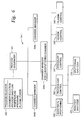
- Figure 6 shows an illustrative block diagram of the hierarchical control structure of the computer program 541 of the microprocessor controller 499.
- a user enters a process set number and process chamber number into a process selector subroutine 542 in response to menus or screens displayed on the CRT monitor by using the light pen interface.
- the process sets are predetermined sets of process parameters necessary to carry out specified processes, and are identified by predefined set numbers.
- Process selector subroutine 542 identifies (i) the desired process chamber in a multi-chamber system, and (ii) the desired set of process parameters needed to operate the process chamber for performing the desired process.
- the process parameters for performing a specific process relate to process conditions such as, for example, process gas composition and flow rates, temperature, pressure, plasma conditions such as RF power levels, and chamber dome temperature, and are provided to the user in the form of a recipe.
- process conditions such as, for example, process gas composition and flow rates, temperature, pressure, plasma conditions such as RF power levels, and chamber dome temperature.
- the parameters specified by the recipe are entered utilizing a light pen/CRT monitor interface (not shown).
- a process sequencer subroutine 543 comprises program code for accepting the identified process chamber and set of process parameters from the process selector subroutine 542, and for controlling operation of the various process chambers. Multiple users can enter process set numbers and process chamber numbers, or a user can enter multiple process set numbers and process chamber numbers, so the sequencer subroutine 543 operates to schedule the selected processes in the desired sequence.
- the sequencer subroutine 543 includes a program code to perform the steps of (i) monitoring the operation of the process chambers to determine if the chambers are being used, (ii) determining what processes are being carried out in the chambers being used, and (iii) executing the desired process based on availability of a process chamber and type of process to be carried out.
- sequencer subroutine 543 can be designed to take into consideration the present condition of the process chamber being used in comparison with the desired process conditions for a selected process, or the "age" of each particular user entered request, or any other relevant factor a system programmer desires to include for determining scheduling priorities.
- sequencer subroutine 543 determines which process chamber and process set combination is going to be executed next, sequencer subroutine 543 causes execution of the process set by passing the particular process set parameters to a chamber manager subroutine 544A-C, which controls multiple processing tasks in CVD chamber 430 and possibly other chambers (not shown) according to tile process set determined by sequencer subroutine 543.
- the sequencer subroutine 543 determines which process chamber and process set combination is going to be executed next, the sequencer subroutine 543 causes execution of the process set by passing the particular process set parameters to the chamber manager subroutines 544A-C which control multiple processing tasks in different process chambers according to the process set determined by the sequencer subroutine 543.
- the chamber manager subroutine 544A comprises program code for controlling CVD process operations, within the described process chamber 430 of Figure 5.
- the chamber manager subroutine 544 also controls execution of various chamber component subroutines or program code modules, which control operation of the chamber components necessary to carry out the selected process set.
- chamber component subroutines are substrate positioning subroutine 545, process gas control subroutine 546, pressure control subroutine 547, heater control subroutine 548, and plasma control subroutine 549.
- chamber manager subroutine 544A selectively schedules or calls the process component subroutines in accordance with the particular process set being executed.
- Chamber manager subroutine 544A Scheduling by chamber manager subroutine 544A is performed in a manner similar to that used by sequencer subroutine 543 in scheduling which process chamber and process set to execute.
- chamber manager subroutine 544A includes steps of monitoring the various chamber components, determining which components need to be operated based on the process parameters for the process set to be executed, and causing execution of a chamber component subroutine responsive to the monitoring and determining steps.
- the following hypothetical examples illustrate the best mode contemplated by the invention.
- the following hypothetical examples illustrate deposition of metal and metal nitride films by precursors of the invention.
- the examples may be performed in a chemical vapor deposition chamber, and in particular, a "CENTURA TxZ" system capable of both thermal decomposition and plasma enhanced chemical vapor deposition processes as described above, and sold by Applied Materials, Inc., Santa Clara, California.
- Precursors of the invention generally have the formula (Cp(R) n ) x MH y-x , for which preferred precursors, such as (Si(CH 3 ) 3 )C 5 H 4 ) 2 TaH 3 , can be formed when Cp is cyclopentadienyl, -(C 5 H 4 ), R is trimethylsilyl, Si(CH 3 ) 3 , n is one, x is two, M is tantalum, y is 5, and y-x is 3.
- Tantalum Film Deposition Thermal Decomposition :
- a tantalum (Ta) film is deposited at a chamber pressure of 150 milliTorr and temperature of 400°C from reactive gases which flow into the reactor as follows: ((Si(CH 3 ) 3 )C 5 H 4 ) 2 TaH 3 , at 25 sccm bis(trimethylsilylcyclopentadienyl) trihydrotantalum Hydrogen, H 2 , at 25 sccm Argon, Ar, at 100 sccm.
- a subsequent plasma treatment at a chamber pressure of 150 milliTorr with 750 W of high frequency power (13 MHz) is applied to the showerhead for contaminant removal from the deposited tantalum layer, the plasma gases flow into the reactor as follows: ((Si(CH 3 ) 3 )C 5 H 4 ) 2 TaH 3 , at 0 sccm bis(trimethylsilylcyclopentadienyl) trihydrotantalum Hydrogen, H 2 , at 25 sccm Argon, Ar, at 125 sccm.
- Tantalum Film Deposition in the Absence of Reactant Gases :
- a tantalum (Ta) film is deposited at a chamber pressure of 150 milliTorr and temperature of 400°C from reactive gases which flow into the reactor as follows: ((Si(CH 3 ) 3 )C 5 H 4 ) 2 TaH 3 , at 25 sccm bis(trimethylsilylcyclopentadienyl) trihydrotantalum Argon, Ar, at 100 sccm.
- a subsequent plasma treatment at a chamber pressure of 150 milliTorr with 750 W of high frequency power (13 MHz) is applied to the showerhead for contaminant removal from the deposited tantalum layer, the plasma gases flow into the reactor as follows: ((Si(CH 3 ) 3 )C 5 H 4 ) 2 TaH 3 , at 0 sccm bis(trimethylsilylcyclopentadienyl) trihydrotantalum Argon, Ar, at 125 sccm.
- Tantalum Film Deposition Vaporized Precursor from a Liquid Delivery System :
- a tantalum (Ta) film is deposited by a vaporized precursor with a 1:1 molar ratio of (C 5 H 5 ) 2 TaH 3 , bis(cyclopentadienyl) trihydrotantalum to hexane solvent at a chamber pressure of 1 Torr and at a temperature of 400°C from vaporized precursors and reactive gases which flow into the reactor as follows: ((Si(CH 3 ) 3 )C 5 H 4 ) 2 TaH 3 , at 25 sccm bis(trimethylsilylcyclopentadienyl) trihydrotantalum Hexane, at 25 sccm Hydrogen, H 2 , at 25 sccm Argon, Ar, at 100 sccm.
- a subsequent plasma treatment at a chamber pressure of 1 Torr with 750 W of high frequency power (13 MHz) is applied to the showerhead for contaminant removal from the deposited tantalum layer, the plasma gases flow into the reactor as follows: ((Si(CH 3 ) 3 )C 5 H 4 ) 2 TaH 3 , at 0 sccm bis(trimethylsilylcyclopentadienyl) trihydrotantalum Hexane, at 0 sccm Hydrogen, H 2 , at 0 sccm Argon, Ar, at 125 sccm.
- Tantalum Film Deposition Plasma Enhanced Decomposition:
- a tantalum (Ta) film containing silicon is deposited at a chamber pressure of 150 milliTorr, temperature of 400°C, and a plasma power of 750 W of high frequency power (13 MHz) from reactive gases which flow into the reactor as follows: ((Si(CH 3 ) 3 )C 5 H 4 ) 2 TaH 3 , at 25 sccm bis(trimethylsilylcyclopentadienyl) trihydrotantalum Hydrogen, H 2 , at 25 sccm Argon, Ar, at 100 sccm.
- a subsequent plasma treatment at a chamber pressure of 150 milliTorr with 750 W of high frequency power (13 MHz) is applied to the showerhead for contaminant removal from the deposited tantalum layer, the plasma gases flow into the reactor as follows: ((Si(CH 3 ) 3 )C 5 H 4 ) 2 TaH 3 , at 0 sccm bis(trimethylsilylcyclopentadienyl) trihydrotantalum Hydrogen, H 2 , at 25 sccm Argon, Ar, at 125 sccm.
- Tantalum Carbon Nitride Film Deposition
- TaCN tantalum carbon nitride
- Tantalum Nitride Film Deposition by Ammonia
- TaN tantalum nitride
- a tantalum nitride (TaN) film is deposited at a chamber pressure of 150 milliTorr and temperature of 400°C from reactive gases which flow into the reactor as follows: ((Si(CH 3 ) 3 )C 5 H 4 ) 2 TaH 3 , at 40 sccm bis(trimethylsilylcyclopentadienyl) trihydrotantalum Ammonia, NH 3 , at 40 sccm Helium, He, at 50 sccm.
- a subsequent plasma treatment at a chamber pressure of 150 milliTorr with 750 W of high frequency power (13 MHz) is applied to the showerhead for contaminant removal from the deposited tantalum nitride layer, the plasma gases flow into the reactor as follows: ((Si(CH 3 ) 3 )C 5 H 4 ) 2 TaH 3 , at 0 sccm bis(trimethylsilylcyclopentadienyl) trihydrotantalum Ammonia, NH 3 , at 0 sccm Helium, He, at 130 sccm.
- Tantalum Silicon Nitride Film Deposition
- TaSiN tantalum nitride
- a tantalum nitride (TaSiN) film is deposited at a chamber pressure of 150 milliTorr and temperature of 400°C from reactive gases which flow into the reactor as follows: ((Si(CH 3 ) 3 )C 5 H 4 ) 2 TaH 3 , at 25 sccm bis(trimethylsilylcyclopentadienyl) trihydrotantalum Nitrogen, N 2 , at 25 sccm Silane, SiH 4 , at 25 sccm Argon, Ar, at 75 sccm.
- a subsequent plasma treatment at a chamber pressure of 150 milliTorr with 750 W of high frequency power (13 MHz) is applied to the showerhead for contaminant removal from the deposited tantalum silicon nitride layer, the plasma gases flow into the reactor as follows: ((Si(CH 3 ) 3 )C 5 H 4 ) 2 TaH 3 , at 0 sccm bis(trimethylsilylcyclopentadienyl) trihydrotantalum Nitrogen, N 2 , at 0 sccm Silane, SiH 4 , at 0 sccm Argon, Ar, at 150 sccm.
- a niobium nitride (Nb 3 N 4 ) film is deposited at a chamber pressure of 150 milliTorr and temperature of 400°C from reactive gases which flow into the reactor as follows: ((Si(CH 3 ) 3 )C 5 H 4 ) 2 NbH 3 , at 40 sccm bis(trimethylsilylcyclopentadienyl) trihydroniobium Ammonia, NH 3 , at 40 sccm Helium, He, at 50 sccm.
- a subsequent plasma treatment at a chamber pressure of 150 milliTorr with 750 W of high frequency power (13 MHz) is applied to the showerhead for contaminant removal from the deposited tantalum nitride layer, the plasma gases flow into the reactor as follows: ((Si(CH 3 ) 3 )C 5 H 4 ) 2 NbH 3 , at 40 sccm bis(trimethylsilylcyclopentadienyl) trihydroniobium Ammonia, NH 3 , at 40 sccm Helium, He, at 90 sccm.
Landscapes
- Chemical & Material Sciences (AREA)
- General Chemical & Material Sciences (AREA)
- Chemical Kinetics & Catalysis (AREA)
- Engineering & Computer Science (AREA)
- Materials Engineering (AREA)
- Mechanical Engineering (AREA)
- Metallurgy (AREA)
- Organic Chemistry (AREA)
- Inorganic Chemistry (AREA)
- Chemical Vapour Deposition (AREA)
- Internal Circuitry In Semiconductor Integrated Circuit Devices (AREA)
- Electrodes Of Semiconductors (AREA)
Applications Claiming Priority (2)
| Application Number | Priority Date | Filing Date | Title |
|---|---|---|---|
| US09/505,638 US6743473B1 (en) | 2000-02-16 | 2000-02-16 | Chemical vapor deposition of barriers from novel precursors |
| US505638 | 2000-02-16 |
Publications (2)
| Publication Number | Publication Date |
|---|---|
| EP1126046A2 true EP1126046A2 (fr) | 2001-08-22 |
| EP1126046A3 EP1126046A3 (fr) | 2003-12-17 |
Family
ID=24011186
Family Applications (1)
| Application Number | Title | Priority Date | Filing Date |
|---|---|---|---|
| EP01103524A Withdrawn EP1126046A3 (fr) | 2000-02-16 | 2001-02-16 | Fabrication de barrières par CVD utilisant des précurseurs nouveaux |
Country Status (5)
| Country | Link |
|---|---|
| US (1) | US6743473B1 (fr) |
| EP (1) | EP1126046A3 (fr) |
| JP (1) | JP4813676B2 (fr) |
| KR (1) | KR100682153B1 (fr) |
| SG (1) | SG84622A1 (fr) |
Cited By (5)
| Publication number | Priority date | Publication date | Assignee | Title |
|---|---|---|---|---|
| US6638810B2 (en) | 2000-02-22 | 2003-10-28 | Applied Materials, Inc. | Tantalum nitride CVD deposition by tantalum oxide densification |
| WO2006028844A1 (fr) * | 2004-09-01 | 2006-03-16 | Applied Materials, Inc. | Procede de depot de films dielectriques a gradient de fonctionnalite par depot chimique en phase a vapeur en utilisant des precurseurs visqueux |
| US7067439B2 (en) | 2002-06-14 | 2006-06-27 | Applied Materials, Inc. | ALD metal oxide deposition process using direct oxidation |
| WO2007085928A3 (fr) * | 2006-01-27 | 2008-03-20 | Air Liquide | Appareil permettant de distribuer de multiples precurseurs |
| EP2498279A1 (fr) * | 2011-03-07 | 2012-09-12 | Altis Semiconductor | Procédé de traitement d'une couche de nitrure de métal oxydée |
Families Citing this family (248)
| Publication number | Priority date | Publication date | Assignee | Title |
|---|---|---|---|---|
| US7253124B2 (en) * | 2000-10-20 | 2007-08-07 | Texas Instruments Incorporated | Process for defect reduction in electrochemical plating |
| US6951804B2 (en) * | 2001-02-02 | 2005-10-04 | Applied Materials, Inc. | Formation of a tantalum-nitride layer |
| US9708707B2 (en) | 2001-09-10 | 2017-07-18 | Asm International N.V. | Nanolayer deposition using bias power treatment |
| GB0129567D0 (en) * | 2001-12-11 | 2002-01-30 | Trikon Technologies Ltd | Diffusion barrier |
| US7138014B2 (en) * | 2002-01-28 | 2006-11-21 | Applied Materials, Inc. | Electroless deposition apparatus |
| US6905622B2 (en) * | 2002-04-03 | 2005-06-14 | Applied Materials, Inc. | Electroless deposition method |
| US20030190426A1 (en) * | 2002-04-03 | 2003-10-09 | Deenesh Padhi | Electroless deposition method |
| US6899816B2 (en) * | 2002-04-03 | 2005-05-31 | Applied Materials, Inc. | Electroless deposition method |
| US7081409B2 (en) * | 2002-07-17 | 2006-07-25 | Samsung Electronics Co., Ltd. | Methods of producing integrated circuit devices utilizing tantalum amine derivatives |
| KR100992803B1 (ko) * | 2002-07-25 | 2010-11-09 | 도쿄엘렉트론가부시키가이샤 | 기판 처리 용기 |
| US6821909B2 (en) * | 2002-10-30 | 2004-11-23 | Applied Materials, Inc. | Post rinse to improve selective deposition of electroless cobalt on copper for ULSI application |
| US9121098B2 (en) | 2003-02-04 | 2015-09-01 | Asm International N.V. | NanoLayer Deposition process for composite films |
| US7713592B2 (en) | 2003-02-04 | 2010-05-11 | Tegal Corporation | Nanolayer deposition process |
| US7311946B2 (en) * | 2003-05-02 | 2007-12-25 | Air Products And Chemicals, Inc. | Methods for depositing metal films on diffusion barrier layers by CVD or ALD processes |
| US7654221B2 (en) * | 2003-10-06 | 2010-02-02 | Applied Materials, Inc. | Apparatus for electroless deposition of metals onto semiconductor substrates |
| US7827930B2 (en) * | 2004-01-26 | 2010-11-09 | Applied Materials, Inc. | Apparatus for electroless deposition of metals onto semiconductor substrates |
| US20070111519A1 (en) * | 2003-10-15 | 2007-05-17 | Applied Materials, Inc. | Integrated electroless deposition system |
| US7064065B2 (en) * | 2003-10-15 | 2006-06-20 | Applied Materials, Inc. | Silver under-layers for electroless cobalt alloys |
| US7465358B2 (en) * | 2003-10-15 | 2008-12-16 | Applied Materials, Inc. | Measurement techniques for controlling aspects of a electroless deposition process |
| WO2005038084A2 (fr) * | 2003-10-17 | 2005-04-28 | Applied Materials, Inc. | Depot autocatalytique selectif a auto-amorçage d'une couche protectrice de cuivre a base d'alliages contenant du cobalt |
| US20050095830A1 (en) * | 2003-10-17 | 2005-05-05 | Applied Materials, Inc. | Selective self-initiating electroless capping of copper with cobalt-containing alloys |
| US7205233B2 (en) * | 2003-11-07 | 2007-04-17 | Applied Materials, Inc. | Method for forming CoWRe alloys by electroless deposition |
| US20060003570A1 (en) * | 2003-12-02 | 2006-01-05 | Arulkumar Shanmugasundram | Method and apparatus for electroless capping with vapor drying |
| US20050170650A1 (en) * | 2004-01-26 | 2005-08-04 | Hongbin Fang | Electroless palladium nitrate activation prior to cobalt-alloy deposition |
| US20050181226A1 (en) * | 2004-01-26 | 2005-08-18 | Applied Materials, Inc. | Method and apparatus for selectively changing thin film composition during electroless deposition in a single chamber |
| US20050161338A1 (en) * | 2004-01-26 | 2005-07-28 | Applied Materials, Inc. | Electroless cobalt alloy deposition process |
| US20050230350A1 (en) * | 2004-02-26 | 2005-10-20 | Applied Materials, Inc. | In-situ dry clean chamber for front end of line fabrication |
| US20050253268A1 (en) * | 2004-04-22 | 2005-11-17 | Shao-Ta Hsu | Method and structure for improving adhesion between intermetal dielectric layer and cap layer |
| US7378744B2 (en) * | 2004-05-10 | 2008-05-27 | Taiwan Semiconductor Manufacturing Company, Ltd. | Plasma treatment at film layer to reduce sheet resistance and to improve via contact resistance |
| US7067409B2 (en) * | 2004-05-10 | 2006-06-27 | Taiwan Semiconductor Manufacturing Company, Ltd. | Plasma treatment at film layer to reduce sheet resistance and to improve via contact resistance |
| JP4642379B2 (ja) * | 2004-05-12 | 2011-03-02 | 東京エレクトロン株式会社 | 排気捕集装置 |
| US8119210B2 (en) | 2004-05-21 | 2012-02-21 | Applied Materials, Inc. | Formation of a silicon oxynitride layer on a high-k dielectric material |
| US20070059929A1 (en) * | 2004-06-25 | 2007-03-15 | Hag-Ju Cho | Method of forming a tantalum carbon nitride layer and method of manufacturing a semiconductor device using the same |
| US20070026621A1 (en) * | 2004-06-25 | 2007-02-01 | Hag-Ju Cho | Non-volatile semiconductor devices and methods of manufacturing the same |
| KR100602087B1 (ko) * | 2004-07-09 | 2006-07-14 | 동부일렉트로닉스 주식회사 | 반도체 소자 및 그 제조방법 |
| US7438949B2 (en) * | 2005-01-27 | 2008-10-21 | Applied Materials, Inc. | Ruthenium containing layer deposition method |
| US20060162658A1 (en) * | 2005-01-27 | 2006-07-27 | Applied Materials, Inc. | Ruthenium layer deposition apparatus and method |
| US20060240187A1 (en) * | 2005-01-27 | 2006-10-26 | Applied Materials, Inc. | Deposition of an intermediate catalytic layer on a barrier layer for copper metallization |
| JP5053543B2 (ja) * | 2005-02-02 | 2012-10-17 | 東ソー株式会社 | タンタル化合物、その製造方法、タンタル含有薄膜、及びその形成方法 |
| US7651934B2 (en) | 2005-03-18 | 2010-01-26 | Applied Materials, Inc. | Process for electroless copper deposition |
| US20060251801A1 (en) * | 2005-03-18 | 2006-11-09 | Weidman Timothy W | In-situ silicidation metallization process |
| WO2006102318A2 (fr) * | 2005-03-18 | 2006-09-28 | Applied Materials, Inc. | Procede de depot autocatalytique sur un contact contenant du silicium ou du siliciure |
| US20060246699A1 (en) * | 2005-03-18 | 2006-11-02 | Weidman Timothy W | Process for electroless copper deposition on a ruthenium seed |
| FI118803B (fi) * | 2005-04-22 | 2008-03-31 | Beneq Oy | Lähde, järjestely lähteen asentamiseksi sekä menetelmä lähteen asentamiseksi ja poistamiseksi |
| US20070001231A1 (en) * | 2005-06-29 | 2007-01-04 | Amberwave Systems Corporation | Material systems for dielectrics and metal electrodes |
| US7432139B2 (en) * | 2005-06-29 | 2008-10-07 | Amberwave Systems Corp. | Methods for forming dielectrics and metal electrodes |
| US20070054046A1 (en) * | 2005-09-06 | 2007-03-08 | Tokyo Electron Limited | Method of forming a tantalum-containing layer from a metalorganic precursor |
| US20070054047A1 (en) * | 2005-09-06 | 2007-03-08 | Tokyo Electron Limited | Method of forming a tantalum-containing layer from a metalorganic precursor |
| US20070071888A1 (en) * | 2005-09-21 | 2007-03-29 | Arulkumar Shanmugasundram | Method and apparatus for forming device features in an integrated electroless deposition system |
| US7582557B2 (en) * | 2005-10-06 | 2009-09-01 | Taiwan Semiconductor Manufacturing Co., Ltd. | Process for low resistance metal cap |
| US7446034B2 (en) * | 2005-10-06 | 2008-11-04 | Taiwan Semiconductor Manufacturing Co., Ltd. | Process for making a metal seed layer |
| US7645710B2 (en) | 2006-03-09 | 2010-01-12 | Applied Materials, Inc. | Method and apparatus for fabricating a high dielectric constant transistor gate using a low energy plasma system |
| US7678710B2 (en) | 2006-03-09 | 2010-03-16 | Applied Materials, Inc. | Method and apparatus for fabricating a high dielectric constant transistor gate using a low energy plasma system |
| US7837838B2 (en) | 2006-03-09 | 2010-11-23 | Applied Materials, Inc. | Method of fabricating a high dielectric constant transistor gate using a low energy plasma apparatus |
| WO2007140813A1 (fr) | 2006-06-02 | 2007-12-13 | L'air Liquide Societe Anonyme Pour L'etude Et L'exploitation Des Procedes Georges Claude | Procédé de formation de films à constante diélectrique élevée à base de nouveaux précurseurs de titane, de zirconium et d'hafnium et utilisation desdits films pour la fabrication de semi-conducteurs |
| US7959986B2 (en) * | 2006-08-09 | 2011-06-14 | Praxair Technology, Inc. | Organometallic compounds, processes for the preparation thereof and methods of use thereof |
| TWI435376B (zh) | 2006-09-26 | 2014-04-21 | 應用材料股份有限公司 | 用於缺陷鈍化之高k閘極堆疊的氟電漿處理 |
| EP1916253A1 (fr) * | 2006-10-26 | 2008-04-30 | L'AIR LIQUIDE, Société Anonyme pour l'Etude et l'Exploitation des Procédés Georges Claude | Précurseurs à base d'un métal du groupe V, et leur utilisation pour le dépôt de couche mince contenant du metal |
| US7682891B2 (en) * | 2006-12-28 | 2010-03-23 | Intel Corporation | Tunable gate electrode work function material for transistor applications |
| KR100857590B1 (ko) * | 2007-02-12 | 2008-09-09 | 충남대학교산학협력단 | 연성 폴리머 기판 위에 상온 화학증착법 |
| US7777344B2 (en) | 2007-04-11 | 2010-08-17 | Taiwan Semiconductor Manufacturing Company, Ltd. | Transitional interface between metal and dielectric in interconnect structures |
| US7883745B2 (en) | 2007-07-30 | 2011-02-08 | Micron Technology, Inc. | Chemical vaporizer for material deposition systems and associated methods |
| US7867900B2 (en) * | 2007-09-28 | 2011-01-11 | Applied Materials, Inc. | Aluminum contact integration on cobalt silicide junction |
| US20090130466A1 (en) * | 2007-11-16 | 2009-05-21 | Air Products And Chemicals, Inc. | Deposition Of Metal Films On Diffusion Layers By Atomic Layer Deposition And Organometallic Precursor Complexes Therefor |
| US8969195B2 (en) * | 2008-02-22 | 2015-03-03 | International Business Machines Corporation | Methods of manufacturing semiconductor devices and a semiconductor structure |
| WO2009106433A1 (fr) | 2008-02-27 | 2009-09-03 | L'air Liquide Societe Anonyme Pour L'etude Et L'exploitation Des Procedes Georges Claude | Procédé de formation d'une couche à teneur en titane sur un substrat à l'aide d'un procédé de déposition en couches atomiques (ald) |
| US20090269939A1 (en) * | 2008-04-25 | 2009-10-29 | Asm International, N.V. | Cyclical oxidation process |
| CN102112654B (zh) | 2008-08-01 | 2013-03-20 | 乔治洛德方法研究和开发液化空气有限公司 | 在基质上形成含钽层的方法 |
| JP2011249351A (ja) * | 2008-09-19 | 2011-12-08 | Panasonic Corp | 記憶素子及び記憶装置 |
| ATE535534T1 (de) * | 2008-10-07 | 2011-12-15 | Air Liquide | Metall-organische niobium- und vanadium-vorläufer zur dünnschichtablagerung |
| US9127340B2 (en) * | 2009-02-13 | 2015-09-08 | Asm International N.V. | Selective oxidation process |
| US8889565B2 (en) * | 2009-02-13 | 2014-11-18 | Asm International N.V. | Selective removal of oxygen from metal-containing materials |
| US7829457B2 (en) * | 2009-02-20 | 2010-11-09 | Asm International N.V. | Protection of conductors from oxidation in deposition chambers |
| US8491720B2 (en) * | 2009-04-10 | 2013-07-23 | Applied Materials, Inc. | HVPE precursor source hardware |
| US8512809B2 (en) | 2010-03-31 | 2013-08-20 | General Electric Company | Method of processing multilayer film |
| US8507388B2 (en) | 2010-04-26 | 2013-08-13 | Asm International N.V. | Prevention of oxidation of substrate surfaces in process chambers |
| US9324576B2 (en) | 2010-05-27 | 2016-04-26 | Applied Materials, Inc. | Selective etch for silicon films |
| US10283321B2 (en) | 2011-01-18 | 2019-05-07 | Applied Materials, Inc. | Semiconductor processing system and methods using capacitively coupled plasma |
| US8771539B2 (en) | 2011-02-22 | 2014-07-08 | Applied Materials, Inc. | Remotely-excited fluorine and water vapor etch |
| US9064815B2 (en) | 2011-03-14 | 2015-06-23 | Applied Materials, Inc. | Methods for etch of metal and metal-oxide films |
| US8999856B2 (en) | 2011-03-14 | 2015-04-07 | Applied Materials, Inc. | Methods for etch of sin films |
| US8771536B2 (en) | 2011-08-01 | 2014-07-08 | Applied Materials, Inc. | Dry-etch for silicon-and-carbon-containing films |
| US8679982B2 (en) | 2011-08-26 | 2014-03-25 | Applied Materials, Inc. | Selective suppression of dry-etch rate of materials containing both silicon and oxygen |
| US8679983B2 (en) | 2011-09-01 | 2014-03-25 | Applied Materials, Inc. | Selective suppression of dry-etch rate of materials containing both silicon and nitrogen |
| US8927390B2 (en) | 2011-09-26 | 2015-01-06 | Applied Materials, Inc. | Intrench profile |
| US8808563B2 (en) | 2011-10-07 | 2014-08-19 | Applied Materials, Inc. | Selective etch of silicon by way of metastable hydrogen termination |
| WO2013070436A1 (fr) | 2011-11-08 | 2013-05-16 | Applied Materials, Inc. | Procédés de réduction de dislocation de substrat durant un traitement de remplissage d'intervalle |
| KR101930849B1 (ko) * | 2011-12-28 | 2018-12-20 | 삼성디스플레이 주식회사 | 박막 증착 장치 및 그것을 이용한 박막 증착 방법 |
| US9267739B2 (en) | 2012-07-18 | 2016-02-23 | Applied Materials, Inc. | Pedestal with multi-zone temperature control and multiple purge capabilities |
| US9373517B2 (en) | 2012-08-02 | 2016-06-21 | Applied Materials, Inc. | Semiconductor processing with DC assisted RF power for improved control |
| US9034770B2 (en) | 2012-09-17 | 2015-05-19 | Applied Materials, Inc. | Differential silicon oxide etch |
| US9023734B2 (en) | 2012-09-18 | 2015-05-05 | Applied Materials, Inc. | Radical-component oxide etch |
| US9390937B2 (en) | 2012-09-20 | 2016-07-12 | Applied Materials, Inc. | Silicon-carbon-nitride selective etch |
| US9132436B2 (en) | 2012-09-21 | 2015-09-15 | Applied Materials, Inc. | Chemical control features in wafer process equipment |
| US8765574B2 (en) | 2012-11-09 | 2014-07-01 | Applied Materials, Inc. | Dry etch process |
| US8969212B2 (en) | 2012-11-20 | 2015-03-03 | Applied Materials, Inc. | Dry-etch selectivity |
| US8980763B2 (en) | 2012-11-30 | 2015-03-17 | Applied Materials, Inc. | Dry-etch for selective tungsten removal |
| US9064816B2 (en) | 2012-11-30 | 2015-06-23 | Applied Materials, Inc. | Dry-etch for selective oxidation removal |
| US9111877B2 (en) | 2012-12-18 | 2015-08-18 | Applied Materials, Inc. | Non-local plasma oxide etch |
| US8921234B2 (en) | 2012-12-21 | 2014-12-30 | Applied Materials, Inc. | Selective titanium nitride etching |
| US10256079B2 (en) | 2013-02-08 | 2019-04-09 | Applied Materials, Inc. | Semiconductor processing systems having multiple plasma configurations |
| US9362130B2 (en) | 2013-03-01 | 2016-06-07 | Applied Materials, Inc. | Enhanced etching processes using remote plasma sources |
| US9040422B2 (en) | 2013-03-05 | 2015-05-26 | Applied Materials, Inc. | Selective titanium nitride removal |
| US8801952B1 (en) | 2013-03-07 | 2014-08-12 | Applied Materials, Inc. | Conformal oxide dry etch |
| US10170282B2 (en) | 2013-03-08 | 2019-01-01 | Applied Materials, Inc. | Insulated semiconductor faceplate designs |
| US20140271097A1 (en) | 2013-03-15 | 2014-09-18 | Applied Materials, Inc. | Processing systems and methods for halide scavenging |
| US8895449B1 (en) | 2013-05-16 | 2014-11-25 | Applied Materials, Inc. | Delicate dry clean |
| US9114438B2 (en) | 2013-05-21 | 2015-08-25 | Applied Materials, Inc. | Copper residue chamber clean |
| US9493879B2 (en) | 2013-07-12 | 2016-11-15 | Applied Materials, Inc. | Selective sputtering for pattern transfer |
| US9773648B2 (en) | 2013-08-30 | 2017-09-26 | Applied Materials, Inc. | Dual discharge modes operation for remote plasma |
| US8956980B1 (en) | 2013-09-16 | 2015-02-17 | Applied Materials, Inc. | Selective etch of silicon nitride |
| US8951429B1 (en) | 2013-10-29 | 2015-02-10 | Applied Materials, Inc. | Tungsten oxide processing |
| US9576809B2 (en) | 2013-11-04 | 2017-02-21 | Applied Materials, Inc. | Etch suppression with germanium |
| US9236265B2 (en) | 2013-11-04 | 2016-01-12 | Applied Materials, Inc. | Silicon germanium processing |
| US9520303B2 (en) | 2013-11-12 | 2016-12-13 | Applied Materials, Inc. | Aluminum selective etch |
| US9245762B2 (en) | 2013-12-02 | 2016-01-26 | Applied Materials, Inc. | Procedure for etch rate consistency |
| US9117855B2 (en) | 2013-12-04 | 2015-08-25 | Applied Materials, Inc. | Polarity control for remote plasma |
| US9287095B2 (en) | 2013-12-17 | 2016-03-15 | Applied Materials, Inc. | Semiconductor system assemblies and methods of operation |
| US9263278B2 (en) | 2013-12-17 | 2016-02-16 | Applied Materials, Inc. | Dopant etch selectivity control |
| US9190293B2 (en) | 2013-12-18 | 2015-11-17 | Applied Materials, Inc. | Even tungsten etch for high aspect ratio trenches |
| US9287134B2 (en) | 2014-01-17 | 2016-03-15 | Applied Materials, Inc. | Titanium oxide etch |
| US9293568B2 (en) | 2014-01-27 | 2016-03-22 | Applied Materials, Inc. | Method of fin patterning |
| US9396989B2 (en) | 2014-01-27 | 2016-07-19 | Applied Materials, Inc. | Air gaps between copper lines |
| US9385028B2 (en) | 2014-02-03 | 2016-07-05 | Applied Materials, Inc. | Air gap process |
| US9499898B2 (en) | 2014-03-03 | 2016-11-22 | Applied Materials, Inc. | Layered thin film heater and method of fabrication |
| US9299575B2 (en) | 2014-03-17 | 2016-03-29 | Applied Materials, Inc. | Gas-phase tungsten etch |
| US9299537B2 (en) | 2014-03-20 | 2016-03-29 | Applied Materials, Inc. | Radial waveguide systems and methods for post-match control of microwaves |
| US9299538B2 (en) | 2014-03-20 | 2016-03-29 | Applied Materials, Inc. | Radial waveguide systems and methods for post-match control of microwaves |
| US9136273B1 (en) | 2014-03-21 | 2015-09-15 | Applied Materials, Inc. | Flash gate air gap |
| US9903020B2 (en) | 2014-03-31 | 2018-02-27 | Applied Materials, Inc. | Generation of compact alumina passivation layers on aluminum plasma equipment components |
| US9269590B2 (en) | 2014-04-07 | 2016-02-23 | Applied Materials, Inc. | Spacer formation |
| US9309598B2 (en) | 2014-05-28 | 2016-04-12 | Applied Materials, Inc. | Oxide and metal removal |
| US9847289B2 (en) | 2014-05-30 | 2017-12-19 | Applied Materials, Inc. | Protective via cap for improved interconnect performance |
| US9378969B2 (en) | 2014-06-19 | 2016-06-28 | Applied Materials, Inc. | Low temperature gas-phase carbon removal |
| US9406523B2 (en) | 2014-06-19 | 2016-08-02 | Applied Materials, Inc. | Highly selective doped oxide removal method |
| US9425058B2 (en) | 2014-07-24 | 2016-08-23 | Applied Materials, Inc. | Simplified litho-etch-litho-etch process |
| US9378978B2 (en) | 2014-07-31 | 2016-06-28 | Applied Materials, Inc. | Integrated oxide recess and floating gate fin trimming |
| US9496167B2 (en) | 2014-07-31 | 2016-11-15 | Applied Materials, Inc. | Integrated bit-line airgap formation and gate stack post clean |
| US9159606B1 (en) | 2014-07-31 | 2015-10-13 | Applied Materials, Inc. | Metal air gap |
| US9165786B1 (en) | 2014-08-05 | 2015-10-20 | Applied Materials, Inc. | Integrated oxide and nitride recess for better channel contact in 3D architectures |
| US9659753B2 (en) | 2014-08-07 | 2017-05-23 | Applied Materials, Inc. | Grooved insulator to reduce leakage current |
| US9553102B2 (en) | 2014-08-19 | 2017-01-24 | Applied Materials, Inc. | Tungsten separation |
| US9355856B2 (en) | 2014-09-12 | 2016-05-31 | Applied Materials, Inc. | V trench dry etch |
| US9478434B2 (en) | 2014-09-24 | 2016-10-25 | Applied Materials, Inc. | Chlorine-based hardmask removal |
| US9368364B2 (en) | 2014-09-24 | 2016-06-14 | Applied Materials, Inc. | Silicon etch process with tunable selectivity to SiO2 and other materials |
| US9613822B2 (en) | 2014-09-25 | 2017-04-04 | Applied Materials, Inc. | Oxide etch selectivity enhancement |
| US9966240B2 (en) | 2014-10-14 | 2018-05-08 | Applied Materials, Inc. | Systems and methods for internal surface conditioning assessment in plasma processing equipment |
| US9355922B2 (en) | 2014-10-14 | 2016-05-31 | Applied Materials, Inc. | Systems and methods for internal surface conditioning in plasma processing equipment |
| US11637002B2 (en) | 2014-11-26 | 2023-04-25 | Applied Materials, Inc. | Methods and systems to enhance process uniformity |
| US9299583B1 (en) | 2014-12-05 | 2016-03-29 | Applied Materials, Inc. | Aluminum oxide selective etch |
| US10224210B2 (en) | 2014-12-09 | 2019-03-05 | Applied Materials, Inc. | Plasma processing system with direct outlet toroidal plasma source |
| US10573496B2 (en) | 2014-12-09 | 2020-02-25 | Applied Materials, Inc. | Direct outlet toroidal plasma source |
| US9499571B2 (en) | 2014-12-23 | 2016-11-22 | L'Air Liquide, Société Anonyme pour l'Etude et l'Exploitation des Procédés Georges Claude | Germanium- and zirconium-containing compositions for vapor deposition of zirconium-containing films |
| US9502258B2 (en) | 2014-12-23 | 2016-11-22 | Applied Materials, Inc. | Anisotropic gap etch |
| US9663547B2 (en) | 2014-12-23 | 2017-05-30 | L'Air Liquide, Société Anonyme pour l'Etude et l'Exploitation des Procédés Georges Claude | Silicon- and Zirconium-containing compositions for vapor deposition of Zirconium-containing films |
| US9343272B1 (en) | 2015-01-08 | 2016-05-17 | Applied Materials, Inc. | Self-aligned process |
| US11257693B2 (en) | 2015-01-09 | 2022-02-22 | Applied Materials, Inc. | Methods and systems to improve pedestal temperature control |
| US9373522B1 (en) | 2015-01-22 | 2016-06-21 | Applied Mateials, Inc. | Titanium nitride removal |
| US9449846B2 (en) | 2015-01-28 | 2016-09-20 | Applied Materials, Inc. | Vertical gate separation |
| US20160225652A1 (en) | 2015-02-03 | 2016-08-04 | Applied Materials, Inc. | Low temperature chuck for plasma processing systems |
| US9728437B2 (en) | 2015-02-03 | 2017-08-08 | Applied Materials, Inc. | High temperature chuck for plasma processing systems |
| US9881805B2 (en) | 2015-03-02 | 2018-01-30 | Applied Materials, Inc. | Silicon selective removal |
| US9859124B2 (en) * | 2015-04-17 | 2018-01-02 | Taiwan Semiconductor Manufacturing Company Ltd | Method of manufacturing semiconductor device with recess |
| US9691645B2 (en) | 2015-08-06 | 2017-06-27 | Applied Materials, Inc. | Bolted wafer chuck thermal management systems and methods for wafer processing systems |
| US9741593B2 (en) | 2015-08-06 | 2017-08-22 | Applied Materials, Inc. | Thermal management systems and methods for wafer processing systems |
| US9349605B1 (en) | 2015-08-07 | 2016-05-24 | Applied Materials, Inc. | Oxide etch selectivity systems and methods |
| US10504700B2 (en) | 2015-08-27 | 2019-12-10 | Applied Materials, Inc. | Plasma etching systems and methods with secondary plasma injection |
| WO2017111814A1 (fr) * | 2015-12-26 | 2017-06-29 | Intel Corporation | Interconnexion à faible résistance |
| US10504754B2 (en) | 2016-05-19 | 2019-12-10 | Applied Materials, Inc. | Systems and methods for improved semiconductor etching and component protection |
| US10522371B2 (en) | 2016-05-19 | 2019-12-31 | Applied Materials, Inc. | Systems and methods for improved semiconductor etching and component protection |
| US9865484B1 (en) | 2016-06-29 | 2018-01-09 | Applied Materials, Inc. | Selective etch using material modification and RF pulsing |
| US10629473B2 (en) | 2016-09-09 | 2020-04-21 | Applied Materials, Inc. | Footing removal for nitride spacer |
| US10062575B2 (en) | 2016-09-09 | 2018-08-28 | Applied Materials, Inc. | Poly directional etch by oxidation |
| US9721789B1 (en) | 2016-10-04 | 2017-08-01 | Applied Materials, Inc. | Saving ion-damaged spacers |
| US9934942B1 (en) | 2016-10-04 | 2018-04-03 | Applied Materials, Inc. | Chamber with flow-through source |
| US10062585B2 (en) | 2016-10-04 | 2018-08-28 | Applied Materials, Inc. | Oxygen compatible plasma source |
| US10546729B2 (en) | 2016-10-04 | 2020-01-28 | Applied Materials, Inc. | Dual-channel showerhead with improved profile |
| US10062579B2 (en) | 2016-10-07 | 2018-08-28 | Applied Materials, Inc. | Selective SiN lateral recess |
| US9947549B1 (en) | 2016-10-10 | 2018-04-17 | Applied Materials, Inc. | Cobalt-containing material removal |
| US10106568B2 (en) | 2016-10-28 | 2018-10-23 | L'Air Liquide, Société Anonyme pour l'Etude et l'Exploitation des Procédés Georges Claude | Hafnium-containing film forming compositions for vapor deposition of hafnium-containing films |
| US9768034B1 (en) | 2016-11-11 | 2017-09-19 | Applied Materials, Inc. | Removal methods for high aspect ratio structures |
| US10163696B2 (en) | 2016-11-11 | 2018-12-25 | Applied Materials, Inc. | Selective cobalt removal for bottom up gapfill |
| US10026621B2 (en) | 2016-11-14 | 2018-07-17 | Applied Materials, Inc. | SiN spacer profile patterning |
| US10242908B2 (en) | 2016-11-14 | 2019-03-26 | Applied Materials, Inc. | Airgap formation with damage-free copper |
| US10566206B2 (en) | 2016-12-27 | 2020-02-18 | Applied Materials, Inc. | Systems and methods for anisotropic material breakthrough |
| US10403507B2 (en) | 2017-02-03 | 2019-09-03 | Applied Materials, Inc. | Shaped etch profile with oxidation |
| US10431429B2 (en) | 2017-02-03 | 2019-10-01 | Applied Materials, Inc. | Systems and methods for radial and azimuthal control of plasma uniformity |
| US10043684B1 (en) | 2017-02-06 | 2018-08-07 | Applied Materials, Inc. | Self-limiting atomic thermal etching systems and methods |
| US10319739B2 (en) | 2017-02-08 | 2019-06-11 | Applied Materials, Inc. | Accommodating imperfectly aligned memory holes |
| US10943834B2 (en) | 2017-03-13 | 2021-03-09 | Applied Materials, Inc. | Replacement contact process |
| US11631580B2 (en) | 2017-03-15 | 2023-04-18 | Versum Materials Us, Llc | Formulation for deposition of silicon doped hafnium oxide as ferroelectric materials |
| US11081337B2 (en) * | 2017-03-15 | 2021-08-03 | Versum Materials U.S., LLC | Formulation for deposition of silicon doped hafnium oxide as ferroelectric materials |
| US11193206B2 (en) * | 2017-03-15 | 2021-12-07 | Versum Materials Us, Llc | Formulation for deposition of silicon doped hafnium oxide as ferroelectric materials |
| US10319649B2 (en) | 2017-04-11 | 2019-06-11 | Applied Materials, Inc. | Optical emission spectroscopy (OES) for remote plasma monitoring |
| JP7176860B6 (ja) | 2017-05-17 | 2022-12-16 | アプライド マテリアルズ インコーポレイテッド | 前駆体の流れを改善する半導体処理チャンバ |
| US11276559B2 (en) | 2017-05-17 | 2022-03-15 | Applied Materials, Inc. | Semiconductor processing chamber for multiple precursor flow |
| US11276590B2 (en) | 2017-05-17 | 2022-03-15 | Applied Materials, Inc. | Multi-zone semiconductor substrate supports |
| US10049891B1 (en) | 2017-05-31 | 2018-08-14 | Applied Materials, Inc. | Selective in situ cobalt residue removal |
| US10497579B2 (en) | 2017-05-31 | 2019-12-03 | Applied Materials, Inc. | Water-free etching methods |
| US10920320B2 (en) | 2017-06-16 | 2021-02-16 | Applied Materials, Inc. | Plasma health determination in semiconductor substrate processing reactors |
| US10821519B2 (en) | 2017-06-23 | 2020-11-03 | General Electric Company | Laser shock peening within an additive manufacturing process |
| US11851763B2 (en) | 2017-06-23 | 2023-12-26 | General Electric Company | Chemical vapor deposition during additive manufacturing |
| US10821718B2 (en) | 2017-06-23 | 2020-11-03 | General Electric Company | Selective powder processing during powder bed additive manufacturing |
| US10541246B2 (en) | 2017-06-26 | 2020-01-21 | Applied Materials, Inc. | 3D flash memory cells which discourage cross-cell electrical tunneling |
| US10727080B2 (en) | 2017-07-07 | 2020-07-28 | Applied Materials, Inc. | Tantalum-containing material removal |
| US10541184B2 (en) | 2017-07-11 | 2020-01-21 | Applied Materials, Inc. | Optical emission spectroscopic techniques for monitoring etching |
| US10354889B2 (en) | 2017-07-17 | 2019-07-16 | Applied Materials, Inc. | Non-halogen etching of silicon-containing materials |
| US10170336B1 (en) | 2017-08-04 | 2019-01-01 | Applied Materials, Inc. | Methods for anisotropic control of selective silicon removal |
| US10043674B1 (en) | 2017-08-04 | 2018-08-07 | Applied Materials, Inc. | Germanium etching systems and methods |
| US10297458B2 (en) | 2017-08-07 | 2019-05-21 | Applied Materials, Inc. | Process window widening using coated parts in plasma etch processes |
| US10510547B2 (en) | 2017-09-13 | 2019-12-17 | Applied Materials, Inc. | Metal and metal-derived films |
| US10128086B1 (en) | 2017-10-24 | 2018-11-13 | Applied Materials, Inc. | Silicon pretreatment for nitride removal |
| US10283324B1 (en) | 2017-10-24 | 2019-05-07 | Applied Materials, Inc. | Oxygen treatment for nitride etching |
| US10381315B2 (en) * | 2017-11-16 | 2019-08-13 | Samsung Electronics Co., Ltd. | Method and system for providing a reverse-engineering resistant hardware embedded security module |
| US10256112B1 (en) | 2017-12-08 | 2019-04-09 | Applied Materials, Inc. | Selective tungsten removal |
| US10903054B2 (en) | 2017-12-19 | 2021-01-26 | Applied Materials, Inc. | Multi-zone gas distribution systems and methods |
| US11328909B2 (en) | 2017-12-22 | 2022-05-10 | Applied Materials, Inc. | Chamber conditioning and removal processes |
| US10854426B2 (en) | 2018-01-08 | 2020-12-01 | Applied Materials, Inc. | Metal recess for semiconductor structures |
| US10679870B2 (en) | 2018-02-15 | 2020-06-09 | Applied Materials, Inc. | Semiconductor processing chamber multistage mixing apparatus |
| US10964512B2 (en) | 2018-02-15 | 2021-03-30 | Applied Materials, Inc. | Semiconductor processing chamber multistage mixing apparatus and methods |
| TWI766433B (zh) | 2018-02-28 | 2022-06-01 | 美商應用材料股份有限公司 | 形成氣隙的系統及方法 |
| US10593560B2 (en) | 2018-03-01 | 2020-03-17 | Applied Materials, Inc. | Magnetic induction plasma source for semiconductor processes and equipment |
| US10504834B2 (en) * | 2018-03-01 | 2019-12-10 | Taiwan Semiconductor Manufacturing Co., Ltd. | Contact structure and the method of forming the same |
| US10319600B1 (en) | 2018-03-12 | 2019-06-11 | Applied Materials, Inc. | Thermal silicon etch |
| US10497573B2 (en) | 2018-03-13 | 2019-12-03 | Applied Materials, Inc. | Selective atomic layer etching of semiconductor materials |
| US10573527B2 (en) | 2018-04-06 | 2020-02-25 | Applied Materials, Inc. | Gas-phase selective etching systems and methods |
| US10490406B2 (en) | 2018-04-10 | 2019-11-26 | Appled Materials, Inc. | Systems and methods for material breakthrough |
| US10699879B2 (en) | 2018-04-17 | 2020-06-30 | Applied Materials, Inc. | Two piece electrode assembly with gap for plasma control |
| US10886137B2 (en) | 2018-04-30 | 2021-01-05 | Applied Materials, Inc. | Selective nitride removal |
| US10872778B2 (en) | 2018-07-06 | 2020-12-22 | Applied Materials, Inc. | Systems and methods utilizing solid-phase etchants |
| US10755941B2 (en) | 2018-07-06 | 2020-08-25 | Applied Materials, Inc. | Self-limiting selective etching systems and methods |
| US10672642B2 (en) | 2018-07-24 | 2020-06-02 | Applied Materials, Inc. | Systems and methods for pedestal configuration |
| US11021792B2 (en) * | 2018-08-17 | 2021-06-01 | Lam Research Corporation | Symmetric precursor delivery |
| US11049755B2 (en) | 2018-09-14 | 2021-06-29 | Applied Materials, Inc. | Semiconductor substrate supports with embedded RF shield |
| US10892198B2 (en) | 2018-09-14 | 2021-01-12 | Applied Materials, Inc. | Systems and methods for improved performance in semiconductor processing |
| US11062887B2 (en) | 2018-09-17 | 2021-07-13 | Applied Materials, Inc. | High temperature RF heater pedestals |
| US11417534B2 (en) | 2018-09-21 | 2022-08-16 | Applied Materials, Inc. | Selective material removal |
| US11682560B2 (en) | 2018-10-11 | 2023-06-20 | Applied Materials, Inc. | Systems and methods for hafnium-containing film removal |
| US11121002B2 (en) | 2018-10-24 | 2021-09-14 | Applied Materials, Inc. | Systems and methods for etching metals and metal derivatives |
| US11437242B2 (en) | 2018-11-27 | 2022-09-06 | Applied Materials, Inc. | Selective removal of silicon-containing materials |
| US11721527B2 (en) | 2019-01-07 | 2023-08-08 | Applied Materials, Inc. | Processing chamber mixing systems |
| US10920319B2 (en) | 2019-01-11 | 2021-02-16 | Applied Materials, Inc. | Ceramic showerheads with conductive electrodes |
| WO2020251696A1 (fr) | 2019-06-10 | 2020-12-17 | Applied Materials, Inc. | Système de traitement pour former des couches |
| US11420259B2 (en) | 2019-11-06 | 2022-08-23 | General Electric Company | Mated components and method and system therefore |
| CN113380761A (zh) * | 2021-05-13 | 2021-09-10 | 中国科学院微电子研究所 | 半导体器件及其制备方法 |
| CN113380763A (zh) * | 2021-05-13 | 2021-09-10 | 中国科学院微电子研究所 | 一种铜互连结构及其制备方法 |
| US12344932B2 (en) * | 2022-01-21 | 2025-07-01 | X-Energy, Llc | Deposition of ceramic layers using liquid organometallic precursors |
| US20240087881A1 (en) * | 2022-08-26 | 2024-03-14 | Applied Materials, Inc. | Systems and methods for depositing low-k dielectric films |
Family Cites Families (16)
| Publication number | Priority date | Publication date | Assignee | Title |
|---|---|---|---|---|
| US3288829A (en) * | 1961-01-19 | 1966-11-29 | Ethyl Corp | Process for preparing cyclopentadienyl group vb and vib metal hydrides |
| DE3379059D1 (en) | 1982-10-19 | 1989-03-02 | Secr Defence Brit | Organometallic chemical vapour deposition of films |
| EP0174743A3 (fr) * | 1984-09-05 | 1988-06-08 | Morton Thiokol, Inc. | Procédé de dépôt de films minces de nitrures de métaux de transition |
| US4992305A (en) | 1988-06-22 | 1991-02-12 | Georgia Tech Research Corporation | Chemical vapor deposition of transistion metals |
| US5130172A (en) * | 1988-10-21 | 1992-07-14 | The Regents Of The University Of California | Low temperature organometallic deposition of metals |
| US5403620A (en) | 1992-10-13 | 1995-04-04 | Regents Of The University Of California | Catalysis in organometallic CVD of thin metal films |
| US6251758B1 (en) * | 1994-11-14 | 2001-06-26 | Applied Materials, Inc. | Construction of a film on a semiconductor wafer |
| GB9502870D0 (en) | 1995-02-14 | 1995-04-05 | Zeneca Ltd | Chiral compounds |
| JP2728025B2 (ja) * | 1995-04-13 | 1998-03-18 | 日本電気株式会社 | 半導体装置の製造方法 |
| US5856236A (en) | 1996-06-14 | 1999-01-05 | Micron Technology, Inc. | Method of depositing a smooth conformal aluminum film on a refractory metal nitride layer |
| US6153519A (en) * | 1997-03-31 | 2000-11-28 | Motorola, Inc. | Method of forming a barrier layer |
| US6348376B2 (en) * | 1997-09-29 | 2002-02-19 | Samsung Electronics Co., Ltd. | Method of forming metal nitride film by chemical vapor deposition and method of forming metal contact and capacitor of semiconductor device using the same |
| US6015917A (en) * | 1998-01-23 | 2000-01-18 | Advanced Technology Materials, Inc. | Tantalum amide precursors for deposition of tantalum nitride on a substrate |
| US6099903A (en) | 1999-05-19 | 2000-08-08 | Research Foundation Of State University Of New York | MOCVD processes using precursors based on organometalloid ligands |
| US6238734B1 (en) | 1999-07-08 | 2001-05-29 | Air Products And Chemicals, Inc. | Liquid precursor mixtures for deposition of multicomponent metal containing materials |
| US6491978B1 (en) * | 2000-07-10 | 2002-12-10 | Applied Materials, Inc. | Deposition of CVD layers for copper metallization using novel metal organic chemical vapor deposition (MOCVD) precursors |
-
2000
- 2000-02-16 US US09/505,638 patent/US6743473B1/en not_active Expired - Fee Related
-
2001
- 2001-02-16 SG SG200100858A patent/SG84622A1/en unknown
- 2001-02-16 KR KR1020010007758A patent/KR100682153B1/ko not_active Expired - Fee Related
- 2001-02-16 EP EP01103524A patent/EP1126046A3/fr not_active Withdrawn
- 2001-02-16 JP JP2001086383A patent/JP4813676B2/ja not_active Expired - Fee Related
Cited By (8)
| Publication number | Priority date | Publication date | Assignee | Title |
|---|---|---|---|---|
| US6638810B2 (en) | 2000-02-22 | 2003-10-28 | Applied Materials, Inc. | Tantalum nitride CVD deposition by tantalum oxide densification |
| US7067439B2 (en) | 2002-06-14 | 2006-06-27 | Applied Materials, Inc. | ALD metal oxide deposition process using direct oxidation |
| WO2006028844A1 (fr) * | 2004-09-01 | 2006-03-16 | Applied Materials, Inc. | Procede de depot de films dielectriques a gradient de fonctionnalite par depot chimique en phase a vapeur en utilisant des precurseurs visqueux |
| US7166544B2 (en) | 2004-09-01 | 2007-01-23 | Applied Materials, Inc. | Method to deposit functionally graded dielectric films via chemical vapor deposition using viscous precursors |
| US7802538B2 (en) | 2004-09-01 | 2010-09-28 | Applied Materials, Inc. | Method to deposit functionally graded dielectric films via chemical vapor deposition using viscous precursors |
| WO2007085928A3 (fr) * | 2006-01-27 | 2008-03-20 | Air Liquide | Appareil permettant de distribuer de multiples precurseurs |
| EP2498279A1 (fr) * | 2011-03-07 | 2012-09-12 | Altis Semiconductor | Procédé de traitement d'une couche de nitrure de métal oxydée |
| FR2972563A1 (fr) * | 2011-03-07 | 2012-09-14 | Altis Semiconductor Snc | Procédé de traitement d'une couche de nitrure de métal oxydée |
Also Published As
| Publication number | Publication date |
|---|---|
| JP2001329367A (ja) | 2001-11-27 |
| JP4813676B2 (ja) | 2011-11-09 |
| KR100682153B1 (ko) | 2007-02-12 |
| KR20010082706A (ko) | 2001-08-30 |
| US6743473B1 (en) | 2004-06-01 |
| SG84622A1 (en) | 2001-11-20 |
| EP1126046A3 (fr) | 2003-12-17 |
Similar Documents
| Publication | Publication Date | Title |
|---|---|---|
| US6743473B1 (en) | Chemical vapor deposition of barriers from novel precursors | |
| US6475902B1 (en) | Chemical vapor deposition of niobium barriers for copper metallization | |
| US6491978B1 (en) | Deposition of CVD layers for copper metallization using novel metal organic chemical vapor deposition (MOCVD) precursors | |
| US5993916A (en) | Method for substrate processing with improved throughput and yield | |
| US10804144B2 (en) | Deposition of aluminum oxide etch stop layers | |
| US6211065B1 (en) | Method of depositing and amorphous fluorocarbon film using HDP-CVD | |
| US6624064B1 (en) | Chamber seasoning method to improve adhesion of F-containing dielectric film to metal for VLSI application | |
| US6319766B1 (en) | Method of tantalum nitride deposition by tantalum oxide densification | |
| US6656831B1 (en) | Plasma-enhanced chemical vapor deposition of a metal nitride layer | |
| US6323119B1 (en) | CVD deposition method to improve adhesion of F-containing dielectric metal lines for VLSI application | |
| JP4808330B2 (ja) | プロセスガス配給装置及び処理チャンバ | |
| JP2026009976A (ja) | 半導体装置の製造における実質的に炭素を含まないモリブデン含有膜およびタングステン含有膜 | |
| WO2001066819A2 (fr) | Procedes de preparation de films en ruthenium metal | |
| EP1122775A2 (fr) | Traitement d'une pile de nitrure de métal/métal | |
| WO2002079537A2 (fr) | Depot chimique en phase vapeur de w avec nucleation de tungstene sans fluor | |
| WO2008002844A2 (fr) | Procédé de dépôt d'un film de carbone amorphe à densité améliorée et étapes associées | |
| KR20020007224A (ko) | 확산을 감소시키도록 낮은 유전상수의 유전층을 처리하기위한 방법 및 장치 | |
| JPH10144628A (ja) | 薄膜の改良堆積法 | |
| JP4850337B2 (ja) | 半導体素子の銅金属配線形成方法 | |
| EP1191569A2 (fr) | Méthode de réduction de dégats induits par un plasma | |
| WO2018064189A1 (fr) | Couches d'interface diélectriques composites destinées à structures d'interconnexion | |
| JP2002151437A (ja) | 化学気相堆積によって形成されたタンタルナイトライド化合物の膜のプラズマ処理 | |
| US6753258B1 (en) | Integration scheme for dual damascene structure | |
| KR19990053234A (ko) | 화학기상증착 장치 및 그를 이용한 구리 박막 형성 방법 | |
| WO2005083777A1 (fr) | Procedes et appareils favorisant l'adherence d'un film a barriere dielectrique sur du cuivre |
Legal Events
| Date | Code | Title | Description |
|---|---|---|---|
| PUAI | Public reference made under article 153(3) epc to a published international application that has entered the european phase |
Free format text: ORIGINAL CODE: 0009012 |
|
| AK | Designated contracting states |
Kind code of ref document: A2 Designated state(s): AT BE CH CY DE DK ES FI FR GB GR IE IT LI LU MC NL PT SE TR |
|
| AX | Request for extension of the european patent |
Free format text: AL;LT;LV;MK;RO;SI |
|
| PUAL | Search report despatched |
Free format text: ORIGINAL CODE: 0009013 |
|
| AK | Designated contracting states |
Kind code of ref document: A3 Designated state(s): AT BE CH CY DE DK ES FI FR GB GR IE IT LI LU MC NL PT SE TR |
|
| AX | Request for extension of the european patent |
Extension state: AL LT LV MK RO SI |
|
| STAA | Information on the status of an ep patent application or granted ep patent |
Free format text: STATUS: THE APPLICATION IS DEEMED TO BE WITHDRAWN |
|
| 18D | Application deemed to be withdrawn |
Effective date: 20030223 |