EP1126358B1 - Einbruchhemmende Vorrichtung - Google Patents
Einbruchhemmende Vorrichtung Download PDFInfo
- Publication number
- EP1126358B1 EP1126358B1 EP01410019A EP01410019A EP1126358B1 EP 1126358 B1 EP1126358 B1 EP 1126358B1 EP 01410019 A EP01410019 A EP 01410019A EP 01410019 A EP01410019 A EP 01410019A EP 1126358 B1 EP1126358 B1 EP 1126358B1
- Authority
- EP
- European Patent Office
- Prior art keywords
- intrusion
- conductive
- protected
- conductive circuit
- membrane
- Prior art date
- Legal status (The legal status is an assumption and is not a legal conclusion. Google has not performed a legal analysis and makes no representation as to the accuracy of the status listed.)
- Expired - Lifetime
Links
Images


Classifications
-
- G—PHYSICS
- G08—SIGNALLING
- G08B—SIGNALLING SYSTEMS, e.g. PERSONAL CALLING SYSTEMS; ORDER TELEGRAPHS; ALARM SYSTEMS
- G08B13/00—Burglar, theft or intruder alarms
- G08B13/02—Mechanical actuation
- G08B13/12—Mechanical actuation by the breaking or disturbance of stretched cords or wires
- G08B13/126—Mechanical actuation by the breaking or disturbance of stretched cords or wires for a housing, e.g. a box, a safe, or a room
- G08B13/128—Mechanical actuation by the breaking or disturbance of stretched cords or wires for a housing, e.g. a box, a safe, or a room the housing being an electronic circuit unit, e.g. memory or CPU chip
-
- G—PHYSICS
- G06—COMPUTING OR CALCULATING; COUNTING
- G06F—ELECTRIC DIGITAL DATA PROCESSING
- G06F21/00—Security arrangements for protecting computers, components thereof, programs or data against unauthorised activity
- G06F21/70—Protecting specific internal or peripheral components, in which the protection of a component leads to protection of the entire computer
- G06F21/86—Secure or tamper-resistant housings
- G06F21/87—Secure or tamper-resistant housings by means of encapsulation, e.g. for integrated circuits
-
- H—ELECTRICITY
- H05—ELECTRIC TECHNIQUES NOT OTHERWISE PROVIDED FOR
- H05K—PRINTED CIRCUITS; CASINGS OR CONSTRUCTIONAL DETAILS OF ELECTRIC APPARATUS; MANUFACTURE OF ASSEMBLAGES OF ELECTRICAL COMPONENTS
- H05K1/00—Printed circuits
- H05K1/02—Details
- H05K1/0275—Security details, e.g. tampering prevention or detection
Definitions
- the present invention relates to an anti-intrusion device intended to protect a surface by which it would be possible to access objects, for example electronic circuits, in order to prevent access to such objects or to information contained in said objects.
- Another disadvantage of the prior art is its bulk. For use on small products, is forced to reduce the thickness of the walls but an intrusion by peeling (also called delamination), which consists of remove the material from the wall by thin layers, allows to reach the wire then to cross it without the deteriorate and therefore without being detected and continue to break through to the desired objects.
- peeling also called delamination
- Radiography systems may be sufficient to indicate the position of the conductor wire. Micro-openings can then allow to cross it by avoiding it and without being detected.
- Another disadvantage of the prior art is that it is unsuited to electronic devices having related parts with the outside world as connections, keyboards, displays ...
- the prior art is not suitable devices intended for the processing of smart cards, for make payment. These devices have the particularity of having many relationships with the outside world while requiring important security guarantees, both for the stored data in the device only for the data exchanged.
- a code identification code PIN code
- the display shows the entry of each data confidential by displaying an anonymous character, allowing thus to control from the outside the good progress of the procedure and to identify any malfunction of the keys of the keyboard.
- PIN code code identification code
- the display shows the entry of each data confidential by displaying an anonymous character, allowing thus to control from the outside the good progress of the procedure and to identify any malfunction of the keys of the keyboard.
- To guarantee the security of this input process identification in this scheme of operation it is necessary to protect at least the keyboard, the microprocessor, the display and the electrical circuits connecting these three elements.
- the prior art provides only a partial solution since it does not fully protect
- An object of the present invention is to provide a new device cheaper than those of the prior art for protect any surface or any volume containing objects from value or confidential data.
- Another object of the present invention is to provide a device particularly suitable for devices to seize confidential data including those with keyboards and billboards like payment terminals by map.
- Another object of the present invention is to provide a card processing device easily added to existing communication devices while guaranteeing the maximum security.
- Another object of the present invention is to provide a small device because a large number of devices are portable and that market orientation is miniaturization always more important.
- Another object of the present invention is to provide a device suitable for applications under conditions extremes, and in particular guaranteeing dust-tightness and the liquids of the devices on which it is used.
- the present invention provides a device anti-intrusion circuit comprising a conductive circuit placed on a surface to be protected and a means of measuring a characteristic associated with said driver circuit and able to react in cases of modifications of the said electrical characteristics, in wherein the conductive circuit is made of conductive ink.
- the driver circuit comprises a first conductive circuit element placed on the surface to be protected and a second element of conductive circuit placed above said first element and separated from it by an insulating layer provided with a bridge conductor electrically connecting the two circuit elements driver.
- the driver circuit is partly or wholly applied to a flexible membrane intended to be fixed to the surface to be protected.
- the anti-intrusion device comprises two flexible membranes in solidarity with each other, each containing an element of conductive circuit on one of their face, and comprising a bridge conductor to make an electrical connection between circuit elements of each of the two membranes.
- the anti-intrusion device is composed of several membranes flexible thin with conductive tracks silkscreened interconnected by conductive bridges made through said membranes so as to form the appearance of a unique flexible membrane, including a barrier three-dimensional anti-intrusion conductor.
- the anti-intrusion device is placed on an element to be protected, and includes contacts and an insulative tab securely attached to the element to be protected by one of its ends and whose other end can occupy two positions, the first interposed between said contacts and the second out of said contacts so as to form a switch adapted to detect the separation of said anti-intrusion device and said element protect.
- the measuring means of an electrical characteristic is placed at inside a volume at least partly protected by the circuit driver.
- the device includes a power supply placed at inside a volume at least partly protected by the circuit driver.
- the anti-intrusion device contains a component such as a switch, display or microprocessor between two membranes Flexible.
- the anti-intrusion device comprises an input means identification and display protected by a barrier protective conductor and connected to a means of managing the identity verification functions placed inside a protected volume.
- the anti-intrusion device is placed on a device, and the identification entry means is placed on the underside of said apparatus.
- the PIN entry device includes a system anti-intrusion of the aforementioned type and comprises a first membrane having a first anti-intrusion conductive track, a second membrane comprising a second conductive track anti-intrusion electrically connected to said first track anti-intrusion by a conductive bridge, a membrane keypad whose contacts are placed in a protected area between conductive anti-intrusion tracks.
- FIG. 1 represents an anti-intrusion device 1 the simplest possible according to the present invention. It represents a flexible membrane of the order of 0.1 mm thick compound mainly a Kapton, polycarbonate or polyurethane film of upper face 1.1 and whose lower face 1.2 has a screen printed track 2 made of conductive ink and characterized by some electrical resistance between his terminals 2a and 2b. This resistance is of the order of 0.08 Ohms per millimeter in length for tracks 0.5 mm wide and of standard thickness 0.008 mm.
- the anti-intrusion conductive track 2 is covered by an insulating varnish 3.
- the assembly represents an anti-intrusion membrane according to the invention which sticks on the surface of a device to protect.
- a logic device 5 makes it possible to verify, during permanent scans if there was no break in runway 2. Simply, it is planned to connect terminals 2a and 2b of the anti-intrusion system with two inputs of a microprocessor 5 which will detect any opening of the circuit 2. The device 5 will then use an algorithm allowing it to react to any intrusion detection by, for example, erasing confidential data or by triggering an alarm.
- the safety membrane being defined and placed around of a device or part of a device, it defines then within the device an area that is called protected since any intrusion will be detected.
- Element 5 being indispensable to management of the device, it is placed in this protected area as well as incidentally its power supply.
- Another advantage of the membrane described is its flexibility which allows to adapt it to a large number of forms of surfaces, even non-planar. It is of course possible to use a thicker and less flexible membrane or to apply the silkscreened track 2 directly on the inside of the shell of a device.
- Another advantage of the fineness of the membrane described is that it is possible to superimpose several of these membranes to increase the protection. It will then take one or more means 5 to monitor all tracks 2.
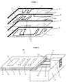
- FIGS 2a and 2b show a second embodiment an anti-intrusion device according to the invention.
- the device 1 consists of three membranes as described previously, A, B and C, glued with double adhesive films face (not shown) on each other. For ease of the representation, these membranes are exaggeratedly spaced on the figures.
- Each membrane has a conductive track 2 on its lower face. These tracks are interconnected by conductive inter-membrane bridges 6, made by means of holes through 4B and 4C through layers B and C and filled with conductive ink composed for example of particles silver taken in a polymer substrate; the whole form thus a conductive barrier in three dimensions. A break at any point this electrical barrier is detected by the device 5.
- the spacing between the different meshes conductive is chosen to minimize the intrusions.
- This device 1 will be applied to the device to be protected from the same way than previously.
- Figure 2a shows a first possible form of the conductive barrier which is a single and continuous track between terminals 2a and 2b occupying the three membranes A, B and C.
- This conductive track can only take two states, "Open” or “closed” between its two terminals, and it will be easy to know the state.
- Figure 2b shows a second possible form of the anti-intrusion conductive barrier. This forms a grid in three dimensions. Its electrical representation can to resemble a mounting of resistors in parallel. Thus, cuts in this grid will result in smaller variations in the case shown in Figure 2a that the person skilled in the art will know how to distinguish from other slight variations like those due to the temperature for example.
- Such a three-dimensional anti-intrusion device is advantageous because it makes the probability even lower of pass through the electrical barrier without being detected, even by cutting with a small tool. Moreover, he makes the intrusion by peeling impossible since it is impossible to peel more than one layer without cutting bridges 6 and be detected.
- FIG. 3 represents in section the combination of a keypad for entering confidential code as well as a display with a security device according to the present invention.
- Four membranes A, B, C and D are fixed on each other.
- the first membrane A comprises on its upper face a drawing 8 indicating the position of the keys on the keyboard. It includes a opening 10 located above the display 7.
- the membranes A, B and D include on their underside a screenprinted track 2 with conductive ink. 4B openings made in the membrane B allow to connect the anti-intrusion tracks 2 of each of the two membranes A and B using traversing bridges 6. For the sake of simplicity, the layers of glue and / or insulating varnish are not shown.
- Conductive tracks 2 of the membranes A and B will be placed above the contacts 9 described below so as to protect them.
- Membranes C and D respectively have on their lower faces and upper conductive elements 9 and spacers 11 so as to form electrical switches allowing to perform the function of keyboard keys according to a known technique, and described in particular in the patent application EP0727796.
- the membrane D also serves as a support for the display 7; it will eventually be covered by a window (not shown) inserted into the openings 10 of membranes A, B and C.
- the anti-intrusion conductive tracks 2 are arranged at immediate vicinity of these openings 10 to avoid any intrusion in this location.
- the conductive track 2 placed on the face lower diaphragm D is connected by conductive bridges 6, passing through conductive bridges 4C and 4D, to tracks 2 of upper membranes.
- the set of tracks 2 present on the lower faces of membranes A, B and D and bridges 6 forms a three-dimensional anti-intrusion conductive barrier, protecting the keyboard and display parts against attacks from all directions.
- This barrier possesses electrical characteristics that will be measured constantly from its terminals 2a and 2b by means 5 (not shown) as previously described.
- FIGS. An advantage of the invention, illustrated in FIGS. comes from the fact that it is possible to integrate within the multilayer structure, and therefore inside the intruder barrier electronic components such as a keyboard, switches, processors, displays ... This allows achieve low cost all kinds of electronic functions completely protected against intrusions from any direction.
- the use of flexible membranes of low Thickness allows easy integration into any device.
- FIG. 5 represents a device 20 for capturing identification code (PIN code) fully secured with the device of the invention as described in FIGS.
- the keyboard and the display are linked to microprocessor 5 by conductive circuits 12 and 13 (represented schematically) grouped in tablecloths and protected against frauds by leads 2 (not represented here by simplicity) until connected to the microprocessor 5.
- the connection of the web (comprising the connections 2a, 2b, 12 and 13) to the microprocessor 5 is embedded in the resin 14 to ensure its inaccessibility.
- This identification code entry device is completely secure since it includes a keyboard, a display and a microprocessor totally dedicated and protected against fraud.
- This device also has the advantages of being manufactured at low cost and represent a small footprint.
- FIG. 6 shows schematically, to facilitate explanation of the different functions, the implementation of a device 20 of the above type on a laptop 30, of to add a fully card payment feature secure.
- the laptop 30 has on its face superior 31 a keyboard 32 and a display 33. It can be worn with a removable handle 34 and communicates with the outside by a serial link with a suitable connector 35 allowing exchanges between its processor 36 and the outside. It is added a card reader, integrated in a compartment autonomous 37, watertight relative to the rest of the apparatus. the figure, a smart card 38 is inserted in the reading position through slot 39 of the card reader.
- a device 20 such as described in Figure 5 is glued on the underside 40 of the device, so as to present a second keyboard 8 and display 7 for entering the PIN code.
- the device 20, placed on the underside, is protected in the usual modes of use of the computer 30 by a removable cover 41.
- the apparatus 30 is turned over and rests on support points protuberances 42 provided on the usually upper face 31 when used as a payment terminal.
- the device 20 enters the compartment 37 through a opening 43 and the electrical connection layer, comprising the connections related to the operation of the keyboard, the display and anti-intrusion trellis, is connected to the inputs of the microprocessor 5 which will manage the payment function. This last is able to detect an intrusion through the device 20 and react to this intrusion.
- a second membrane anti-intrusion 1 as described in Figure 2a is used to protect the upper part of the device, at the compartment 37. It is fixed to the apparatus 30 by gluing on the surface 31.
- An additional diet (no shown) is placed in the protected area, in the resin 14, to make the anti-intrusion device autonomous and functional in case of neutralization of the main power supply of 30.
- an extra security measure it will be possible to provide a device as described in the patent application WO00 / 01100 to avoid the possibility of recovering data confidential from the external power supply of the microprocessor 5.
- One of the advantages of the device 20 according to the invention is its supple and fine membrane structure which facilitates its placement on all kinds of surface.
- the placement of the keyboard and the display for the payment on the back of the device avoids enlarging or cluttering the front surface; the virgin surface is exploited at best. This will in the sense of miniaturization of the devices.
- Another advantage of the device 20 comes from the fact it can be added to a device without compromising its seal, as illustrated in the previous example ( Figure 6).
- FIG. 7a shows the switch 44 in the case of a device in normal operating configuration.
- the device anti-intrusion 1 included between the hood 45 and the surface upper 31 of the device contains a tab 47 placed between two membranes A and B of the device 1, so as to isolate two contacts 48 placed opposite each membrane A and B.
- tongue 47 was attached to the hood 45 and the surface 31 by harpoons 49.
- this switch besides the fact that combines with the security device according to the invention, present many advantages: it is purely mechanical, it is open in normal operation, which avoids wear and tear the oxidation of the contacts for example, it is manufactured at low cost and it is not bulky.
- FIG. 8a shows a smart card 50 in perspective having an anti-intrusion device according to the invention.
- This device according to the invention as described above allows in particular to protect the connection between the chip (not shown) and contacts 51.
- an advantage of the invention is to be able to add to the smart card 50 new features totally secure against fraud as a 52 and a keyboard 53.
- the chip will perform the function of means of measurement. 5.
- a source of energy may be provided for the these new functions.
- Figure 8b shows a smart card incorporating a device according to the invention in section. Unlike the figure 8a, this is a contactless smart card, having a antenna 55. In order not to interfere with the antenna, the intrusion barrier 2 is only used on part of the card out of the antenna, so as to protect the chip 54, a display 7 and a keyboard 9. We can also imagine a keyboard in the antenna field, which would include means such as described in the application FR2736451 to avoid interference between the keyboard and the antenna.
- the safety device occupies all or part of the thickness and the surface a smart card. It is preferably implemented at the card manufacturing. However, it can also be added by the continuation on a classic card so as to cover the card to protect it. For conventional smart cards with contact, used as phone cards, it can be used to protect chip against intrusions to avoid many frauds which involves connecting unwanted chips to the chip initial, in the thickness of the map in an undetectable way to the naked eye.
- FIG. 9 represents a safe 60 incorporating a anti-intrusion device 1 according to the present invention. Its wall has a first thickness 61 steel then a second 62 in hard resin. In the latter is placed an envelope anti-intrusion 1 according to the present invention, covering the entire outer surface of the safe 60.
- the door 63 opens to using a PIN typed on a multilayer keypad protected by a device according to the invention such as that shown in Figure 3.
- a microprocessor 5, arranged inside the safe detects any intrusion through the membranes Anti-intrusion.
- the conductive tracks on the membranes have been performed on the lower faces thereof; they can the same on the upper faces. Only one membrane can have a conductive track 2 on each of its two faces, and have or not bridges 6 to connect these two tracks.
- the device can be made using layers very fine: 0.08 mm, or less if necessary. He can thus occupy a very small location and be very flexible. He can too be thicker if strength and rigidity are needed. It is possible to use various materials according to the report quality / price sought. For example, polyester films, polyurethane.
- the conductive ink used may be based on polymers containing conductive particles of metal (silver, gold) or carbon.
- Such circuits 2 can be made with substrates in Kapton with golden slopes. This last technology possesses, although more expensive excellent features electronic and mechanical.
- the security device can also base its detection deterioration of the tracks, on other electrical characteristics as resistance, for example capacity variations.
- Such a device can be combined with any input system identification, whether entering a PIN code as we have seen it but also the seizure of a biometric imprint, a optical or vocal input, etc.
Landscapes
- Engineering & Computer Science (AREA)
- Computer Hardware Design (AREA)
- Theoretical Computer Science (AREA)
- General Physics & Mathematics (AREA)
- General Engineering & Computer Science (AREA)
- Physics & Mathematics (AREA)
- Microelectronics & Electronic Packaging (AREA)
- Computer Security & Cryptography (AREA)
- Software Systems (AREA)
- Push-Button Switches (AREA)
- Battery Mounting, Suspending (AREA)
- Storage Device Security (AREA)
- Burglar Alarm Systems (AREA)
- Organic Low-Molecular-Weight Compounds And Preparation Thereof (AREA)
- Devices For Checking Fares Or Tickets At Control Points (AREA)
- Window Of Vehicle (AREA)
- Non-Metallic Protective Coatings For Printed Circuits (AREA)
Claims (13)
- Anti-Eindringvorrichtung (1), die Folgendes aufweist: eine leitende Schaltung (2), die auf eine zu schützende Oberfläche platziert wird, die selbst auf einem zu schützenden Element angeordnet ist, und Mittel (5) zum Messen einer elektrischen Charakteristik, die mit der leitenden Schaltung assoziiert ist, und die in der Lage ist zu reagieren im Fall von Modifikationen der elektrischen Charakteristik, wobei die leitende Schaltung (2) teilweise oder vollständig auf einer flexiblen Membran angelegt ist, die auf der zu schützenden Oberfläche fixiert werden soll, dadurch gekennzeichnet, dass sie Kontakte (48) und eine Isolierzunge (47) aufweist, die an einem ihrer Enden fest an dem zu schützenden Element befestigt ist, und deren anderes Ende zwei Positionen einnehmen kann, wobei die erste zwischen den Kontakten (48) und die zweite außerhalb der Kontakte (48) liegt, um einen Schalter (44) zu bilden, der in der Lage ist, die Trennung der Anti-Eindringvorrichtung und des zu schützenden Elements zu detektieren.
- Anti-Eindringvorrichtung nach Anspruch 1, dadurch gekennzeichnet, dass die leitende Schaltung (2) mit leitender Tinte ausgebildet ist.
- Anti-Eindringvorrichtung nach Anspruch 1, dadurch gekennzeichnet, dass die leitende Schaltung (2) ein erstes leitendes Schaltungselement aufweist, das auf die zu schützende Oberfläche platziert ist, und ein zweites leitendes Schaltungselement, das über dem ersten Element platziert ist, und davon durch eine isolierende Schicht getrennt ist, die mit einer leitenden Brücke (6) versehen ist, die die zwei leitenden Schaltungselemente elektrisch verbindet.
- Anti-Eindringvorrichtung nach den Ansprüchen 1 und 3, dadurch gekennzeichnet, dass die Anti-Eindringvorrichtung zwei flexible Membranen aufweist, die unbewegbar aneinander befestigt sind, wobei jede ein leitendes Schaltungselement (2) auf einer ihrer Oberflächen besitzt, und eine leitende Brücke (6) zum Herstellen einer elektrischen Verbindung zwischen den Schaltungselementen jeder der zwei Membranen.
- Anti-Eindringvorrichtung nach Anspruch 4, dadurch gekennzeichnet, dass die Anti-Eindringvorrichtung aus mehreren flexiblen Membranen mit geringer Dicke ausgebildet ist, welche im Siebdruckverfahren hergestellte leitende Membranen aufweisen, die durch leitende Brücken (6) miteinander verbunden sind, die durch die Membrane hindurch ausgebildet sind, um den Eindruck einer einzelnen flexiblen Membran vorzusehen, die eine dreidimensionale Anti-Eindringleitbarriere besitzt.
- Anti-Eindringvorrichtung nach einem der vorhergehenden Ansprüche, dadurch gekennzeichnet, dass die Mittel (5) zum Messen einer elektrischen Charakteristik innerhalb eines Volumens platziert sind, das wenigstens teilweise durch die leitende Schaltung (2) geschützt ist.
- Anti-Eindringvorrichtung nach einem der vorhergehenden Ansprüche, dadurch gekennzeichnet, dass sie eine elektrische Energieversorgung aufweist, die innerhalb eines wenigstens teilweise durch die leitende Schaltung (2) geschützten Volumens platziert ist.
- Anti-Eindringvorrichtung nach Anspruch 4 oder 5, dadurch gekennzeichnet, dass sie eine Komponente, wie beispielsweise einen Schalter (9), eine Anzeige (7) oder einen Mikroprozessor (54) zwischen zwei flexiblen Membranen aufweist.
- Anti-Eindringvorrichtung nach Anspruch 4 oder 5, dadurch gekennzeichnet, dass sie Identifikationseingabemittel (9) und eine Anzeige (7) aufweist, die durch eine leitende Schutzbarriere geschützt sind, und die mit Mitteln verbunden sind zum Durchführen bzw. Managen der Identitätsüberprüfungsfunktionen, innerhalb eines geschützten Volumens.
- Anti-Eindringvorrichtung nach Anspruch 9, die auf einer Vorrichtung (30) platziert ist, dadurch gekennzeichnet, dass die Identifikationseingabemittel (9) an der Unterseite (40) der Einrichtung (30) platziert sind.
- Eine Smart-Card, dadurch gekennzeichnet, dass sie die Vorrichtung nach einem der Ansprüche 1 bis 5 aufweist.
- Ein Safe, dadurch gekennzeichnet, dass er die Einrichtung nach einem der Ansprüche 1 bis 5 aufweist.
- Eine Geheimcode-Eingabevorrichtung, die das Anti-Eindringsystem nach Anspruch 5 aufweist, dadurch gekennzeichnet, dass sie Folgendes aufweist: eine erste Membran mit einer ersten leitenden Anti-Eindringbahn, eine zweite Membran, die eine zweite leitende Eindringbahn aufweist, die elektrisch mit der ersten Anti-Eindringbahn über eine leitende Brücke (6) verbunden ist, eine Membrantastatur deren Kontakte in dem geschützten Bereich zwischen den leitenden Anti-Eindringbahnen platziert sind.
Applications Claiming Priority (2)
| Application Number | Priority Date | Filing Date | Title |
|---|---|---|---|
| FR0001840A FR2805074B1 (fr) | 2000-02-15 | 2000-02-15 | Dispositif anti-intrusion |
| FR0001840 | 2000-02-15 |
Publications (2)
| Publication Number | Publication Date |
|---|---|
| EP1126358A1 EP1126358A1 (de) | 2001-08-22 |
| EP1126358B1 true EP1126358B1 (de) | 2005-04-06 |
Family
ID=8846998
Family Applications (1)
| Application Number | Title | Priority Date | Filing Date |
|---|---|---|---|
| EP01410019A Expired - Lifetime EP1126358B1 (de) | 2000-02-15 | 2001-02-15 | Einbruchhemmende Vorrichtung |
Country Status (4)
| Country | Link |
|---|---|
| EP (1) | EP1126358B1 (de) |
| AT (1) | ATE292817T1 (de) |
| DE (1) | DE60109836T8 (de) |
| FR (1) | FR2805074B1 (de) |
Families Citing this family (19)
| Publication number | Priority date | Publication date | Assignee | Title |
|---|---|---|---|---|
| DE602004013357D1 (de) * | 2003-10-24 | 2008-06-05 | Verifone Systems Ireland Ltd | Schaltungs-sicherheit |
| US8156343B2 (en) | 2003-11-26 | 2012-04-10 | Intel Corporation | Accessing private data about the state of a data processing machine from storage that is publicly accessible |
| US7274289B2 (en) * | 2004-05-27 | 2007-09-25 | Eastman Kodak Company | System and device for detecting object tampering |
| FR2889756B1 (fr) * | 2005-08-11 | 2007-10-12 | Itt Mfg Enterprises Inc | Agencement de securite contre la fraude pour connecteur electrique pour carte a puce |
| DE102005062800A1 (de) | 2005-12-28 | 2007-07-12 | El-Me Ag | Elektronik-Sicherheits-Modul |
| DE102005062799A1 (de) | 2005-12-28 | 2007-07-12 | El-Me Ag | Elektronik-Sicherheits-Modul |
| DE102005062802A1 (de) | 2005-12-28 | 2007-07-12 | El-Me Ag | Elektronik-Sicherheits-Modul |
| ITFI20060077A1 (it) | 2006-03-23 | 2007-09-24 | Gilbarco S P A | Dispositivo per la verifica della regolarita' del funzionamento di terminali automatici di pagamento |
| EP1873680A1 (de) * | 2006-06-23 | 2008-01-02 | ddm hopt + schuler GmbH & Co. KG. | Manipulationsgeschützter Kartenleser |
| FR2906062B1 (fr) | 2006-09-15 | 2010-01-15 | Thales Sa | Systeme anti-intrusion pour la protection de composants electroniques. |
| FR2908544B1 (fr) | 2006-11-10 | 2010-04-09 | Sagem Monetel | Dispositif anti-intrusion |
| DE102007044602A1 (de) * | 2007-09-19 | 2009-04-23 | Continental Automotive Gmbh | Multilayer-Leiterplatte und Verwendung einer Multilayer-Leiterplatte |
| DE102008005442B4 (de) * | 2008-01-22 | 2011-09-22 | Demmel Ag | Manipulationsgeschützte Tastatur |
| WO2010111655A1 (en) | 2009-03-26 | 2010-09-30 | Hypercom Corporation | Keypad membrane security |
| DE102010012851A1 (de) * | 2010-03-25 | 2011-09-29 | Ssp Europe Gmbh | Erfassungseinrichtung zur Erfassung eines Zugriffs durch Unbefugte auf eine Informationstechnikanlage, flüchtige Speichereinrichtung, Schutzvorrichtung, Schutzverfahren sowie Schutzsystem |
| JP2012053788A (ja) * | 2010-09-02 | 2012-03-15 | Canon Inc | 半導体集積回路装置 |
| FR3046480B1 (fr) * | 2015-12-31 | 2018-10-26 | Thales | Systeme de detection d'intrusions |
| CN106022174A (zh) * | 2016-06-24 | 2016-10-12 | 福建睿矽微电子科技有限公司 | 一种安全设备及破坏检测方法 |
| DE102016124335B4 (de) * | 2016-12-14 | 2022-08-18 | Ihp Gmbh - Innovations For High Performance Microelectronics/Leibniz-Institut Für Innovative Mikroelektronik | Manipulationssichere Einhausung von PCBs |
Family Cites Families (4)
| Publication number | Priority date | Publication date | Assignee | Title |
|---|---|---|---|---|
| DE9105960U1 (de) * | 1991-05-14 | 1992-06-11 | Siemens Nixdorf Informationssysteme AG, 4790 Paderborn | Schutzvorrichtung für Schaltungsteile und/oder Daten in einem Gerät zur Authentifikation und Betragsbestätigung |
| GB2270785B (en) * | 1992-09-22 | 1996-05-08 | Gore & Ass | Improvements in security enclosure manufacture |
| GB2297540B (en) * | 1993-03-12 | 1997-01-29 | Gore & Ass | Tamper respondent enclosure |
| DE19705518C2 (de) * | 1997-02-13 | 1999-04-15 | Siemens Ag | Manipulationsgeschütztes elektrisches Gerät |
-
2000
- 2000-02-15 FR FR0001840A patent/FR2805074B1/fr not_active Expired - Fee Related
-
2001
- 2001-02-15 EP EP01410019A patent/EP1126358B1/de not_active Expired - Lifetime
- 2001-02-15 AT AT01410019T patent/ATE292817T1/de not_active IP Right Cessation
- 2001-02-15 DE DE60109836T patent/DE60109836T8/de active Active
Also Published As
| Publication number | Publication date |
|---|---|
| DE60109836D1 (de) | 2005-05-12 |
| ATE292817T1 (de) | 2005-04-15 |
| FR2805074A1 (fr) | 2001-08-17 |
| EP1126358A1 (de) | 2001-08-22 |
| DE60109836T8 (de) | 2006-04-27 |
| FR2805074B1 (fr) | 2003-06-27 |
| DE60109836T2 (de) | 2006-01-12 |
Similar Documents
| Publication | Publication Date | Title |
|---|---|---|
| EP1126358B1 (de) | Einbruchhemmende Vorrichtung | |
| EP2194491B1 (de) | Elektronische Karte, die Steuermittel umfasst | |
| US6929900B2 (en) | Tamper-responding encapsulated enclosure having flexible protective mesh structure | |
| CA2360359C (fr) | Carte a puce sans contact ou hybride contact - sans contact permettant de limiter les risques de fraude | |
| CA2654060C (fr) | Dispositif de protection contre les intrusions d'appareils electroniques | |
| EP0845755B1 (de) | IC-Karte und Program für IC-Karten | |
| EP2146562B1 (de) | Schutzvorrichtung einer elektronischen Komponente | |
| CH619310A5 (en) | Portable card for signal processing system and method of manufacturing this card | |
| FR2604272A1 (fr) | Dispositif de surete pour donnees confidentielles | |
| FR2888975A1 (fr) | Procede de securisation pour la protection de donnees | |
| FR2587816A1 (fr) | Dispositif de securite pour la protection de donnees confidentielles memorisees | |
| EP1116179B1 (de) | Kontaktlose chipkarte mit hemmungsmitteln | |
| US20170185805A1 (en) | Intrusion-protected memory component | |
| EP0231549A1 (de) | Geschützte Umfassung mit elektrischem Schalter und ihre Anwendung | |
| FR2985153A1 (fr) | Dispositif de protection d'un circuit imprime electronique. | |
| US10678958B2 (en) | Intrusion-protected memory component | |
| WO2017077006A1 (fr) | Corps de lecteur de carte à mémoire à treillis de protection recto-verso | |
| EP3291655B1 (de) | Flexible schaltung, und entsprechendes gesichertes anschlussverfahren | |
| EP2102832B1 (de) | Gesichertes gehäuse | |
| CN111868729B (zh) | 受到入侵保护的存储组件 | |
| EP3244377B1 (de) | Wasserdichtes gerät für chipkarten | |
| FR3045889A1 (fr) | Carte a puce du type a bouton poussoir et a batterie et un procede pour sa fabrication | |
| EP3096260A1 (de) | Gesicherte kompakttastatur | |
| CH700045A2 (fr) | Carte electronique ayant des moyens de commande. | |
| EP0665511B1 (de) | Verfahren zum Schützen von Kontaktflächen einer Speicherkarte |
Legal Events
| Date | Code | Title | Description |
|---|---|---|---|
| PUAI | Public reference made under article 153(3) epc to a published international application that has entered the european phase |
Free format text: ORIGINAL CODE: 0009012 |
|
| AK | Designated contracting states |
Kind code of ref document: A1 Designated state(s): AT BE CH CY DE DK ES FI FR GB GR IE IT LI LU MC NL PT SE TR |
|
| AX | Request for extension of the european patent |
Free format text: AL;LT;LV;MK;RO;SI |
|
| 17P | Request for examination filed |
Effective date: 20020221 |
|
| AKX | Designation fees paid |
Free format text: AT BE CH CY DE DK ES FI FR GB GR IE IT LI LU MC NL PT SE TR |
|
| 17Q | First examination report despatched |
Effective date: 20040212 |
|
| GRAP | Despatch of communication of intention to grant a patent |
Free format text: ORIGINAL CODE: EPIDOSNIGR1 |
|
| GRAS | Grant fee paid |
Free format text: ORIGINAL CODE: EPIDOSNIGR3 |
|
| GRAA | (expected) grant |
Free format text: ORIGINAL CODE: 0009210 |
|
| AK | Designated contracting states |
Kind code of ref document: B1 Designated state(s): AT BE CH CY DE DK ES FI FR GB GR IE IT LI LU MC NL PT SE TR |
|
| PG25 | Lapsed in a contracting state [announced via postgrant information from national office to epo] |
Ref country code: IT Free format text: LAPSE BECAUSE OF FAILURE TO SUBMIT A TRANSLATION OF THE DESCRIPTION OR TO PAY THE FEE WITHIN THE PRESCRIBED TIME-LIMIT;WARNING: LAPSES OF ITALIAN PATENTS WITH EFFECTIVE DATE BEFORE 2007 MAY HAVE OCCURRED AT ANY TIME BEFORE 2007. THE CORRECT EFFECTIVE DATE MAY BE DIFFERENT FROM THE ONE RECORDED. Effective date: 20050406 Ref country code: AT Free format text: LAPSE BECAUSE OF FAILURE TO SUBMIT A TRANSLATION OF THE DESCRIPTION OR TO PAY THE FEE WITHIN THE PRESCRIBED TIME-LIMIT Effective date: 20050406 Ref country code: NL Free format text: LAPSE BECAUSE OF FAILURE TO SUBMIT A TRANSLATION OF THE DESCRIPTION OR TO PAY THE FEE WITHIN THE PRESCRIBED TIME-LIMIT Effective date: 20050406 Ref country code: IE Free format text: LAPSE BECAUSE OF FAILURE TO SUBMIT A TRANSLATION OF THE DESCRIPTION OR TO PAY THE FEE WITHIN THE PRESCRIBED TIME-LIMIT Effective date: 20050406 Ref country code: FI Free format text: LAPSE BECAUSE OF FAILURE TO SUBMIT A TRANSLATION OF THE DESCRIPTION OR TO PAY THE FEE WITHIN THE PRESCRIBED TIME-LIMIT Effective date: 20050406 |
|
| REG | Reference to a national code |
Ref country code: GB Ref legal event code: FG4D Free format text: NOT ENGLISH |
|
| REG | Reference to a national code |
Ref country code: CH Ref legal event code: EP |
|
| REG | Reference to a national code |
Ref country code: IE Ref legal event code: FG4D Free format text: LANGUAGE OF EP DOCUMENT: FRENCH |
|
| REF | Corresponds to: |
Ref document number: 60109836 Country of ref document: DE Date of ref document: 20050512 Kind code of ref document: P |
|
| PG25 | Lapsed in a contracting state [announced via postgrant information from national office to epo] |
Ref country code: DK Free format text: LAPSE BECAUSE OF FAILURE TO SUBMIT A TRANSLATION OF THE DESCRIPTION OR TO PAY THE FEE WITHIN THE PRESCRIBED TIME-LIMIT Effective date: 20050706 Ref country code: GR Free format text: LAPSE BECAUSE OF FAILURE TO SUBMIT A TRANSLATION OF THE DESCRIPTION OR TO PAY THE FEE WITHIN THE PRESCRIBED TIME-LIMIT Effective date: 20050706 Ref country code: SE Free format text: LAPSE BECAUSE OF FAILURE TO SUBMIT A TRANSLATION OF THE DESCRIPTION OR TO PAY THE FEE WITHIN THE PRESCRIBED TIME-LIMIT Effective date: 20050706 |
|
| GBT | Gb: translation of ep patent filed (gb section 77(6)(a)/1977) |
Effective date: 20050708 |
|
| PG25 | Lapsed in a contracting state [announced via postgrant information from national office to epo] |
Ref country code: PT Free format text: LAPSE BECAUSE OF FAILURE TO SUBMIT A TRANSLATION OF THE DESCRIPTION OR TO PAY THE FEE WITHIN THE PRESCRIBED TIME-LIMIT Effective date: 20050908 |
|
| NLV1 | Nl: lapsed or annulled due to failure to fulfill the requirements of art. 29p and 29m of the patents act | ||
| REG | Reference to a national code |
Ref country code: IE Ref legal event code: FD4D |
|
| PLBE | No opposition filed within time limit |
Free format text: ORIGINAL CODE: 0009261 |
|
| STAA | Information on the status of an ep patent application or granted ep patent |
Free format text: STATUS: NO OPPOSITION FILED WITHIN TIME LIMIT |
|
| PG25 | Lapsed in a contracting state [announced via postgrant information from national office to epo] |
Ref country code: LI Free format text: LAPSE BECAUSE OF NON-PAYMENT OF DUE FEES Effective date: 20060228 Ref country code: LU Free format text: LAPSE BECAUSE OF NON-PAYMENT OF DUE FEES Effective date: 20060228 Ref country code: CH Free format text: LAPSE BECAUSE OF NON-PAYMENT OF DUE FEES Effective date: 20060228 Ref country code: MC Free format text: LAPSE BECAUSE OF NON-PAYMENT OF DUE FEES Effective date: 20060228 |
|
| 26N | No opposition filed |
Effective date: 20060110 |
|
| REG | Reference to a national code |
Ref country code: CH Ref legal event code: PL |
|
| PG25 | Lapsed in a contracting state [announced via postgrant information from national office to epo] |
Ref country code: TR Free format text: LAPSE BECAUSE OF FAILURE TO SUBMIT A TRANSLATION OF THE DESCRIPTION OR TO PAY THE FEE WITHIN THE PRESCRIBED TIME-LIMIT Effective date: 20050406 |
|
| PG25 | Lapsed in a contracting state [announced via postgrant information from national office to epo] |
Ref country code: CY Free format text: LAPSE BECAUSE OF FAILURE TO SUBMIT A TRANSLATION OF THE DESCRIPTION OR TO PAY THE FEE WITHIN THE PRESCRIBED TIME-LIMIT Effective date: 20050406 |
|
| PG25 | Lapsed in a contracting state [announced via postgrant information from national office to epo] |
Ref country code: ES Free format text: LAPSE BECAUSE OF NON-PAYMENT OF DUE FEES Effective date: 20060228 |
|
| BECA | Be: change of holder's address |
Owner name: INGENICO FRANCE192, AVENUE CHARLES DE GAULLE, F-92 Effective date: 20090806 |
|
| BECN | Be: change of holder's name |
Owner name: INGENICO FRANCE192, AVENUE CHARLES DE GAULLE, F-92 Effective date: 20090806 Owner name: INGENICO FRANCE Effective date: 20090806 |
|
| REG | Reference to a national code |
Ref country code: FR Ref legal event code: TP Ref country code: FR Ref legal event code: CD Ref country code: FR Ref legal event code: CA |
|
| REG | Reference to a national code |
Ref country code: FR Ref legal event code: PLFP Year of fee payment: 15 |
|
| REG | Reference to a national code |
Ref country code: FR Ref legal event code: TP Owner name: COMPAGNIE INDUSTRIELLE ET FINANCIERE D'INGENIE, FR Effective date: 20160111 |
|
| REG | Reference to a national code |
Ref country code: FR Ref legal event code: PLFP Year of fee payment: 16 |
|
| REG | Reference to a national code |
Ref country code: FR Ref legal event code: CA Effective date: 20160304 Ref country code: FR Ref legal event code: CD Owner name: INGENICO GROUP, FR Effective date: 20160304 |
|
| REG | Reference to a national code |
Ref country code: FR Ref legal event code: PLFP Year of fee payment: 17 |
|
| PGFP | Annual fee paid to national office [announced via postgrant information from national office to epo] |
Ref country code: BE Payment date: 20170223 Year of fee payment: 17 |
|
| REG | Reference to a national code |
Ref country code: FR Ref legal event code: PLFP Year of fee payment: 18 |
|
| REG | Reference to a national code |
Ref country code: BE Ref legal event code: MM Effective date: 20180228 |
|
| PG25 | Lapsed in a contracting state [announced via postgrant information from national office to epo] |
Ref country code: BE Free format text: LAPSE BECAUSE OF NON-PAYMENT OF DUE FEES Effective date: 20180228 |
|
| PGFP | Annual fee paid to national office [announced via postgrant information from national office to epo] |
Ref country code: DE Payment date: 20200211 Year of fee payment: 20 Ref country code: GB Payment date: 20200219 Year of fee payment: 20 |
|
| PGFP | Annual fee paid to national office [announced via postgrant information from national office to epo] |
Ref country code: FR Payment date: 20200214 Year of fee payment: 20 |
|
| REG | Reference to a national code |
Ref country code: DE Ref legal event code: R071 Ref document number: 60109836 Country of ref document: DE |
|
| REG | Reference to a national code |
Ref country code: GB Ref legal event code: PE20 Expiry date: 20210214 |
|
| PG25 | Lapsed in a contracting state [announced via postgrant information from national office to epo] |
Ref country code: GB Free format text: LAPSE BECAUSE OF EXPIRATION OF PROTECTION Effective date: 20210214 |