EP2194491B1 - Elektronische Karte, die Steuermittel umfasst - Google Patents
Elektronische Karte, die Steuermittel umfasst Download PDFInfo
- Publication number
- EP2194491B1 EP2194491B1 EP09014865A EP09014865A EP2194491B1 EP 2194491 B1 EP2194491 B1 EP 2194491B1 EP 09014865 A EP09014865 A EP 09014865A EP 09014865 A EP09014865 A EP 09014865A EP 2194491 B1 EP2194491 B1 EP 2194491B1
- Authority
- EP
- European Patent Office
- Prior art keywords
- electronic card
- integrated circuit
- insulating layer
- card
- circuit board
- Prior art date
- Legal status (The legal status is an assumption and is not a legal conclusion. Google has not performed a legal analysis and makes no representation as to the accuracy of the status listed.)
- Active
Links
Images

Classifications
-
- G—PHYSICS
- G06—COMPUTING OR CALCULATING; COUNTING
- G06K—GRAPHICAL DATA READING; PRESENTATION OF DATA; RECORD CARRIERS; HANDLING RECORD CARRIERS
- G06K19/00—Record carriers for use with machines and with at least a part designed to carry digital markings
- G06K19/06—Record carriers for use with machines and with at least a part designed to carry digital markings characterised by the kind of the digital marking, e.g. shape, nature, code
- G06K19/067—Record carriers with conductive marks, printed circuits or semiconductor circuit elements, e.g. credit or identity cards also with resonating or responding marks without active components
- G06K19/07—Record carriers with conductive marks, printed circuits or semiconductor circuit elements, e.g. credit or identity cards also with resonating or responding marks without active components with integrated circuit chips
- G06K19/0716—Record carriers with conductive marks, printed circuits or semiconductor circuit elements, e.g. credit or identity cards also with resonating or responding marks without active components with integrated circuit chips at least one of the integrated circuit chips comprising a sensor or an interface to a sensor
-
- G—PHYSICS
- G06—COMPUTING OR CALCULATING; COUNTING
- G06F—ELECTRIC DIGITAL DATA PROCESSING
- G06F3/00—Input arrangements for transferring data to be processed into a form capable of being handled by the computer; Output arrangements for transferring data from processing unit to output unit, e.g. interface arrangements
- G06F3/01—Input arrangements or combined input and output arrangements for interaction between user and computer
- G06F3/03—Arrangements for converting the position or the displacement of a member into a coded form
- G06F3/041—Digitisers, e.g. for touch screens or touch pads, characterised by the transducing means
- G06F3/044—Digitisers, e.g. for touch screens or touch pads, characterised by the transducing means by capacitive means
- G06F3/0443—Digitisers, e.g. for touch screens or touch pads, characterised by the transducing means by capacitive means using a single layer of sensing electrodes
Definitions
- the invention relates to an electronic card, such as a smart card, which comprises integrated control means.
- the electronic card comprises at least one integrated circuit arranged, which may be arranged on a printed circuit board, means for connection to a power source for supplying said integrated circuit, and control means operable manually and connected to the circuit. integrated.
- Said integrated circuit is provided mainly for the processing of the signals generated by the control means.
- the integrated circuit, the control means and at least a part of the connection means to the power source are enclosed or encapsulated in at least one layer of an insulating material forming said card.
- An electronic card provided with all electronic components may be of generally rectangular shape. However, this electronic card can also be of another profile, for example of generally circular shape.
- This electronic card such as a smart card, must be of a small thickness, for example less than 2 mm, and preferably close to 0.8 mm.
- Such an electronic card may conventionally be a card of the banking type, in particular according to the ISO standard, but also a card in the form of an electronic device designated Token in English terminology.
- Such an electronic device can be of two types, namely a first type with an integrated precise time base, or a second type, which does not require a precise time base.
- the patent application US 2008/0150905 A1 discloses a computer device, such as a notebook, a PDA device, or a mobile phone, which includes a capacitive touch screen.
- a computer device such as a notebook, a PDA device, or a mobile phone, which includes a capacitive touch screen.
- a parasitic capacitor is produced with at least one ground-connected electrode disposed under the capacitive sensing electrode. The frequency of the oscillator without capacitive detection is based on the parasitic capacitor thus produced.
- the computer device is relatively large size, and most of these components can not be integrated into an electronic card type credit card.
- the control means generally used for the execution of at least one function or the introduction of data or commands are in the form of pushbuttons defining dome portions on the outer surface of the card.
- the object of the invention is therefore to provide an electronic card which comprises control means for executing certain functions or for the introduction of at least one data item or command, while having a thin and ensuring good operating reliability to overcome the disadvantages of the state of the art cited above.
- An advantage of the electronic card according to the invention lies in the fact that the control means in the form of electrodes capacitive keys, occupy a relatively limited space in the electronic card. With this, it is possible to minimize the thickness of such an electronic card as required.
- a shielding conductive screen is disposed in or on the electronic card.
- This shielding screen is disposed on one side of the electrodes of the capacitive keys, which is opposite to the contact surface.
- This conductive screen is remote and non-contact with the capacitive keys. It can be connected to one of the terminals of the power source.
- the layer of insulating material is fixed directly to the printed circuit board, which may be flexible, for example made of polyimide.
- the layer of insulating material 3 is fed as a resin on one side carrying the electronic elements of the printed circuit board 2.
- This resin may be polyurethane. After a well-known rolling and solidifying operation of this resin, the electronic card with the integrated electronic elements is thus produced with a small thickness of less than 2 mm, and preferably close to 0.76 mm, or even less.
- Other metal wires 17 may be provided for connecting the integrated circuit to a display device explained hereinafter with reference to the Figures 2 to 4 .
- Contact pads of the integrated circuit 5 may be connected to the printed circuit board 2, in particular by a technique called Flip chip in English terminology.
- capacitive key electrodes arranged as the keys of a traditional telephone keypad to define numbers, letters or symbols. In a normal operating mode, a single capacitive key for each action of a user's finger D can be activated and detected by the circuit integrated. However it may be conceivable that two or more adjacent keys may be activated at the same time in the case of a configuration of the integrated circuit to define a computer cursor.
- the processing unit is configured to take into account the distance separating the finger D in contact with the contact surface and the capacitive key to activate. To do this, it is necessary for the distance e1 between said contact surface 20 and the capacitive keys 6 to be less than the thickness e2 of the layer of insulating material 3, which is disposed on a side opposite to said contact surface. As a function of a detection threshold determined in the processing unit of the integrated circuit 5, this processing unit detects only the presence of a finger D in contact on the contact surface. next to at least one of the touch keys to activate.
- the thickness e2 of this layer of insulating material 3 as seen in FIG. Figure 1A can be for example of the order of 0.45 to 0.5 mm, while the thickness e1 of the printed circuit board 2 can be for example of the order of 0.1 to 0.15 mm. Therefore, if the dielectric constant of the layer of insulating material 3, is substantially equivalent to that of the printed circuit board 2, the integrated circuit 5 can be configured to detect only one action of a finger D d a user on the contact surface 20. Of course, in the case where the dielectric constant of the printed circuit board is greater than that of the layer of insulating material 3, the difference in thickness may no longer be essential to detect an action of a finger only on the contact surface.
- the processing unit of the integrated circuit 5 generally comprises a multiplexer, to the input of which are connected all the capacitive keys 6, an oscillator analog block and a measurement and comparison logic block.
- the analog block may include a voltage controlled oscillator, which is connected to the output of the multiplexer.
- the task of the multiplexer is to successively and periodically connect each touch key to the input of the oscillator as a function of control bit words provided by the measurement and comparison logic block.
- the logic block is able to determine a certain number of positions of the finger on said capacitive keys, for example 12 positions.
- an integrated circuit 5 for processing the signals generated by the control means 6 an integrated circuit for a memory unit, an integrated circuit for a microcontroller connected to the other integrated circuits, and possibly a specific drive circuit for controlling a display device, such as an LCD device.
- the microcontroller defined under the reference EM 6819 manufactured by the company EM Microelectronic-Marin SA in Switzerland, can be used in the electronic card.
- the electronic card 1 may further comprise a control member in the form of a switch button not shown.
- This well-known button switch can be activated from outside the card by a user for a specified duration, for example a duration of 5, 10 or 15 seconds so as to control the activation of the control means via the integrated circuit powered by the battery 4. Without action on the capacitive keys after a duration which may be equivalent to that of the activation, said keys are placed in a rest mode.
- the printed circuit board 2 which may be flexible or rigid, comprises on one side, at least one integrated circuit 5 and the electrodes of the capacitive keys 6 of the control means, connected to the integrated circuit .
- the power source 4 which is a battery or battery, is disposed on one side of the printed circuit board 2 and connected to said plate by two metal flanges for supplying the integrated circuit.
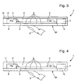
- a display device of the LCD type 7 is provided on one side of the printed circuit board. This display device 7 is connected by a set of tracks or metal wires to the integrated circuit 5, which may include a drive circuit of said display device.
- the display device can be provided above the display device to define a field of view of said device, an opening 13 made in the first insulating layer 3. However, in place of the opening, it can be provided that a portion the display device 7 is visible through at least one transparent portion 13 of the first layer of insulating material 3.
- This screen may be a conductive film, such as a metal film made of nickel or copper or a metal insert.
- This shielding screen 10 is remote and without direct contact with the capacitive keys 6. It can be connected to a terminal of the battery or remain in a floating state. This shielding screen can completely cover the second face of the printed circuit board or at least one area opposite all the capacitive keys 6.
- a grid instead of a solid metal layer can also be provided as shielding screen.
- the layer of insulating material comprises a first insulating layer 3 and a second insulating layer 8.
- the battery 4, the display device 7, the printed circuit board 2, the integrated circuit 5 and the electrodes of the capacitive keys 6 are encapsulated between the first and the second insulating layers.
- the printed circuit board 2 which can be flexible, is double-sided. On a first face, at least one integrated circuit 5 for processing the signals generated by the control means is connected. The connection paths to the device 7 can also be provided on this first face, as well as the connection by means of the two metal flanges at the terminals of the battery 4. On the other hand, all the electrodes of the capacitive keys 6 are arranged on a second face of the plate. printed circuit 2, which is opposite to the first face. Conductive passages, not shown, through the printed circuit board 2 may be provided for connecting the electrodes of the capacitive keys to the integrated circuit.
- An opening 13 may be made in the second insulating layer 8 to view a display portion of the display device 7. However, in place of the opening, it may be provided that a display portion of the display device 7 is visible through at least one transparent portion 13 of the second insulating layer 8.
- the figure 4 represents a cross section of a third embodiment of the electronic card 1 according to the invention. It should be noted that all the same elements of the electronic card 1 described below bear reference signs identical to those of the Figures 1 to 3 . For the sake of simplification, it will not be repeated in detail the description of each element for this figure 4 .
Landscapes
- Engineering & Computer Science (AREA)
- Theoretical Computer Science (AREA)
- Computer Hardware Design (AREA)
- Microelectronics & Electronic Packaging (AREA)
- Physics & Mathematics (AREA)
- General Physics & Mathematics (AREA)
- General Engineering & Computer Science (AREA)
- Human Computer Interaction (AREA)
- Credit Cards Or The Like (AREA)
Claims (15)
- Elektronische Karte (1) in Form einer Bankkarte, die wenigstens eine integrierte Schaltung (5), Mittel zum Verbinden mit einer elektrischen Versorgungsquelle (4) für die Versorgung der integrierten Schaltung und Steuermittel (6), die manuell betätigbar sind und mit der integrierten Schaltung für die Verarbeitung von durch die Steuermittel erzeugten Signalen verbunden sind, umfasst, wobei die integrierte Schaltung, die Steuermittel und wenigstens ein Teil der Mittel für die Verbindung mit der Versorgungsquelle in wenigstens eine Schicht aus einem isolierendem Material (3), das die Karte bildet, eingeschlossen oder eingekapselt sind, wobei die Steuermittel aus einer Gesamtheit von Elektroden (6) gebildet sind, um einen Berührungsschirm mit kapazitiven Tasten zu definieren, die jeweils durch einen Finger (D) eines Anwenders oder durch einen Stift, der auf einer Kontaktoberfläche (20) der Karte gegenüber wenigstens einer berührungsempfindlichen Taste angeordnet wird, aktivierbar sind, um Daten oder einen Befehl einzugeben,
dadurch gekennzeichnet, dass die elektronische Karte eine leitende Abschirmung (10, 11, 12) umfasst, die auf einer Seite der Elektroden der kapazitiven Tasten (6) angeordnet ist, die der Kontaktoberfläche (20) gegenüber liegt, wobei die leitende Abschirmung von den kapazitiven Tasten beabstandet und nicht mit diesen in Kontakt ist. - Elektronische Karte (1) nach Anspruch 1, dadurch gekennzeichnet, dass die integrierte Schaltung (5) auf einer gedruckten Leiterplatte (2) angeordnet ist.
- Elektronische Karte (1) nach Anspruch 2, dadurch gekennzeichnet, dass sie eine Stromversorgungsquelle (4) umfasst, die mit der gedruckten Leiterplatte (2) über Verbindungsmittel verbunden ist.
- Elektronische Karte (1) nach Anspruch 2, dadurch gekennzeichnet, dass sie eine Anzeigevorrichtung (7) umfasst, die mit der integrierten Schaltung (5) oder mit einer mit der integrierten Schaltung verbundenen Treiberschaltung verbunden ist, wobei ein Anzeigeabschnitt der Anzeigevorrichtung durch eine
Öffnung (13) sichtbar ist, die in der Schicht aus Isoliermaterial (3) ausgebildet ist, wobei die Anzeigevorrichtung nicht über oder unter der Gesamtheit der Elektroden der Steuermittel angeordnet ist. - Elektronische Karte (1) nach Anspruch 2, dadurch gekennzeichnet, dass sie eine Anzeigevorrichtung (7) umfasst, die mit der integrierten Schaltung (5) oder mit einer mit der integrierten Schaltung verbundenen Treiberschaltung verbunden ist, wobei ein Anzeigeabschnitt der Anzeigevorrichtung durch wenigstens einen lichtdurchlässigen Teil (13) der Schicht aus Isoliermaterial (3) sichtbar ist, wobei die Anzeigevorrichtung nicht über oder unter der Gesamtheit der Elektroden der Steuermittel angeordnet ist.
- Elektronische Karte (1) nach einem der vorhergehenden Ansprüche, dadurch gekennzeichnet, dass sie ein manuell betätigbares Steuerorgan umfasst, das mit der integrierten Schaltung verbunden ist und die Inbetriebnahme der Berührungstasten und/oder der Anzeigevorrichtung (7) steuern kann.
- Elektronische Karte (1) nach Anspruch 6, dadurch gekennzeichnet, dass das Steuerorgan ein Unterbrechungsschaltknopf ist, der während einer vorgegebenen Dauer manuell gedrückt werden kann, um die berührungsempfindlichen Tasten und/oder die Anzeigevorrichtung in Betrieb zu nehmen.
- Elektronische Karte (1) nach einem der Ansprüche 4 und 5, dadurch gekennzeichnet, dass die Schicht aus Isoliermaterial aus einer ersten Isolierschicht (3) und einer zweiten Isolierschicht (8) gebildet ist, wobei die Versorgungsquelle, die ein Batteriepack (4) ist, die Anzeigevorrichtung (7), die gedruckte Leiterplatte (2), die integrierte Schaltung (5) und die Elektroden der kapazitiven Tasten (6) zwischen der ersten und der zweiten Isolierschicht eingeschlossen oder eingekapselt sind.
- Elektronische Karte (1) nach Anspruch 8, dadurch gekennzeichnet, dass die gedruckte Leiterplatte (2) biegsam und einseitig ist, dass die integrierte Schaltung und die Elektroden der kapazitiven Tasten (6) auf einer ersten Seite der gedruckten Leiterplatte angeordnet sind, indem sie in die erste Isolierschicht (3) eingekapselt sind, wobei sich die Kontaktoberfläche (20) auf der äußeren Oberfläche der ersten Isolierschicht befindet, und dass die Abschirmung durch eine leitende dünne Schicht (10) oder ein leitendes Gitter gebildet ist, die auf der zweiten Oberfläche der gedruckten Leiterplatte gegenüber wenigstens sämtlicher Elektroden der kapazitiven Tasten angeordnet ist und in die Karte durch die zweite Isolierschicht (8), die an der ersten Isolierschicht befestigt ist, eingeschlossen ist.
- Elektronische Karte (1) nach Anspruch 8, dadurch gekennzeichnet, dass die gedruckte Leiterplatte (2) biegsam und doppelseitig ist, dass die integrierte Schaltung (5) auf einer ersten Seite der gedruckten Leiterplatte angeordnet ist, indem sie in die erste Isolierschicht (3) eingekapselt ist, und dass die Elektroden der kapazitiven Tasten (6) auf einer zweiten gegenüberliegenden Seite der gedruckten Leiterplatte angeordnet sind und in die Karte durch die zweite Isolierschicht (8), die an der ersten Isolierschicht befestigt ist, eingeschlossen sind, wobei sich die Kontaktoberfläche (20) auf der äußeren Oberfläche der zweiten Isolierschicht befindet.
- Elektronische Karte (1) nach Anspruch 10, dadurch gekennzeichnet, dass die leitende Abschirmung durch leitende Partikel (11) gebildet ist, die wenigstens in eine bestimmte Dicke der ersten Isolierschicht (3) ausgehend von der äußeren Oberfläche integriert sind, die sich wenigstens über eine Zone gegenüber sämtlichen kapazitiven Tasten (6) erstreckt.
- Elektronische Karte (1) nach Anspruch 10, dadurch gekennzeichnet, dass die leitende Abschirmung durch eine dünne leitende Schicht oder durch eine lichtundurchlässige Farbschicht (12) gebildet ist, die auf der äußeren Oberfläche der ersten Isolierschicht (3) angeordnet ist, wobei sich die leitende dünne Schicht oder die Farbschicht wenigstens über eine Zone gegenüber sämtlichen kapazitiven Tasten (6) erstreckt.
- Elektronische Karte (1) nach einem der vorhergehenden Ansprüche, dadurch gekennzeichnet, dass sie eine Speichereinheit, um persönliche Daten und/oder wenigstens einen persönlichen Identifizierungscode und/oder Konfigurationsparameter zu speichern, und eine Mikrocontroller-Einheit, die mit der Speichereinheit verbunden ist, umfasst und dass sie 12 Elektroden für kapazitive Tasten (6) für die jeweilige Ausführung einer spezifischen Funktion oder für die Eingabe von Daten, die in Verbindung mit der integrierten Schaltung (5) definiert sind, umfasst.
- Elektronische Karte (1) nach Anspruch 1, dadurch gekennzeichnet, dass die leitende Abschirmung (10, 11, 12) in einem schwebenden Zustand ist.
- Elektronische Karte (1) nach Anspruch 1, dadurch gekennzeichnet, dass die Elektroden (6) als Funktion der ungefähren Kontaktoberfläche eines Fingers auf der Kontaktoberfläche bemessen sind und ausreichend voneinander beabstandet sind.
Priority Applications (1)
| Application Number | Priority Date | Filing Date | Title |
|---|---|---|---|
| EP09014865A EP2194491B1 (de) | 2008-12-02 | 2009-12-01 | Elektronische Karte, die Steuermittel umfasst |
Applications Claiming Priority (2)
| Application Number | Priority Date | Filing Date | Title |
|---|---|---|---|
| EP08020862A EP2194489A1 (de) | 2008-12-02 | 2008-12-02 | Elektronische Karte, die Steuermittel umfasst |
| EP09014865A EP2194491B1 (de) | 2008-12-02 | 2009-12-01 | Elektronische Karte, die Steuermittel umfasst |
Publications (2)
| Publication Number | Publication Date |
|---|---|
| EP2194491A1 EP2194491A1 (de) | 2010-06-09 |
| EP2194491B1 true EP2194491B1 (de) | 2012-08-01 |
Family
ID=40453066
Family Applications (2)
| Application Number | Title | Priority Date | Filing Date |
|---|---|---|---|
| EP08020862A Withdrawn EP2194489A1 (de) | 2008-12-02 | 2008-12-02 | Elektronische Karte, die Steuermittel umfasst |
| EP09014865A Active EP2194491B1 (de) | 2008-12-02 | 2009-12-01 | Elektronische Karte, die Steuermittel umfasst |
Family Applications Before (1)
| Application Number | Title | Priority Date | Filing Date |
|---|---|---|---|
| EP08020862A Withdrawn EP2194489A1 (de) | 2008-12-02 | 2008-12-02 | Elektronische Karte, die Steuermittel umfasst |
Country Status (5)
| Country | Link |
|---|---|
| US (1) | US8381992B2 (de) |
| EP (2) | EP2194489A1 (de) |
| CN (1) | CN101751602B (de) |
| CA (1) | CA2686534C (de) |
| TW (1) | TWI455032B (de) |
Families Citing this family (42)
| Publication number | Priority date | Publication date | Assignee | Title |
|---|---|---|---|---|
| KR20120019543A (ko) * | 2010-08-26 | 2012-03-07 | 삼성전자주식회사 | 온-셀 tsp 표시장치 |
| CN107273021A (zh) * | 2010-11-22 | 2017-10-20 | 株式会社Ip舍路信 | 信息输入系统、程序、介质 |
| EP2619968A4 (de) * | 2011-01-28 | 2013-10-09 | Siemens Medical Instr Pte Ltd | Zur fernsteuerung einer elektronischen vorrichtung konfigurierte steuerungsanordnung |
| CN102686012B (zh) | 2011-03-18 | 2017-03-15 | 爱立信(中国)通信有限公司 | 静电屏蔽装置、电子设备及制作该静电屏蔽装置的方法 |
| TWM432086U (en) * | 2011-10-31 | 2012-06-21 | Yi-Ta Chen | Proximity sensing device having keyboard function |
| CN104169850B (zh) | 2012-01-12 | 2017-06-06 | 辛纳普蒂克斯公司 | 单层电容性成像传感器 |
| GB2502088A (en) * | 2012-05-16 | 2013-11-20 | St Microelectronics Res & Dev | Improved remote control |
| US8777115B2 (en) * | 2012-07-13 | 2014-07-15 | Syscard Innovations Inc. | Card switch |
| TWI492163B (zh) * | 2013-02-20 | 2015-07-11 | Smartdisplayer Technology Co Ltd | Electronic card and its capacitive touch sensing method |
| CN104009744B (zh) * | 2013-02-26 | 2017-03-01 | 智慧光科技股份有限公司 | 电子卡及其电容式触碰感应方法 |
| EP2772837A1 (de) * | 2013-02-28 | 2014-09-03 | Nxp B.V. | Berührungssensor für Chipkarten |
| RU2013133076A (ru) * | 2013-07-17 | 2015-01-27 | Андрей Алексеевич Провкин | Устройство и способ аутентификации |
| US9542023B2 (en) | 2013-08-07 | 2017-01-10 | Synaptics Incorporated | Capacitive sensing using matrix electrodes driven by routing traces disposed in a source line layer |
| US20150091842A1 (en) | 2013-09-30 | 2015-04-02 | Synaptics Incorporated | Matrix sensor for image touch sensing |
| US10042489B2 (en) | 2013-09-30 | 2018-08-07 | Synaptics Incorporated | Matrix sensor for image touch sensing |
| US9298325B2 (en) | 2013-09-30 | 2016-03-29 | Synaptics Incorporated | Processing system for a capacitive sensing device |
| US9459367B2 (en) | 2013-10-02 | 2016-10-04 | Synaptics Incorporated | Capacitive sensor driving technique that enables hybrid sensing or equalization |
| US9274662B2 (en) | 2013-10-18 | 2016-03-01 | Synaptics Incorporated | Sensor matrix pad for performing multiple capacitive sensing techniques |
| US9495046B2 (en) | 2013-10-23 | 2016-11-15 | Synaptics Incorporated | Parasitic capacitance filter for single-layer capacitive imaging sensors |
| US9081457B2 (en) | 2013-10-30 | 2015-07-14 | Synaptics Incorporated | Single-layer muti-touch capacitive imaging sensor |
| US9798429B2 (en) | 2014-02-28 | 2017-10-24 | Synaptics Incorporated | Guard electrodes in a sensing stack |
| US10133421B2 (en) | 2014-04-02 | 2018-11-20 | Synaptics Incorporated | Display stackups for matrix sensor |
| EP2933759A1 (de) * | 2014-04-18 | 2015-10-21 | Gemalto SA | Herstellungsverfahren einer Vorrichtung mit elektronischem/elektrischem Schaltkreis |
| US9927832B2 (en) | 2014-04-25 | 2018-03-27 | Synaptics Incorporated | Input device having a reduced border region |
| US9690397B2 (en) | 2014-05-20 | 2017-06-27 | Synaptics Incorporated | System and method for detecting an active pen with a matrix sensor |
| US10175827B2 (en) | 2014-12-23 | 2019-01-08 | Synaptics Incorporated | Detecting an active pen using a capacitive sensing device |
| US9778713B2 (en) | 2015-01-05 | 2017-10-03 | Synaptics Incorporated | Modulating a reference voltage to preform capacitive sensing |
| US9939972B2 (en) | 2015-04-06 | 2018-04-10 | Synaptics Incorporated | Matrix sensor with via routing |
| US9720541B2 (en) | 2015-06-30 | 2017-08-01 | Synaptics Incorporated | Arrangement of sensor pads and display driver pads for input device |
| US9715304B2 (en) | 2015-06-30 | 2017-07-25 | Synaptics Incorporated | Regular via pattern for sensor-based input device |
| US10095948B2 (en) | 2015-06-30 | 2018-10-09 | Synaptics Incorporated | Modulation scheme for fingerprint sensing |
| CN205028263U (zh) | 2015-09-07 | 2016-02-10 | 辛纳普蒂克斯公司 | 一种电容传感器 |
| US10037112B2 (en) | 2015-09-30 | 2018-07-31 | Synaptics Incorporated | Sensing an active device'S transmission using timing interleaved with display updates |
| US10067587B2 (en) | 2015-12-29 | 2018-09-04 | Synaptics Incorporated | Routing conductors in an integrated display device and sensing device |
| CN106933400B (zh) | 2015-12-31 | 2021-10-29 | 辛纳普蒂克斯公司 | 单层传感器图案和感测方法 |
| JPWO2017142093A1 (ja) * | 2016-02-17 | 2019-03-22 | 株式会社I・Pソリューションズ | 装置、及びカード型装置 |
| US9773153B1 (en) * | 2016-03-24 | 2017-09-26 | Fingerprint Cards Ab | Fingerprint sensor module |
| US10282651B2 (en) * | 2017-03-23 | 2019-05-07 | Idex Asa | Sensor array system selectively configurable as a fingerprint sensor or data entry device |
| FR3098371B1 (fr) * | 2019-07-05 | 2021-09-24 | Linxens Holding | Dispositif de connexion de carte a puce sur textile |
| WO2021022625A1 (zh) * | 2019-08-02 | 2021-02-11 | 深圳市越疆科技有限公司 | 装置的避障方法、装置和控制器 |
| CN111524883B (zh) * | 2020-04-29 | 2022-09-20 | 业成科技(成都)有限公司 | 膜内电子组件及其制备方法 |
| US20240185220A1 (en) * | 2022-12-03 | 2024-06-06 | Visa International Service Association | Two payment account numbers in one card |
Family Cites Families (12)
| Publication number | Priority date | Publication date | Assignee | Title |
|---|---|---|---|---|
| US5543588A (en) * | 1992-06-08 | 1996-08-06 | Synaptics, Incorporated | Touch pad driven handheld computing device |
| FR2755269B1 (fr) | 1996-10-25 | 1998-12-04 | Asulab Sa | Dispositif d'identification d'une action manuelle sur une surface, notamment pour une piece d'horlogerie |
| US6091082A (en) * | 1998-02-17 | 2000-07-18 | Stmicroelectronics, Inc. | Electrostatic discharge protection for integrated circuit sensor passivation |
| RU2179337C2 (ru) * | 1999-03-01 | 2002-02-10 | ОПТИВА, Инк. | Смарт-карта (электронная карта) и способ ее изготовления |
| US6816058B2 (en) * | 2001-04-26 | 2004-11-09 | Mcgregor Christopher M | Bio-metric smart card, bio-metric smart card reader and method of use |
| US6641050B2 (en) * | 2001-11-06 | 2003-11-04 | International Business Machines Corporation | Secure credit card |
| US7566001B2 (en) * | 2003-08-29 | 2009-07-28 | Semiconductor Energy Laboratory Co., Ltd. | IC card |
| JP2006134145A (ja) * | 2004-11-08 | 2006-05-25 | Seiko Epson Corp | Icカード |
| JP2009527894A (ja) | 2005-12-14 | 2009-07-30 | コーニンクレッカ フィリップス エレクトロニクス エヌ ヴィ | Ledを変調するための回路配置及びledの動作方法 |
| TWM293556U (en) * | 2005-12-30 | 2006-07-01 | Kanghong Entpr Co Ltd | Plug-in card connector |
| JP2008097283A (ja) * | 2006-10-11 | 2008-04-24 | Hosiden Corp | タッチパネル入力装置 |
| US8120584B2 (en) * | 2006-12-21 | 2012-02-21 | Cypress Semiconductor Corporation | Feedback mechanism for user detection of reference location on a sensing device |
-
2008
- 2008-12-02 EP EP08020862A patent/EP2194489A1/de not_active Withdrawn
-
2009
- 2009-11-27 CA CA2686534A patent/CA2686534C/en active Active
- 2009-11-30 TW TW098140818A patent/TWI455032B/zh active
- 2009-12-01 US US12/628,618 patent/US8381992B2/en active Active
- 2009-12-01 EP EP09014865A patent/EP2194491B1/de active Active
- 2009-12-02 CN CN200910246900.3A patent/CN101751602B/zh not_active Expired - Fee Related
Also Published As
| Publication number | Publication date |
|---|---|
| EP2194491A1 (de) | 2010-06-09 |
| US8381992B2 (en) | 2013-02-26 |
| CA2686534A1 (en) | 2010-06-02 |
| EP2194489A1 (de) | 2010-06-09 |
| US20100140359A1 (en) | 2010-06-10 |
| CN101751602B (zh) | 2014-11-05 |
| CN101751602A (zh) | 2010-06-23 |
| TW201033881A (en) | 2010-09-16 |
| CA2686534C (en) | 2014-12-30 |
| TWI455032B (zh) | 2014-10-01 |
Similar Documents
| Publication | Publication Date | Title |
|---|---|---|
| EP2194491A1 (de) | Elektronische Karte, die Steuermittel umfasst | |
| EP1692642B1 (de) | Sicherheitsdokument mit einem kontaktlosen chip mit datenmaskierung | |
| EP2766769B1 (de) | Anzeigevorrichtung multifunktioneller kommunikationsoberfläche | |
| EP2221755B1 (de) | Chip-Karte mit einem Sensor, und Verfahren zur Herstellung der Chip-Karte | |
| FR3063555A1 (fr) | Carte a puce et procede de fabrication d’une carte a puce | |
| EP2218040A1 (de) | Hochfrequenzkommunikationseinrichtung mit einem timer | |
| EP2128805B1 (de) | Chipkarte mit zusätzlichen elektronischen Mitteln | |
| EP1126358B1 (de) | Einbruchhemmende Vorrichtung | |
| EP1116179B1 (de) | Kontaktlose chipkarte mit hemmungsmitteln | |
| EP3343450B1 (de) | Tragbarer gegenstand, der eine nahfeldverbindungsvorrichtung umfasst | |
| EP2780867A1 (de) | Hochfrequenzkommunikationsvorrichtung mit durch beliebige gesten des trägers gesteuertem betrieb | |
| FR2907563A1 (fr) | Ecran tactile et terminal de paiement comprenant cet ecran. | |
| CH700045A2 (fr) | Carte electronique ayant des moyens de commande. | |
| EP3379389B1 (de) | Gesicherte tastatur für elektronische datenerfassungsvorrichtung | |
| FR2474204A1 (fr) | Dispositif electronique portatif, notamment pour l'identification de son porteur | |
| EP2869243A1 (de) | Chipkarte mit Batterie, und Herstellungsverfahren einer solchen Karte | |
| WO2008080812A9 (fr) | Module de commande electrique, en particulier pour vehicule automobile | |
| EP1158375A1 (de) | Elektronische Vorrichtung zum Ausarbeiten und Anzeigen von Informationen | |
| FR2908552A1 (fr) | Interrupteur de circuit electronique protege contre un acces exterieur | |
| EP1808751A1 (de) | Elektronische Vorrichtung zur Betätigung von Berührungstasten, die eine Cursorfunktion erfüllen sollen | |
| EP2936395B1 (de) | Multifunktions-chipkarte mit photovoltaiksensor | |
| EP2202677B1 (de) | Chipkarte und mobiles Endgerät, das eine solche Karte umfasst | |
| FR3157608A1 (fr) | Dispositif de saisie de données à clavier perfectionné formant notamment terminal de paiement. | |
| FR2823342A1 (fr) | Carte a puce cooperant avec des memoires haute capacite pour le stockage de donnees | |
| CH700379A2 (fr) | Carte a puce a circuit de mesure a capteur, et procede de realisation de la carte a puce. |
Legal Events
| Date | Code | Title | Description |
|---|---|---|---|
| PUAI | Public reference made under article 153(3) epc to a published international application that has entered the european phase |
Free format text: ORIGINAL CODE: 0009012 |
|
| AK | Designated contracting states |
Kind code of ref document: A1 Designated state(s): AT BE BG CH CY CZ DE DK EE ES FI FR GB GR HR HU IE IS IT LI LT LU LV MC MK MT NL NO PL PT RO SE SI SK SM TR |
|
| AX | Request for extension of the european patent |
Extension state: AL BA RS |
|
| 17P | Request for examination filed |
Effective date: 20101209 |
|
| REG | Reference to a national code |
Ref country code: DE Ref legal event code: R079 Ref document number: 602009008579 Country of ref document: DE Free format text: PREVIOUS MAIN CLASS: G06K0019077000 Ipc: G06K0019070000 |
|
| GRAP | Despatch of communication of intention to grant a patent |
Free format text: ORIGINAL CODE: EPIDOSNIGR1 |
|
| RIC1 | Information provided on ipc code assigned before grant |
Ipc: G06K 19/07 20060101AFI20120403BHEP |
|
| GRAS | Grant fee paid |
Free format text: ORIGINAL CODE: EPIDOSNIGR3 |
|
| GRAA | (expected) grant |
Free format text: ORIGINAL CODE: 0009210 |
|
| AK | Designated contracting states |
Kind code of ref document: B1 Designated state(s): AT BE BG CH CY CZ DE DK EE ES FI FR GB GR HR HU IE IS IT LI LT LU LV MC MK MT NL NO PL PT RO SE SI SK SM TR |
|
| REG | Reference to a national code |
Ref country code: GB Ref legal event code: FG4D Free format text: NOT ENGLISH |
|
| REG | Reference to a national code |
Ref country code: AT Ref legal event code: REF Ref document number: 569012 Country of ref document: AT Kind code of ref document: T Effective date: 20120815 Ref country code: CH Ref legal event code: EP |
|
| REG | Reference to a national code |
Ref country code: IE Ref legal event code: FG4D Free format text: LANGUAGE OF EP DOCUMENT: FRENCH |
|
| REG | Reference to a national code |
Ref country code: CH Ref legal event code: NV Representative=s name: ICB INGENIEURS CONSEILS EN BREVETS SA |
|
| REG | Reference to a national code |
Ref country code: DE Ref legal event code: R096 Ref document number: 602009008579 Country of ref document: DE Effective date: 20120927 |
|
| REG | Reference to a national code |
Ref country code: NL Ref legal event code: VDEP Effective date: 20120801 |
|
| REG | Reference to a national code |
Ref country code: AT Ref legal event code: MK05 Ref document number: 569012 Country of ref document: AT Kind code of ref document: T Effective date: 20120801 |
|
| REG | Reference to a national code |
Ref country code: LT Ref legal event code: MG4D Effective date: 20120801 |
|
| PG25 | Lapsed in a contracting state [announced via postgrant information from national office to epo] |
Ref country code: NO Free format text: LAPSE BECAUSE OF FAILURE TO SUBMIT A TRANSLATION OF THE DESCRIPTION OR TO PAY THE FEE WITHIN THE PRESCRIBED TIME-LIMIT Effective date: 20121101 Ref country code: IS Free format text: LAPSE BECAUSE OF FAILURE TO SUBMIT A TRANSLATION OF THE DESCRIPTION OR TO PAY THE FEE WITHIN THE PRESCRIBED TIME-LIMIT Effective date: 20121201 Ref country code: AT Free format text: LAPSE BECAUSE OF FAILURE TO SUBMIT A TRANSLATION OF THE DESCRIPTION OR TO PAY THE FEE WITHIN THE PRESCRIBED TIME-LIMIT Effective date: 20120801 Ref country code: FI Free format text: LAPSE BECAUSE OF FAILURE TO SUBMIT A TRANSLATION OF THE DESCRIPTION OR TO PAY THE FEE WITHIN THE PRESCRIBED TIME-LIMIT Effective date: 20120801 Ref country code: CY Free format text: LAPSE BECAUSE OF FAILURE TO SUBMIT A TRANSLATION OF THE DESCRIPTION OR TO PAY THE FEE WITHIN THE PRESCRIBED TIME-LIMIT Effective date: 20120801 Ref country code: HR Free format text: LAPSE BECAUSE OF FAILURE TO SUBMIT A TRANSLATION OF THE DESCRIPTION OR TO PAY THE FEE WITHIN THE PRESCRIBED TIME-LIMIT Effective date: 20120801 Ref country code: LT Free format text: LAPSE BECAUSE OF FAILURE TO SUBMIT A TRANSLATION OF THE DESCRIPTION OR TO PAY THE FEE WITHIN THE PRESCRIBED TIME-LIMIT Effective date: 20120801 |
|
| PG25 | Lapsed in a contracting state [announced via postgrant information from national office to epo] |
Ref country code: PL Free format text: LAPSE BECAUSE OF FAILURE TO SUBMIT A TRANSLATION OF THE DESCRIPTION OR TO PAY THE FEE WITHIN THE PRESCRIBED TIME-LIMIT Effective date: 20120801 Ref country code: SE Free format text: LAPSE BECAUSE OF FAILURE TO SUBMIT A TRANSLATION OF THE DESCRIPTION OR TO PAY THE FEE WITHIN THE PRESCRIBED TIME-LIMIT Effective date: 20120801 Ref country code: SI Free format text: LAPSE BECAUSE OF FAILURE TO SUBMIT A TRANSLATION OF THE DESCRIPTION OR TO PAY THE FEE WITHIN THE PRESCRIBED TIME-LIMIT Effective date: 20120801 Ref country code: LV Free format text: LAPSE BECAUSE OF FAILURE TO SUBMIT A TRANSLATION OF THE DESCRIPTION OR TO PAY THE FEE WITHIN THE PRESCRIBED TIME-LIMIT Effective date: 20120801 Ref country code: PT Free format text: LAPSE BECAUSE OF FAILURE TO SUBMIT A TRANSLATION OF THE DESCRIPTION OR TO PAY THE FEE WITHIN THE PRESCRIBED TIME-LIMIT Effective date: 20121203 Ref country code: GR Free format text: LAPSE BECAUSE OF FAILURE TO SUBMIT A TRANSLATION OF THE DESCRIPTION OR TO PAY THE FEE WITHIN THE PRESCRIBED TIME-LIMIT Effective date: 20121102 |
|
| PG25 | Lapsed in a contracting state [announced via postgrant information from national office to epo] |
Ref country code: NL Free format text: LAPSE BECAUSE OF FAILURE TO SUBMIT A TRANSLATION OF THE DESCRIPTION OR TO PAY THE FEE WITHIN THE PRESCRIBED TIME-LIMIT Effective date: 20120801 |
|
| PG25 | Lapsed in a contracting state [announced via postgrant information from national office to epo] |
Ref country code: EE Free format text: LAPSE BECAUSE OF FAILURE TO SUBMIT A TRANSLATION OF THE DESCRIPTION OR TO PAY THE FEE WITHIN THE PRESCRIBED TIME-LIMIT Effective date: 20120801 Ref country code: ES Free format text: LAPSE BECAUSE OF FAILURE TO SUBMIT A TRANSLATION OF THE DESCRIPTION OR TO PAY THE FEE WITHIN THE PRESCRIBED TIME-LIMIT Effective date: 20121112 Ref country code: RO Free format text: LAPSE BECAUSE OF FAILURE TO SUBMIT A TRANSLATION OF THE DESCRIPTION OR TO PAY THE FEE WITHIN THE PRESCRIBED TIME-LIMIT Effective date: 20120801 Ref country code: DK Free format text: LAPSE BECAUSE OF FAILURE TO SUBMIT A TRANSLATION OF THE DESCRIPTION OR TO PAY THE FEE WITHIN THE PRESCRIBED TIME-LIMIT Effective date: 20120801 Ref country code: CZ Free format text: LAPSE BECAUSE OF FAILURE TO SUBMIT A TRANSLATION OF THE DESCRIPTION OR TO PAY THE FEE WITHIN THE PRESCRIBED TIME-LIMIT Effective date: 20120801 |
|
| PG25 | Lapsed in a contracting state [announced via postgrant information from national office to epo] |
Ref country code: SK Free format text: LAPSE BECAUSE OF FAILURE TO SUBMIT A TRANSLATION OF THE DESCRIPTION OR TO PAY THE FEE WITHIN THE PRESCRIBED TIME-LIMIT Effective date: 20120801 Ref country code: IT Free format text: LAPSE BECAUSE OF FAILURE TO SUBMIT A TRANSLATION OF THE DESCRIPTION OR TO PAY THE FEE WITHIN THE PRESCRIBED TIME-LIMIT Effective date: 20120801 |
|
| PLBE | No opposition filed within time limit |
Free format text: ORIGINAL CODE: 0009261 |
|
| STAA | Information on the status of an ep patent application or granted ep patent |
Free format text: STATUS: NO OPPOSITION FILED WITHIN TIME LIMIT |
|
| BERE | Be: lapsed |
Owner name: EM MICROELECTRONIC-MARIN SA Effective date: 20121231 |
|
| 26N | No opposition filed |
Effective date: 20130503 |
|
| PG25 | Lapsed in a contracting state [announced via postgrant information from national office to epo] |
Ref country code: MC Free format text: LAPSE BECAUSE OF NON-PAYMENT OF DUE FEES Effective date: 20121231 Ref country code: BG Free format text: LAPSE BECAUSE OF FAILURE TO SUBMIT A TRANSLATION OF THE DESCRIPTION OR TO PAY THE FEE WITHIN THE PRESCRIBED TIME-LIMIT Effective date: 20121101 |
|
| REG | Reference to a national code |
Ref country code: DE Ref legal event code: R097 Ref document number: 602009008579 Country of ref document: DE Effective date: 20130503 |
|
| REG | Reference to a national code |
Ref country code: IE Ref legal event code: MM4A |
|
| PG25 | Lapsed in a contracting state [announced via postgrant information from national office to epo] |
Ref country code: BE Free format text: LAPSE BECAUSE OF NON-PAYMENT OF DUE FEES Effective date: 20121231 |
|
| PG25 | Lapsed in a contracting state [announced via postgrant information from national office to epo] |
Ref country code: IE Free format text: LAPSE BECAUSE OF NON-PAYMENT OF DUE FEES Effective date: 20121201 |
|
| PG25 | Lapsed in a contracting state [announced via postgrant information from national office to epo] |
Ref country code: MT Free format text: LAPSE BECAUSE OF FAILURE TO SUBMIT A TRANSLATION OF THE DESCRIPTION OR TO PAY THE FEE WITHIN THE PRESCRIBED TIME-LIMIT Effective date: 20120801 |
|
| PG25 | Lapsed in a contracting state [announced via postgrant information from national office to epo] |
Ref country code: TR Free format text: LAPSE BECAUSE OF FAILURE TO SUBMIT A TRANSLATION OF THE DESCRIPTION OR TO PAY THE FEE WITHIN THE PRESCRIBED TIME-LIMIT Effective date: 20120801 |
|
| PG25 | Lapsed in a contracting state [announced via postgrant information from national office to epo] |
Ref country code: LU Free format text: LAPSE BECAUSE OF NON-PAYMENT OF DUE FEES Effective date: 20121201 Ref country code: SM Free format text: LAPSE BECAUSE OF FAILURE TO SUBMIT A TRANSLATION OF THE DESCRIPTION OR TO PAY THE FEE WITHIN THE PRESCRIBED TIME-LIMIT Effective date: 20120801 |
|
| PG25 | Lapsed in a contracting state [announced via postgrant information from national office to epo] |
Ref country code: HU Free format text: LAPSE BECAUSE OF FAILURE TO SUBMIT A TRANSLATION OF THE DESCRIPTION OR TO PAY THE FEE WITHIN THE PRESCRIBED TIME-LIMIT Effective date: 20091201 |
|
| GBPC | Gb: european patent ceased through non-payment of renewal fee |
Effective date: 20131201 |
|
| PG25 | Lapsed in a contracting state [announced via postgrant information from national office to epo] |
Ref country code: GB Free format text: LAPSE BECAUSE OF NON-PAYMENT OF DUE FEES Effective date: 20131201 |
|
| PG25 | Lapsed in a contracting state [announced via postgrant information from national office to epo] |
Ref country code: MK Free format text: LAPSE BECAUSE OF FAILURE TO SUBMIT A TRANSLATION OF THE DESCRIPTION OR TO PAY THE FEE WITHIN THE PRESCRIBED TIME-LIMIT Effective date: 20120801 |
|
| REG | Reference to a national code |
Ref country code: FR Ref legal event code: PLFP Year of fee payment: 7 |
|
| REG | Reference to a national code |
Ref country code: FR Ref legal event code: PLFP Year of fee payment: 8 |
|
| REG | Reference to a national code |
Ref country code: FR Ref legal event code: PLFP Year of fee payment: 9 |
|
| P01 | Opt-out of the competence of the unified patent court (upc) registered |
Effective date: 20230611 |
|
| PGFP | Annual fee paid to national office [announced via postgrant information from national office to epo] |
Ref country code: DE Payment date: 20231121 Year of fee payment: 15 |
|
| REG | Reference to a national code |
Ref country code: DE Ref legal event code: R119 Ref document number: 602009008579 Country of ref document: DE |
|
| PG25 | Lapsed in a contracting state [announced via postgrant information from national office to epo] |
Ref country code: DE Free format text: LAPSE BECAUSE OF NON-PAYMENT OF DUE FEES Effective date: 20250701 |
|
| REG | Reference to a national code |
Ref country code: CH Ref legal event code: U11 Free format text: ST27 STATUS EVENT CODE: U-0-0-U10-U11 (AS PROVIDED BY THE NATIONAL OFFICE) Effective date: 20260101 |
|
| PGFP | Annual fee paid to national office [announced via postgrant information from national office to epo] |
Ref country code: FR Payment date: 20251120 Year of fee payment: 17 |
|
| PGFP | Annual fee paid to national office [announced via postgrant information from national office to epo] |
Ref country code: CH Payment date: 20260101 Year of fee payment: 17 |