EP1126406A2 - Dispositif d'entrée à écran tactile - Google Patents
Dispositif d'entrée à écran tactile Download PDFInfo
- Publication number
- EP1126406A2 EP1126406A2 EP01103126A EP01103126A EP1126406A2 EP 1126406 A2 EP1126406 A2 EP 1126406A2 EP 01103126 A EP01103126 A EP 01103126A EP 01103126 A EP01103126 A EP 01103126A EP 1126406 A2 EP1126406 A2 EP 1126406A2
- Authority
- EP
- European Patent Office
- Prior art keywords
- touch panel
- transparent
- film
- transparent resistive
- input device
- Prior art date
- Legal status (The legal status is an assumption and is not a legal conclusion. Google has not performed a legal analysis and makes no representation as to the accuracy of the status listed.)
- Withdrawn
Links
Images


Classifications
-
- G—PHYSICS
- G06—COMPUTING OR CALCULATING; COUNTING
- G06F—ELECTRIC DIGITAL DATA PROCESSING
- G06F3/00—Input arrangements for transferring data to be processed into a form capable of being handled by the computer; Output arrangements for transferring data from processing unit to output unit, e.g. interface arrangements
- G06F3/01—Input arrangements or combined input and output arrangements for interaction between user and computer
- G06F3/03—Arrangements for converting the position or the displacement of a member into a coded form
- G06F3/041—Digitisers, e.g. for touch screens or touch pads, characterised by the transducing means
- G06F3/045—Digitisers, e.g. for touch screens or touch pads, characterised by the transducing means using resistive elements, e.g. a single continuous surface or two parallel surfaces put in contact
-
- G—PHYSICS
- G06—COMPUTING OR CALCULATING; COUNTING
- G06F—ELECTRIC DIGITAL DATA PROCESSING
- G06F3/00—Input arrangements for transferring data to be processed into a form capable of being handled by the computer; Output arrangements for transferring data from processing unit to output unit, e.g. interface arrangements
- G06F3/01—Input arrangements or combined input and output arrangements for interaction between user and computer
- G06F3/048—Interaction techniques based on graphical user interfaces [GUI]
- G06F3/0487—Interaction techniques based on graphical user interfaces [GUI] using specific features provided by the input device, e.g. functions controlled by the rotation of a mouse with dual sensing arrangements, or of the nature of the input device, e.g. tap gestures based on pressure sensed by a digitiser
- G06F3/0488—Interaction techniques based on graphical user interfaces [GUI] using specific features provided by the input device, e.g. functions controlled by the rotation of a mouse with dual sensing arrangements, or of the nature of the input device, e.g. tap gestures based on pressure sensed by a digitiser using a touch-screen or digitiser, e.g. input of commands through traced gestures
- G06F3/04883—Interaction techniques based on graphical user interfaces [GUI] using specific features provided by the input device, e.g. functions controlled by the rotation of a mouse with dual sensing arrangements, or of the nature of the input device, e.g. tap gestures based on pressure sensed by a digitiser using a touch-screen or digitiser, e.g. input of commands through traced gestures for inputting data by handwriting, e.g. gesture or text
Definitions
- the present invention relates to a touch panel input device, and in particular, to a touch panel input device which is disposed in a display section including a liquid-crystal device (LCD) and in which a coordinate signal is sensed using a change in a position depressed by a finger (fingertip), a pen or the same in association with a content displayed on the display section and the coordinate signal thus sensed is inputted to a device connected to the touch panel input device.
- LCD liquid-crystal device
- a touch panel input devices of prior art include a touch panel of transparent resistive film type.
- Fig. 1 shows in a cross-sectional view a configuration of the touch panel using transparent resistive films 500 of the prior art.
- the touch panel 500 shown in Fig. 1 includes a transparent film 51, a first transparent resist film 52, a second transparent resistive film 53, a glass substrate 54, and a dot spacers 55 disposed over an upper surface of the second transparent resistive film 53 with a fixed gap therebetween.
- the transparent film 51 includes a flexible transparent film member constituting a surface section of the touch panel 500.
- the film 51 includes, for example, a transparent plastic film such as polyethylene terephthalate (PET).
- PET polyethylene terephthalate
- the film 51 has a flexibility enough to easily bend or to easily change its form when depressed by a finger or a pen.
- the first transparent resistive film 52 includes a transparent conductive film made of, for example, indium tin oxide (ITO) or SnO 2 .
- the film 52 is arranged entirely on a lower surface of the transparent film 51 and has nearly a uniform thickness. When the film 51 is pushed by a finger, the film 52 is distorted together with the film 51.
- the second transparent resistive film 53 includes, like the first transparent resistive film 52, a transparent conductive film made of the above-mentioned same materials.
- the film 53 is arranged throughout on an upper surface of the glass substrate 54, which will be described later, and has nearly a uniform thickness.
- the glass substrate 54 forms a bottom section of the touch panel.
- the film 53 having a uniform thickness is disposed entirely on an upper surface of the glass substrate 54.
- the dot spacers 55 prevent the first transparent resistive film 52 on the transparent film 51 from being brought into contact with the second transparent resistive film 53 arranged on the glass substrate 54 in an no-input state of the panel 500. Additionally, density of dot spacers 55 determines magnitude of pressure required to bring the transparent resistive film 52 into contact with the transparent resistive film 53.
- Fig. 2 shows in a cross-sectional view a state of the touch panel 500 using transparent resistive films of the prior art in which the panel is depressed by a touch panel pen or a fingertip of a user.
- the transparent film 51 on the upper surface side of the touch panel 500 the films 51 an 52 are rendered to a distorted state as shown in Fig. 2.
- the film 51 on the upper surface side of the touch panel 500 is bent by pressure of the pen or a fingertip, and the first transparent resistive film 52 makes contact with the second transparent resistive film 53.
- the films 52 and 53 are set to an electrically conductive state. By sensing the conductive state, the panel 500 detects an event of depression on the film 51.
- Fig. 3 shows constitution of a sensor circuit to sense an input coordinate position in a touch panel using transparent resistive films of the prior art.
- the position sensor senses a pair of coordinates (input coordinates) of a contact point between the films 52 and 53.
- the input coordinate sensor of the touch panel shown in Fig. 3 includes a first transparent resistive film 601, a second transparent resistive film 602, a first resistor 603 schematically shown on the first film 601, a second resistor 604 schematically shown on the second film 602, analog switches 605 to 608, and analog-to-digital (A/D) converters 609 and 610.
- A/D analog-to-digital
- each of the resistors 603 and 604 includes one resistor having an ordinary contour in Fig. 3, the resistor actually has a planar shape, namely, a transparent resistive film like the first and second transparent resistive films 601.
- the first resistor 603 (first transparent resistive film 601) has two electrodes respectively connected to the analog switches 605 and 606.
- the switches 605 and 606 are coupled with a power source voltage V and ground, respectively.
- the second resistor 604 (second transparent resistive film 602) includes two electrodes linked with the analog switches 607 and 608, respectively. Connected to the switches 607 and 608 are a power source voltage V and ground, respectively.
- the first and second transparent resistive films 601 and 602 are fixed or laminated onto each other such that the electrodes 605 and 606 of the film 601 are vertical to the electrodes 607 and 608 of the film 602.
- the first and second electrodes 603 and 604 are respectively coupled with the A/D converters 609 and 610.
- a contact point namely, a pair of coordinates associated with actual depression on the touch panel.
- the transparent film 51 of the touch panel 500 is depressed at a position by a fingertip or a pen of the user, for example, as shown in Fig. 2 and the upper and lower films 52 are brought into contact with each other at the depressed position.
- Fig. 4 shows a first configuration of a state of the input coordinate sensor in which the touch panel is in the state of Fig. 2.
- the sensor conducts control operation to drive switches thereof to enter a subsequent state.
- a linear potential distribution is formed on the first resistor 603 ranging from a voltage V (volt) to 0 (volt) in a direction as indicated by an arrow mark a as shown in Fig. 4.
- an arrow mark b designates a point (to be referred to as a "contact point” herebelow) at which the first and second transparent resistive films 601 and 602 come in contact with each other.
- a contact point By reading a value indicated by the A/D converter 609 in this state, an electric potential at the contact point indicated by the arrow mark b on the second resistor 604 can be detected. Since the potential is linearly distributed on the second resistor 604 ranging from a voltage V (volt) to 0 (volt), the obtained potential tells distance of the point from the electrode c in the direction of the arrow mark a. When the direction is aligned to that of an x axis of the coordinate system, the obtained value represents an x coordinate value.
- Fig. 5 shows a second construction of a state of the input coordinate sensor associated with the state of the touch panel in Fig. 2.
- the sensor controls its switches to enter a next state.
- the control operation of the switches causes a linear potential to be linearly distributed on the first resistor 603 ranging from a voltage V (volt) to 0 (volt) in a direction as designated by an arrow mark d.
- an arrow mark b indicates a point (a contact point) between the first and second transparent resistive films 601 and 602.
- potential at the contact point indicated by the arrow mark b on the first resistor 603 can be detected.
- a linear potential ranging from a voltage V (volt) to 0 (volt)
- the potential represents distance of the point from the electrode e in the direction of the arrow mark d.
- a pair of x and y coordinates of the point touched or depressed by a pen or a fingertip can be sensed through the operations shown in Figs. 4 and 5.
- Figs. 6A and 6B show cross-sectional views of an embodiment of a prior-art touch panel of transparent resistive film type.
- the dot spacers 55 are arranged with a smaller interval therebetween as shown in Fig. 6A, distance (an area associated with depression on the touch panel) between supporting points (dot spacers) of the distorted films 51 and 52 is reduced. That is, stronger pressure is required to bring the first and second transparent resistive film 52 and 53 into contact with each other.
- the dot spacers 55 are disposed with a larger interval therebetween as shown in Fig. 6B, distance (an area corresponding to depression on the touch panel) between supporting points (dot spacers) of the depressed films 51 and 52 is enlarged. This indicates that relatively weaker pressure is necessary for the film 52 to come contact with the second film 52.
- load necessary to establish the contact state between the upper and lower transparent resistive films is adjusted according to the interval between the dot spacers.
- the dot spacer interval is relatively smaller such that stronger pressure is required to bring the upper and lower films into contact with each other.
- a part of the user such as a palm touches the touch panel
- an erroneous operation does not easily take place. That is, the palm is softer than the pen and hence comes into contact with the touch panel (the transparent film) through a wider area.
- Load thereof imposed on the touch panel is applied not at one point but at an area in a distributed manner. Therefore, the load is relatively weaker and does not easily bring the upper transparent resistive film into contact with the lower transparent resistive film. Consequently, the touch panel can continue normal operation without errors.
- the dot spacer interval is relatively wider. That is, less strong pressure is necessary to bring the upper and lower films into contact with each other.
- the finger input is softer and its load is distributed. Therefore, to sense the contact state between the upper and lower transparent resistive films under weaker pressure of a finger, the dot spacers are disposed with a relatively wider interval therebetween.
- the dot spacers are arranged with an intermediate interval therebetween so that the touch panel is used with a pen and fingers. Therefore, in a pen-input mode, when a part of a hand mistakenly touches the touch panel, an erroneous input easily takes place. Since the dot spacer interval is smaller than that of a touch panel for use with fingers, higher pressure of a finger is required for recognition of the input operation.
- a touch panel input device comprising a first touch panel and a second touch panel, the first touch panel being laminated onto said second touch panel.
- the first touch panel comprises a first transparent film, a second transparent film, a first transparent resistive film arranged on a lower surface of said first transparent film, a second transparent resistive film arranged on an upper surface of said second transparent film, and first dot spacers arranged between said first and second transparent resistive films, said first transparent resistive film opposing said second transparent resistive film. It is preferable that first dot spacers is arranged with an equal interval between the first and second transparent resistive films.
- the second touch panel comprises a third transparent resistive film arranged on a lower surface of said second transparent film, a glass substrate, a fourth transparent resistive film arranged on an upper surface of said glass substrate, and second dot spacers arranged with an equal interval between said third and fourth transparent resistive films, said third transparent resistive film opposing said fourth transparent resistive film.
- the second touch panel comprises a third transparent film, a third transparent resistive film arranged on a lower surface of said third transparent film, a glass substrate, a fourth transparent resistive film arranged on an upper surface of said glass substrate, and second dot spacers arranged with an equal interval between said third and fourth transparent resistive films, said third transparent resistive film opposing said fourth transparent resistive film.
- the first dot spacers are arranged with an interval wider than that of said second dot spacers.
- the device further includes a touch panel controller for controlling said first and second touch panels.
- the controller includes determining means for determining, according to a contact state between said first and second transparent resistive films of said first touch panel and a contact state between said third and fourth transparent resistive films of said second touch panel, that an input operation is conducted by a fingertip or a pen.
- the determining means determines, when said first and second transparent resistive films is in a contact state and said third and fourth transparent resistive films is in a non-contact state, that the input operation is conducted by a fingertip.
- the determining means determines, when said first and second transparent resistive films is in a contact state and said third and fourth transparent resistive films is in a contact state, that the input operation is conducted by a pen.
- a touch panel input device which has structure including two touch panels attached onto each other to thereby enhance good usability as a touch panel for a finger and as a touch panel for a pen.
- FIG. 7 to 19 show embodiments of a touch panel input devices in accordance with the present invention.
- Fig. 7 shows in a cross-sectional view and outline of constitution of a first embodiment of a touch panel input device in accordance with the present invention.
- a first embodiment of a touch panel input device 100 primarily includes two layers, namely, a first touch panel is layer A and a second touch panel is layer B.
- Layer A disposed on an upper side in Fig. 7 includes, in a downward direction, a first transparent film 11, a first transparent resistive film 12, a second transparent resistive film 13, a second transparent film 14, and first dot spacers 15.
- Layer B arranged on a lower side in Fig. 7 includes, in a downward direction, a third transparent resistive film 16, a fourth transparent resistive film 17, a glass substrate 18, and second dot spacers 19.
- the first dot spacers 15 are higher density than the second dot spacers 19, for example, 2 times or more.
- the present invention contains the state of the density of the spacers 19 are equal or less than that of the spacers 15 as obtaining an effect of the present invention.
- the first transparent film 11 forms a surface of the touch panel input device 100 and includes a plastic resin film of, for example, polyethylene terephthalate (PET) as in the prior art examples.
- PET polyethylene terephthalate
- the film 11 is flexible to easily bend in response to pressure of a finger of the user.
- the first transparent resistive film 12 is a transparent conductive film of, for example, ITO or SnO 2 .
- the film 52 is arranged entirely on a lower surface of the first transparent film 11 and has nearly a uniform thickness. When the film 11 is pressed, the film 12 is distorted together with the film 11.
- the second transparent resistive film 13 includes, like the film 12, a transparent conductive film of same materials.
- the film 12 is disposed entirely on an upper surface of the second transparent film 14.
- the second transparent film 54 is disposed as a bottom section of layer A, entirely on the film 14, the second transparent resistive film 13 is formed with nearly a uniform thickness.
- the first dot spacers 15 are arranged with (nearly) an equal interval therebetween on the second transparent resistive film 13 on the second transparent film 14.
- the spacers 15 prevent contact between the transparent resistive films 12 and 13 in a non-input state.
- the third transparent resistive film 16 is, like the first and second transparent resistive films 12 and 13, a transparent conductive film made of same materials.
- the film 16 is arranged entirely on a lower surface of the second transparent film 14 and has a uniform thickness.
- the fourth transparent resistive film 17 includes, like the first to third transparent resistive films 12, 13, and 16, a transparent conductive film made of same materials.
- the film 17 is disposed entirely on an upper surface of the glass substrate 18, which will be described below.
- the glass substrate 18 is a glass substrate and/or a hard materials, for example, (a) hard plastics forming a bottom section of the touch panel 100. Disposed entirely on the glass substrate 18 is the fourth transparent resistive film 17 with nearly a uniform thickness.
- the second dot spacers 19 are disposed with an equal interval therebetween on the fourth transparent resistive film 13 on the glass substrate 18.
- the spacers 19 prevent contact between the transparent resistive films 16 and 17 in a non-input state.
- the touch panel input device 100 as the embodiment of the present invention shown in Fig. 7 includes two layers, i.e., layers A and B as described above.
- Layer A can be regarded as a first touch panel for finger input including a film, not a glass substrate, as its bottom.
- layer B is a second touch panel for pen input including a glass substrate as its bottom.
- Fig. 8 shows in a block diagram an outline of structure of the touch panel input device 100 configured as the first embodiment in accordance with the present invention.
- the device 100 of Fig. 8 includes a touch panel 21, a touch panel controller 22, a controller 23, and a display section 24.
- the touch panel 21 is a transparent touch panel constructed as shown in Fig. 7.
- the panel 21 is placed onto the display section 24, which will be described later. Resultantly, information displayed on the display section 24 is visually checked via the touch panel 21 by the user.
- the touch panel controller 22 supervises layers A and B of the 2-layer touch panel 21 in which layers A and B are independently controlled. For example, the controller 22 senses a coordinate position depressed by a pen or a finger(tip).
- the controller 23 supervises operations of the touch panel input device and includes a central processing unit (CPU) and a memory, not shown.
- the controller 23 reads from the memory a control program to supervise overall operation of the touch panel input device and executes the program by the CPU to achieve the control operation. Additionally, the controller 23 also conducts display control. That is, the controller 23 is connected to the display section 24 to change contents displayed on the display section 24 according to input coordinate data sensed by the touch panel controller 22.
- the display section 24 is a display unit to display various information items in response to control indication from the controller 23 and includes, for example, a liquid crystal display (LCD).
- the display section 24 in the embodiment may display a selection screen selected by the user and/or a screen containing information of notification for the user.
- Fig. 9 shows an outline of constitution of the touch panel controller in the touch panel input device as the first embodiment of the present invention.
- the configuration of Fig. 9 includes a touch panel controller 22 connected to the first touch panel 21a including the first and second transparent resistive films corresponding to layer A shown in Fig. 7.
- the touch panel controller 22 includes analog switches 31 and 32, A/D converters 33 and 34, and analog switches 35 and 26.
- the second touch panel 21b including the third and fourth transparent resistive films associated with layer B of Fig. 7.
- the controller 22 additionally includes analog switches 41 and 42, A/D converters 43 and 44, and analog switches 45 and 46.
- the touch panel controller 22 can control operation of peripheral circuits of the touch panel 100 independently for the first touch panel 21a of layer A and the second touch panel 21b of layer B.
- Fig. 10 shows an embodiment of a display image presented on the display section of the touch panel input device as the first embodiment thus constructed in accordance with the present invention.
- the display image shown in Fig. 10 is a selection screen for "YES” and “NO” presented on the display section including an LCD or the like. By touching a desired item of "YES” or “NO” through the touch panel, the user inputs input data for the desired item.
- Fig. 11 shows in a cross-sectional view a state in which data is inputted by a finger from the touch panel input device of the first embodiment.
- the first transparent film 11 of layer A is distorted by pressured of the finger.
- the first transparent resistive film 12 comes into contact with the second transparent resistive film 13.
- the third transparent resist film 16 is supported by the dot spacers 19 not to be accordingly brought into contact with the fourth transparent resistive film 17 in layer B by the depression of the finger. That is, the films 16 and 17 are kept separated from each other.
- the controller 23 shown in Fig. 8 receives from the touch panel controller 22 information indicating presence or absence of contact between the films 12 and 13 of layer A. When the contact is sensed, the controller 23 additionally receives information of coordinates of the contact point. According to the coordinate values, the controller 23 determines a selected one of the selection items presented on the display section 24, for example, "YES” or "NO” in Fig. 10. According to a result of the determination, the controller 23 displays a screen image and conducts post processing.
- the device 100 when the device 100 is employed exclusively for fingers, the device 100 can be used in the same way as for a finger-input touch panel by receiving a state of contact between the transparent resistive films 12 and 13 of layer A.
- Fig. 12 shows in a cross-sectional view a state in which data is inputted by a pen in the touch panel input device as the first embodiment. Referring to Fig. 12, description will be given of operation in which an image is drawn by a pen on the touch panel 21 and coordinates associated with the image is inputted to the touch panel input device.
- Fig. 12 when a pen depresses the first transparent film 11 of layer A to input data, the film 11 is distorted and then the first transparent resistive film 12 is brought into contact with the second transparent resistive film 13. Moreover, the third transparent resistive film 16 comes into contact with the fourth transparent resistive film 17.
- the controller 23 of Fig. 8 presence/absence of contact between the films 16 and 17 of layer B receives from the touch panel controller 22. When the contact is present, the controller 23 further receives coordinates of the contact point. In a pen input mode, even when part of a hand touches the touch panel surface as shown in Fig. 13, the controller 23 can appropriately control operations using the input coordinates of layer B, not the input coordinates of layer A. Therefore, only the coordinates associated with the pen input can be received without input errors.
- Fig. 14 shows in a plan view a display example of a virtual keyboard presented on the display section in an input operation for the automatic determination.
- Fig. 18 when pressure by a finger is senses on a particular character displayed in the virtual keyboard, the transparent resistive layers of layer A is in a contact state.
- the transparent resistive layers of layer A and those of layer B are in a contact state.
- the controller 23 when the controller 23 detects the contact state in layer A of the touch panel 21 and does not detect the contact state in layer B, the controller 23 can determine that the data is inputted by a finger.
- the controller 23 can determine that the data is inputted by a pen.
- Each key of the virtual keyboard on the display section is, for example, a size of about 5 millimeters (mm) by about 5 mm.
- the size is too small for the finger input operation. That is, only a selected key among these keys cannot be correctly pressed by the finger, and hence the user must employ a pen.
- the controller 23 When a pen is used to input data via the virtual keyboard, the controller 23 automatically determines the pen input operation according to the conditions described above and then receives coordinates of a contact point between the transparent resistive films of layer B in the touch panel 21. According to the coordinates, the controller 23 identifies a key pushed by the pen and inputs a pertinent character to the device.
- the controller 23 When a finger is used to touch the virtual keyboard, the controller 23 automatically determines the finger input mode as above and then receives information of coordinates of a contact point between the transparent resistive films of layer A in the touch panel 21.
- the controller 23 divides the image of the virtual keyboard into four partitions or areas as shown in Fig. 15 to identify in which one of the areas the coordinates belong in the image.
- the controller 23 controls the display section 24 to display a magnified image of the pertinent area as shown in Fig. 16.
- the controller 23 controls the display section 24 to display in following order of a number of the coordinates belonged to the partitions or areas is large (or small).
- each key has a size of about 10 mm by about 10 mm.
- the size allows an appropriate operation of a finger.
- the user conducts again a desired operation using the magnified keyboard image.
- the controller 23 acquires coordinates of a contact point from layer a of the touch panel 21.
- the controller 23 identifies a key pushed in the virtual keyboard of Fig. 16 and inputs a character finally recognized to the device.
- the display section 24 again displays the image of Fig. 14. Processing goes to a wait state for a next input operation by a fingertip or a pen.
- the second embodiment is a handwritten image input device using a touch panel.
- the touch panel input device of the present invention can determine a finger input operation and a pen input operation as described in conjunction with the first embodiment.
- the touch panel input device of the second embodiment receives, like the first embodiment, coordinates of a contact point of layer B of the touch panel shown in Fig. 7.
- the touch panel input device receives, like the first embodiment, coordinates of a contact point of layer B of the touch panel shown in Fig. 7.
- points corresponding to the coordinates received from the touch panel 21 are drawn on the display section 24. Therefore, by drawing a picture on the touch panel 21 by a pen as shown in Fig. 17, an image of the handwritten picture can be displayed on the display section 24.
- the touch panel input device of the second embodiment determines that data is input by a fingertip, coordinates are received from layer A of the touch panel shown in Fig. 7 as in the first embodiment.
- the second embodiment clears, on the display section 24, an area in a circle with a radius of about 5 mm centered on a point corresponding to the received coordinates.
- the displayed image can be erased on the display section 24 as shown in Fig. 18.
- the displayed images In an area within a dotted line indicated by Q in Fig. 18, the displayed images have been erased by moving the fingertip.
- a desired picture can be drawn by a pen on the display section 24.
- the user need only move the fingertip on the display section along the desired section to be erased.
- the touch panel input device can be therefore used as an image input device which can be uses as a blackboard.
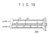
- Fig. 19 shows in a cross-sectional view an outline of structure of a third embodiment of a touch panel input device in accordance with the present invention.
- the structure of Fig. 19 includes a touch panel input device 200 as the third embodiment in accordance with the present invention.
- the third embodiment mainly includes two layers, i.e., layers A and B.
- the third embodiment differs from the first and second embodiments in that the second transparent film 14 shown in Fig. 7 is substituted for two independent transparent films 14a and 14b.
- layers A and B are electrically and/or structurally independent completely touch panels. By simply attaching two touch panels to each other, there can be implemented a device similar to the touch panels of the first and second embodiments.
- a general touch panel of the prior art is available.
- the material of the bottom section is changed from glass to a film. Consequently, a touch panel production process of the prior art can be directly used and hence the initial cost can be minimized and productivity can be increased.
- the touch panel input device of the present invention including two touch panels attached onto each other, when a position is inputted by a finger(tip) or a pen, information of the position indicated by the fingertip or a pen can be appropriately detected in any situation.
- the touch panel input device of the present invention when a position is inputted, it is possible to identify automatically that the input operation is conducted by a finger or a pen according to pressure received. Therefore, even if an erroneous input is caused, for example, by touching the touch panel by a hand in a pen input mode, the device can conduct control operation so that the erroneous input is appropriately rejected.
- the touch panel production process of the prior art can be employed as a production process. This lowers the initial cost and improves productivity.
Landscapes
- Engineering & Computer Science (AREA)
- General Engineering & Computer Science (AREA)
- Theoretical Computer Science (AREA)
- Human Computer Interaction (AREA)
- Physics & Mathematics (AREA)
- General Physics & Mathematics (AREA)
- Position Input By Displaying (AREA)
- Push-Button Switches (AREA)
Applications Claiming Priority (2)
| Application Number | Priority Date | Filing Date | Title |
|---|---|---|---|
| JP2000038189A JP2001222378A (ja) | 2000-02-10 | 2000-02-10 | タッチパネル入力装置 |
| JP2000038189 | 2000-02-10 |
Publications (2)
| Publication Number | Publication Date |
|---|---|
| EP1126406A2 true EP1126406A2 (fr) | 2001-08-22 |
| EP1126406A3 EP1126406A3 (fr) | 2008-04-02 |
Family
ID=18561961
Family Applications (1)
| Application Number | Title | Priority Date | Filing Date |
|---|---|---|---|
| EP01103126A Withdrawn EP1126406A3 (fr) | 2000-02-10 | 2001-02-09 | Dispositif d'entrée à écran tactile |
Country Status (6)
| Country | Link |
|---|---|
| US (1) | US6628269B2 (fr) |
| EP (1) | EP1126406A3 (fr) |
| JP (1) | JP2001222378A (fr) |
| CN (1) | CN100367426C (fr) |
| AU (1) | AU784145B2 (fr) |
| HK (1) | HK1039828A1 (fr) |
Cited By (1)
| Publication number | Priority date | Publication date | Assignee | Title |
|---|---|---|---|---|
| TWI666575B (zh) * | 2017-05-30 | 2019-07-21 | 禾瑞亞科技股份有限公司 | 觸控處理裝置、方法與系統 |
Families Citing this family (101)
| Publication number | Priority date | Publication date | Assignee | Title |
|---|---|---|---|---|
| JP2002328779A (ja) * | 2001-05-07 | 2002-11-15 | Matsushita Electric Ind Co Ltd | タッチパネルおよびこれを用いた電子機器 |
| JP2003005912A (ja) * | 2001-06-20 | 2003-01-10 | Hitachi Ltd | タッチパネル付きディスプレイ装置及び表示方法 |
| KR100769783B1 (ko) * | 2002-03-29 | 2007-10-24 | 가부시끼가이샤 도시바 | 표시 입력 장치 및 표시 입력 시스템 |
| GB0313808D0 (en) * | 2003-06-14 | 2003-07-23 | Binstead Ronald P | Improvements in touch technology |
| US7289111B2 (en) * | 2004-03-25 | 2007-10-30 | International Business Machines Corporation | Resistive touch pad with multiple regions of sensitivity |
| FI20045149L (fi) * | 2004-04-23 | 2005-10-24 | Nokia Corp | Käyttöliittymä |
| US20060066589A1 (en) * | 2004-09-29 | 2006-03-30 | Masanori Ozawa | Input device |
| US7417627B2 (en) * | 2004-10-27 | 2008-08-26 | Eastman Kodak Company | Sensing display |
| US7324095B2 (en) * | 2004-11-01 | 2008-01-29 | Hewlett-Packard Development Company, L.P. | Pressure-sensitive input device for data processing systems |
| US7230198B2 (en) * | 2004-11-12 | 2007-06-12 | Eastman Kodak Company | Flexible sheet for resistive touch screen |
| US7847789B2 (en) * | 2004-11-23 | 2010-12-07 | Microsoft Corporation | Reducing accidental touch-sensitive device activation |
| US20070115265A1 (en) * | 2005-11-21 | 2007-05-24 | Nokia Corporation | Mobile device and method |
| KR20080006666A (ko) * | 2006-07-13 | 2008-01-17 | 삼성전자주식회사 | 소프트 키보드를 이용한 데이터 처리 장치 및 그의 데이터처리 방법 |
| JP4768027B2 (ja) * | 2006-08-31 | 2011-09-07 | パイオニア株式会社 | マトリクス型タッチパネル装置 |
| KR101347291B1 (ko) | 2006-11-17 | 2014-01-03 | 삼성디스플레이 주식회사 | 터치 센서 내장형 평판표시패널과 이의 구동방법 및 이를포함한 평판표시장치 |
| JP4809783B2 (ja) * | 2007-01-26 | 2011-11-09 | 株式会社 日立ディスプレイズ | タッチパネル付き表示モジュール |
| US7742290B1 (en) | 2007-03-28 | 2010-06-22 | Motion Computing, Inc. | Portable computer with flip keyboard |
| EP1975766A3 (fr) * | 2007-03-30 | 2009-10-07 | Fujitsu Component Limited | Écran tactile |
| TWI340337B (en) * | 2007-05-15 | 2011-04-11 | Htc Corp | Electronic device |
| TWI460647B (zh) * | 2007-05-15 | 2014-11-11 | Htc Corp | 電子裝置與其軟體之使用者介面多重選擇方法 |
| US20080284750A1 (en) * | 2007-05-15 | 2008-11-20 | High Tech Computer, Corp. | Method for multiple selections for an electronic device and the software thereof |
| US8120586B2 (en) * | 2007-05-15 | 2012-02-21 | Htc Corporation | Electronic devices with touch-sensitive navigational mechanisms, and associated methods |
| TWI380201B (en) * | 2007-05-15 | 2012-12-21 | Htc Corp | Method for browsing a user interface for an electronic device and the software thereof |
| TWI337318B (en) * | 2007-05-15 | 2011-02-11 | Htc Corp | Electronic device operated by using touch display |
| TW200844813A (en) * | 2007-05-15 | 2008-11-16 | Htc Corp | Delay judgment systems and methods, and machine readable medium and related electronic devices thereof |
| TW200915820A (en) * | 2007-09-19 | 2009-04-01 | Giga Byte Tech Co Ltd | Touch panel structure having dual touch-modes, and signal processing method and device |
| TW200917111A (en) * | 2007-10-02 | 2009-04-16 | Himark Technology Inc | Resistive type multi-touch control panel and its detection method |
| CN101458599B (zh) * | 2007-12-14 | 2011-06-08 | 清华大学 | 触摸屏、触摸屏的制备方法及使用该触摸屏的显示装置 |
| CN101470558B (zh) * | 2007-12-27 | 2012-11-21 | 清华大学 | 触摸屏及显示装置 |
| CN101458602B (zh) * | 2007-12-12 | 2011-12-21 | 清华大学 | 触摸屏及显示装置 |
| CN101419518B (zh) * | 2007-10-23 | 2012-06-20 | 清华大学 | 触摸屏 |
| CN101464763B (zh) * | 2007-12-21 | 2010-09-29 | 清华大学 | 触摸屏的制备方法 |
| CN101458594B (zh) * | 2007-12-12 | 2012-07-18 | 清华大学 | 触摸屏及显示装置 |
| CN101458598B (zh) * | 2007-12-14 | 2011-06-08 | 清华大学 | 触摸屏及显示装置 |
| CN101656769B (zh) * | 2008-08-22 | 2012-10-10 | 清华大学 | 移动电话 |
| CN101458600B (zh) * | 2007-12-14 | 2011-11-30 | 清华大学 | 触摸屏及显示装置 |
| CN101470559B (zh) * | 2007-12-27 | 2012-11-21 | 清华大学 | 触摸屏及显示装置 |
| CN101458597B (zh) * | 2007-12-14 | 2011-06-08 | 清华大学 | 触摸屏、触摸屏的制备方法及使用该触摸屏的显示装置 |
| CN101458603B (zh) * | 2007-12-12 | 2011-06-08 | 北京富纳特创新科技有限公司 | 触摸屏及显示装置 |
| CN101419519B (zh) * | 2007-10-23 | 2012-06-20 | 清华大学 | 触摸屏 |
| CN101655720B (zh) * | 2008-08-22 | 2012-07-18 | 清华大学 | 个人数字助理 |
| CN101458605B (zh) * | 2007-12-12 | 2011-03-30 | 鸿富锦精密工业(深圳)有限公司 | 触摸屏及显示装置 |
| CN101458593B (zh) * | 2007-12-12 | 2012-03-14 | 清华大学 | 触摸屏及显示装置 |
| CN101676832B (zh) * | 2008-09-19 | 2012-03-28 | 清华大学 | 台式电脑 |
| CN101458608B (zh) * | 2007-12-14 | 2011-09-28 | 清华大学 | 触摸屏的制备方法 |
| CN101458604B (zh) * | 2007-12-12 | 2012-03-28 | 清华大学 | 触摸屏及显示装置 |
| CN101458609B (zh) * | 2007-12-14 | 2011-11-09 | 清华大学 | 触摸屏及显示装置 |
| CN101470566B (zh) * | 2007-12-27 | 2011-06-08 | 清华大学 | 触摸式控制装置 |
| CN101470560B (zh) * | 2007-12-27 | 2012-01-25 | 清华大学 | 触摸屏及显示装置 |
| CN101620454A (zh) * | 2008-07-04 | 2010-01-06 | 清华大学 | 便携式电脑 |
| CN101458595B (zh) * | 2007-12-12 | 2011-06-08 | 清华大学 | 触摸屏及显示装置 |
| CN101458596B (zh) * | 2007-12-12 | 2011-06-08 | 北京富纳特创新科技有限公司 | 触摸屏及显示装置 |
| CN101458606B (zh) * | 2007-12-12 | 2012-06-20 | 清华大学 | 触摸屏、触摸屏的制备方法及使用该触摸屏的显示装置 |
| TWI397006B (zh) * | 2007-10-30 | 2013-05-21 | Asustek Comp Inc | 觸控顯示裝置及判斷觸控方式之方法 |
| TWI340339B (en) * | 2007-11-08 | 2011-04-11 | Asustek Comp Inc | Touch device and a method of determining touch mode thereof |
| CN101458975B (zh) * | 2007-12-12 | 2012-05-16 | 清华大学 | 电子元件 |
| CN101464757A (zh) * | 2007-12-21 | 2009-06-24 | 清华大学 | 触摸屏及显示装置 |
| CN101458601B (zh) * | 2007-12-14 | 2012-03-14 | 清华大学 | 触摸屏及显示装置 |
| CN101458607B (zh) * | 2007-12-14 | 2010-12-29 | 清华大学 | 触摸屏及显示装置 |
| CN101470565B (zh) * | 2007-12-27 | 2011-08-24 | 清华大学 | 触摸屏及显示装置 |
| CN101464764B (zh) * | 2007-12-21 | 2012-07-18 | 清华大学 | 触摸屏及显示装置 |
| CN101464765B (zh) * | 2007-12-21 | 2011-01-05 | 鸿富锦精密工业(深圳)有限公司 | 触摸屏及显示装置 |
| CN101464766B (zh) * | 2007-12-21 | 2011-11-30 | 清华大学 | 触摸屏及显示装置 |
| US8574393B2 (en) * | 2007-12-21 | 2013-11-05 | Tsinghua University | Method for making touch panel |
| JP2008146679A (ja) * | 2008-02-18 | 2008-06-26 | Alps Electric Co Ltd | 入力装置及びそれを備えた電子機器 |
| US20090231288A1 (en) * | 2008-03-17 | 2009-09-17 | Inventec Corporation | Hand-held electronic device and combined input method thereof |
| US20090237374A1 (en) * | 2008-03-20 | 2009-09-24 | Motorola, Inc. | Transparent pressure sensor and method for using |
| US9018030B2 (en) * | 2008-03-20 | 2015-04-28 | Symbol Technologies, Inc. | Transparent force sensor and method of fabrication |
| US20090251422A1 (en) * | 2008-04-08 | 2009-10-08 | Honeywell International Inc. | Method and system for enhancing interaction of a virtual keyboard provided through a small touch screen |
| US8237677B2 (en) * | 2008-07-04 | 2012-08-07 | Tsinghua University | Liquid crystal display screen |
| US8390580B2 (en) * | 2008-07-09 | 2013-03-05 | Tsinghua University | Touch panel, liquid crystal display screen using the same, and methods for making the touch panel and the liquid crystal display screen |
| TW201013501A (en) * | 2008-09-22 | 2010-04-01 | Swenc Technology Co Ltd | Touch panel and electronic device thereof |
| TWI409674B (zh) * | 2008-11-25 | 2013-09-21 | Bruce C S Chou | 具多輸入訊息之微型觸控裝置 |
| US20100201633A1 (en) * | 2009-02-09 | 2010-08-12 | Ocular Lcd Inc. | Touch screen with improved optical performace |
| CN101924816B (zh) * | 2009-06-12 | 2013-03-20 | 清华大学 | 柔性手机 |
| JP2011007653A (ja) * | 2009-06-26 | 2011-01-13 | Toyota Motor Corp | 接触検出装置及びロボット |
| CN101996031A (zh) * | 2009-08-25 | 2011-03-30 | 鸿富锦精密工业(深圳)有限公司 | 具有触摸输入功能的电子装置及其触摸输入方法 |
| US8988191B2 (en) * | 2009-08-27 | 2015-03-24 | Symbol Technologies, Inc. | Systems and methods for pressure-based authentication of an input on a touch screen |
| JP5707694B2 (ja) * | 2009-12-04 | 2015-04-30 | ソニー株式会社 | 表示装置及び表示装置の制御方法 |
| US8558722B2 (en) * | 2009-12-10 | 2013-10-15 | Industrial Technology Research Institute | Touch apparatus, transparent scan electrode structure, and manufacturing method thereof |
| JP5427070B2 (ja) * | 2010-03-05 | 2014-02-26 | 株式会社ワコム | 位置検出装置 |
| KR20110103287A (ko) * | 2010-04-20 | 2011-09-20 | 삼성전기주식회사 | 저항막식 터치스크린의 멀티터치 식별방법 |
| US8963874B2 (en) * | 2010-07-31 | 2015-02-24 | Symbol Technologies, Inc. | Touch screen rendering system and method of operation thereof |
| TWI564757B (zh) | 2010-08-31 | 2017-01-01 | 萬國商業機器公司 | 具有觸控螢幕的電腦裝置與其操作方法及電腦可讀媒體 |
| US8648810B2 (en) * | 2011-02-14 | 2014-02-11 | Ko Ja (Cayman) Co., Ltd. | Integrated input apparatus |
| US20120206374A1 (en) * | 2011-02-14 | 2012-08-16 | Htc Corporation | Systems and methods for screen data management |
| CN103034351A (zh) * | 2011-09-29 | 2013-04-10 | 富泰华工业(深圳)有限公司 | 触摸屏电子装置及其虚拟键盘的显示和控制方法 |
| JP5840522B2 (ja) | 2012-02-08 | 2016-01-06 | 株式会社ジャパンディスプレイ | タッチパネル、表示装置および電子機器 |
| KR102102663B1 (ko) * | 2012-10-05 | 2020-04-22 | 삼성전자주식회사 | 휴대단말기의 사용 방법 및 장치 |
| TW201421374A (zh) | 2012-11-28 | 2014-06-01 | Au Optronics Corp | 觸碰感測系統及其操作方法 |
| JP6026346B2 (ja) | 2013-03-06 | 2016-11-16 | 日東電工株式会社 | 位置センサ |
| JP2014197367A (ja) * | 2013-03-06 | 2014-10-16 | 日東電工株式会社 | 位置センサ |
| JP2014197364A (ja) * | 2013-03-07 | 2014-10-16 | 日東電工株式会社 | 情報表示システム |
| KR102157270B1 (ko) | 2013-04-26 | 2020-10-23 | 삼성전자주식회사 | 펜을 이용하는 사용자 단말 장치 및 그 제어 방법 |
| JP2014219897A (ja) * | 2013-05-10 | 2014-11-20 | 日東電工株式会社 | 情報表示装置 |
| US20150138701A1 (en) * | 2013-11-19 | 2015-05-21 | Vandana SIKKA | Portable device, system, and method |
| JP2015215666A (ja) * | 2014-05-08 | 2015-12-03 | 日東電工株式会社 | 位置センサ |
| JP2015215668A (ja) * | 2014-05-08 | 2015-12-03 | 日東電工株式会社 | 情報表示システム |
| JP2015215667A (ja) * | 2014-05-08 | 2015-12-03 | 日東電工株式会社 | 情報表示装置 |
| US10275078B1 (en) * | 2017-03-20 | 2019-04-30 | Rockwell Collins, Inc. | Split resistive touch sensor |
| WO2019218307A1 (fr) * | 2018-05-17 | 2019-11-21 | 深圳市柔宇科技有限公司 | Dispositif électronique souple et procédé de détermination de sa position de flexion |
Family Cites Families (11)
| Publication number | Priority date | Publication date | Assignee | Title |
|---|---|---|---|---|
| JPS61155944A (ja) | 1984-12-28 | 1986-07-15 | Nippon Steel Corp | 高温物体の端部検出装置 |
| AU8118587A (en) * | 1986-11-17 | 1988-05-19 | Exicom Australia Pty Limited | Improved membrane keyboard |
| US4864084A (en) * | 1988-02-18 | 1989-09-05 | C.A.M. Graphics, Co., Inc. | Membrane-type touch panel |
| US4983787A (en) * | 1988-09-01 | 1991-01-08 | Takahiro Kunikane | Coordinate input unit |
| US5402151A (en) * | 1989-10-02 | 1995-03-28 | U.S. Philips Corporation | Data processing system with a touch screen and a digitizing tablet, both integrated in an input device |
| JPH0635596A (ja) | 1992-07-15 | 1994-02-10 | Hitachi Ltd | 一体形成型センサプレート |
| US5412161A (en) * | 1993-06-21 | 1995-05-02 | At&T Global Information Solutions Company | Handwriting capture system with segmented digitizer |
| JPH07319609A (ja) | 1994-05-25 | 1995-12-08 | Toshiba Corp | 抵抗膜タブレット入力装置及び抵抗膜タブレット入力装置を適用してなる情報処理装置 |
| KR970049350A (ko) * | 1995-12-19 | 1997-07-29 | 윤종용 | 터치패널 |
| JP2000194506A (ja) * | 1998-12-25 | 2000-07-14 | Nec Corp | タッチパネル |
| JP2001043003A (ja) | 1999-07-29 | 2001-02-16 | Matsushita Electric Ind Co Ltd | タッチパネル入力装置 |
-
2000
- 2000-02-10 JP JP2000038189A patent/JP2001222378A/ja active Pending
-
2001
- 2001-02-08 US US09/778,727 patent/US6628269B2/en not_active Expired - Fee Related
- 2001-02-09 EP EP01103126A patent/EP1126406A3/fr not_active Withdrawn
- 2001-02-09 AU AU18391/01A patent/AU784145B2/en not_active Ceased
- 2001-02-10 CN CNB011119594A patent/CN100367426C/zh not_active Expired - Fee Related
-
2002
- 2002-02-06 HK HK02100922.1A patent/HK1039828A1/zh unknown
Cited By (1)
| Publication number | Priority date | Publication date | Assignee | Title |
|---|---|---|---|---|
| TWI666575B (zh) * | 2017-05-30 | 2019-07-21 | 禾瑞亞科技股份有限公司 | 觸控處理裝置、方法與系統 |
Also Published As
| Publication number | Publication date |
|---|---|
| CN1308352A (zh) | 2001-08-15 |
| EP1126406A3 (fr) | 2008-04-02 |
| US6628269B2 (en) | 2003-09-30 |
| AU1839101A (en) | 2001-08-16 |
| US20010013861A1 (en) | 2001-08-16 |
| HK1039828A1 (zh) | 2002-05-10 |
| JP2001222378A (ja) | 2001-08-17 |
| AU784145B2 (en) | 2006-02-09 |
| CN100367426C (zh) | 2008-02-06 |
Similar Documents
| Publication | Publication Date | Title |
|---|---|---|
| US6628269B2 (en) | Touch panel input device capable of sensing input operation using a pen and a fingertip and method therefore | |
| US10671280B2 (en) | User input apparatus, computer connected to user input apparatus, and control method for computer connected to user input apparatus, and storage medium | |
| US8125454B2 (en) | Resistive type touch panel | |
| KR950012489B1 (ko) | 데이타 처리 시스템 및 그 처리 시간 감소 방법 | |
| JP5536809B2 (ja) | 感圧タッチ式制御装置 | |
| JP5536808B2 (ja) | 一体型タッチ式制御装置 | |
| US9575568B2 (en) | Multi-function keys providing additional functions and previews of functions | |
| KR101101581B1 (ko) | 멀티 포인트 터치 감지 장치 | |
| US20090009482A1 (en) | Touch sensor pad user input device | |
| US9335844B2 (en) | Combined touchpad and keypad using force input | |
| JPH0460715A (ja) | ペン入力装置 | |
| KR101149980B1 (ko) | 전자 장치의 디스플레이 스크린용 터치 센서 | |
| TWI396123B (zh) | 光學式觸控系統及其運作方法 | |
| US8154673B2 (en) | Touch panel and driving method thereof | |
| US8970498B2 (en) | Touch-enabled input device | |
| US20090135156A1 (en) | Touch sensor for a display screen of an electronic device | |
| US12204711B2 (en) | Attachment, input device, input method, and computer program | |
| JPH09330167A (ja) | ポインティング入力装置 | |
| EP4383053B1 (fr) | Dispositif d'affichage d'entrée | |
| US12056299B2 (en) | Input display device | |
| US20230176681A1 (en) | Hovering touch panel and hovering touch device | |
| KR100453174B1 (ko) | 터치패널의 구동장치 및 방법 | |
| JP6698912B2 (ja) | 入力表示装置及びプログラム | |
| HK1132343A (en) | Touch sensor for a display screen of an electronic device |
Legal Events
| Date | Code | Title | Description |
|---|---|---|---|
| PUAI | Public reference made under article 153(3) epc to a published international application that has entered the european phase |
Free format text: ORIGINAL CODE: 0009012 |
|
| AK | Designated contracting states |
Kind code of ref document: A2 Designated state(s): AT BE CH CY DE DK ES FI FR GB GR IE IT LI LU MC NL PT SE TR |
|
| AX | Request for extension of the european patent |
Free format text: AL;LT;LV;MK;RO;SI |
|
| PUAL | Search report despatched |
Free format text: ORIGINAL CODE: 0009013 |
|
| RIC1 | Information provided on ipc code assigned before grant |
Ipc: G06F 3/033 20060101AFI20080214BHEP |
|
| AK | Designated contracting states |
Kind code of ref document: A3 Designated state(s): AT BE CH CY DE DK ES FI FR GB GR IE IT LI LU MC NL PT SE TR |
|
| AX | Request for extension of the european patent |
Extension state: AL LT LV MK RO SI |
|
| 17P | Request for examination filed |
Effective date: 20080703 |
|
| 17Q | First examination report despatched |
Effective date: 20080819 |
|
| AKX | Designation fees paid |
Designated state(s): DE FR GB IT |
|
| STAA | Information on the status of an ep patent application or granted ep patent |
Free format text: STATUS: THE APPLICATION HAS BEEN WITHDRAWN |
|
| 18W | Application withdrawn |
Effective date: 20081229 |