EP1126477A2 - Procédé d'examen de structures dans un substrat sémiconducteur - Google Patents
Procédé d'examen de structures dans un substrat sémiconducteur Download PDFInfo
- Publication number
- EP1126477A2 EP1126477A2 EP20010103184 EP01103184A EP1126477A2 EP 1126477 A2 EP1126477 A2 EP 1126477A2 EP 20010103184 EP20010103184 EP 20010103184 EP 01103184 A EP01103184 A EP 01103184A EP 1126477 A2 EP1126477 A2 EP 1126477A2
- Authority
- EP
- European Patent Office
- Prior art keywords
- ray
- structures
- microscope
- radiation
- wavelength
- Prior art date
- Legal status (The legal status is an assumption and is not a legal conclusion. Google has not performed a legal analysis and makes no representation as to the accuracy of the status listed.)
- Withdrawn
Links
- GDOPTJXRTPNYNR-UHFFFAOYSA-N CC1CCCC1 Chemical compound CC1CCCC1 GDOPTJXRTPNYNR-UHFFFAOYSA-N 0.000 description 1
Images


Classifications
-
- G—PHYSICS
- G21—NUCLEAR PHYSICS; NUCLEAR ENGINEERING
- G21K—HANDLING OF PARTICLES OR IONISING RADIATION NOT OTHERWISE PROVIDED FOR; IRRADIATION DEVICES; GAMMA RAY OR X-RAY MICROSCOPES
- G21K7/00—Gamma- or X-ray microscopes
-
- G—PHYSICS
- G01—MEASURING; TESTING
- G01N—INVESTIGATING OR ANALYSING MATERIALS BY DETERMINING THEIR CHEMICAL OR PHYSICAL PROPERTIES
- G01N23/00—Investigating or analysing materials by the use of wave or particle radiation, e.g. X-rays or neutrons, not covered by groups G01N3/00 – G01N17/00, G01N21/00 or G01N22/00
- G01N23/02—Investigating or analysing materials by the use of wave or particle radiation, e.g. X-rays or neutrons, not covered by groups G01N3/00 – G01N17/00, G01N21/00 or G01N22/00 by transmitting the radiation through the material
- G01N23/04—Investigating or analysing materials by the use of wave or particle radiation, e.g. X-rays or neutrons, not covered by groups G01N3/00 – G01N17/00, G01N21/00 or G01N22/00 by transmitting the radiation through the material and forming images of the material
- G01N23/041—Phase-contrast imaging, e.g. using grating interferometers
-
- G—PHYSICS
- G21—NUCLEAR PHYSICS; NUCLEAR ENGINEERING
- G21K—HANDLING OF PARTICLES OR IONISING RADIATION NOT OTHERWISE PROVIDED FOR; IRRADIATION DEVICES; GAMMA RAY OR X-RAY MICROSCOPES
- G21K2207/00—Particular details of imaging devices or methods using ionizing electromagnetic radiation such as X-rays or gamma rays
- G21K2207/005—Methods and devices obtaining contrast from non-absorbing interaction of the radiation with matter, e.g. phase contrast
Definitions
- the thickness of the silicon wafer being preferred should be between 10 ⁇ m and 30 ⁇ m.
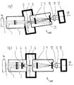
- the object 7 is illuminated using an X-ray condenser 3.
- a radiation-impermeable diaphragm 4 arranged in the middle of the resulting radiation cone brings about a hollow-cone-shaped illumination of the object 7.
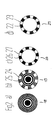
- a segmented phase ring 20 can be arranged in the rear focal plane of the x-ray objective 8. This arrangement is shown in Figure 3a.
- the segmented phase ring 20 consists of many phase-shifting and non-phase-shifting sections 26, 27.
- the segmented diaphragm 29 can be omitted, by using an annular condenser zone plate 19 as the X-ray condenser 3 (Fig.2b) is used in which only the phase ring corresponding Segments 25 with zone sections and zone-free segments 24 are structured. If the condenser zone plate 19 or the segmented phase ring 20 (Fig.2c) rotated appropriately, so can of the Imaging in phase contrast for imaging in the amplitude contrast image are switched: In phase contrast, the condenser 3 is such that the 0th order light of the object 7 only through the phase shifting Segments 26 of the phase ring 20 falls, while in the amplitude contrast Radiation of the 0th order only falls into the segments 27 in between. In all other intermediate positions of segmented phase ring 20 and one Condenser zone plate 19 with zone-free segments 24 and Zone sections 25 to one another can have any intermediate values Phase shift can be set.
- the spatially resolving detector device consists of imaging x-ray microscopes 100 from the x-ray converter 9, the Lens 11 and the camera 12.
- the camera 12 records the image. Because of the possible damage to the camera 12 with direct irradiation with very short wavelengths are best from the real X-ray image initially generates visible radiation, e.g. by means of a fluorescent Material of the X-ray converter 9, e.g. a phosphor.
- the visible one Radiation 10 is then applied to camera 12 for visible light, e.g. one CCD detector imaged by means of the optics 11, which e.g. one can include deflecting mirror - to the camera 12 from the direct X-ray and thus any possible radiation damage from Remove x-rays.
Landscapes
- Physics & Mathematics (AREA)
- Health & Medical Sciences (AREA)
- General Health & Medical Sciences (AREA)
- General Physics & Mathematics (AREA)
- Life Sciences & Earth Sciences (AREA)
- Chemical & Material Sciences (AREA)
- Analytical Chemistry (AREA)
- Biochemistry (AREA)
- Nuclear Medicine, Radiotherapy & Molecular Imaging (AREA)
- Radiology & Medical Imaging (AREA)
- Immunology (AREA)
- Pathology (AREA)
- Engineering & Computer Science (AREA)
- General Engineering & Computer Science (AREA)
- High Energy & Nuclear Physics (AREA)
- Analysing Materials By The Use Of Radiation (AREA)
- Testing Or Measuring Of Semiconductors Or The Like (AREA)
Applications Claiming Priority (2)
| Application Number | Priority Date | Filing Date | Title |
|---|---|---|---|
| US18237500P | 2000-02-14 | 2000-02-14 | |
| US182375P | 2000-02-14 |
Publications (2)
| Publication Number | Publication Date |
|---|---|
| EP1126477A2 true EP1126477A2 (fr) | 2001-08-22 |
| EP1126477A3 EP1126477A3 (fr) | 2003-06-18 |
Family
ID=22668185
Family Applications (1)
| Application Number | Title | Priority Date | Filing Date |
|---|---|---|---|
| EP01103184A Withdrawn EP1126477A3 (fr) | 2000-02-14 | 2001-02-10 | Procédé d'examen de structures dans un substrat sémiconducteur |
Country Status (3)
| Country | Link |
|---|---|
| US (1) | US6859516B2 (fr) |
| EP (1) | EP1126477A3 (fr) |
| JP (1) | JP2001305077A (fr) |
Cited By (4)
| Publication number | Priority date | Publication date | Assignee | Title |
|---|---|---|---|---|
| EP1503386A3 (fr) * | 2003-07-26 | 2009-08-05 | Bruker AXS GmbH | Miroir encapsulé pour rayons-X |
| WO2014039644A1 (fr) * | 2012-09-05 | 2014-03-13 | Svxr Llc | Microscope d'inspection à rayons x haute vitesse |
| US10153062B2 (en) | 2015-06-30 | 2018-12-11 | Fraunhofer-Gesellschaft Zur Foerderung Der Angewandten Forschung E.V. | Illumination and imaging device for high-resolution X-ray microscopy with high photon energy |
| WO2024078883A1 (fr) | 2022-10-14 | 2024-04-18 | Carl Zeiss Smt Gmbh | Procédé d'obtention d'informations pour commander un processus de fabrication d'un dispositif semi-conducteur empilé et système de détection faisant appel à ce procédé |
Families Citing this family (46)
| Publication number | Priority date | Publication date | Assignee | Title |
|---|---|---|---|---|
| JP4110390B2 (ja) * | 2002-03-19 | 2008-07-02 | セイコーエプソン株式会社 | 半導体装置の製造方法 |
| DE50313254D1 (de) * | 2002-05-10 | 2010-12-23 | Zeiss Carl Smt Ag | Reflektives roentgenmikroskop zur untersuchung von objekten mit wellenlaengen = 100nm in reflexion |
| US20050282300A1 (en) * | 2002-05-29 | 2005-12-22 | Xradia, Inc. | Back-end-of-line metallization inspection and metrology microscopy system and method using x-ray fluorescence |
| US7312432B2 (en) * | 2002-07-08 | 2007-12-25 | Dmetrix, Inc. | Single axis illumination for multi-axis imaging system |
| DE10234589A1 (de) * | 2002-07-30 | 2004-02-12 | Robert Bosch Gmbh | Schichtsystem mit einer Siliziumschicht und einer Passivierschicht, Verfahren zur Erzeugung einer Passivierschicht auf einer Siliziumschicht und deren Verwendung |
| US7394890B1 (en) * | 2003-11-07 | 2008-07-01 | Xradia, Inc. | Optimized x-ray energy for high resolution imaging of integrated circuits structures |
| US7170969B1 (en) * | 2003-11-07 | 2007-01-30 | Xradia, Inc. | X-ray microscope capillary condenser system |
| US7551722B2 (en) * | 2004-04-08 | 2009-06-23 | Japan Science And Technology Agency | X-ray target and apparatuses using the same |
| US7231617B2 (en) * | 2004-09-17 | 2007-06-12 | International Business Machines Corporation | Determination of grain sizes of electrically conductive lines in semiconductor integrated circuits |
| US7406151B1 (en) * | 2005-07-19 | 2008-07-29 | Xradia, Inc. | X-ray microscope with microfocus source and Wolter condenser |
| KR100651055B1 (ko) * | 2005-08-30 | 2006-12-01 | 학교법인 원광학원 | 연 엑스선 현미경 장치 |
| US7443953B1 (en) * | 2005-12-09 | 2008-10-28 | Xradia, Inc. | Structured anode X-ray source for X-ray microscopy |
| DE502006007410D1 (de) * | 2005-12-27 | 2010-08-26 | Paul Scherrer Inst Psi | Fokus-Detektor-Anordnung zur Erzeugung von Phasenkontrast-Röntgenaufnahmen und Verfahren hierzu |
| DE102006037257B4 (de) * | 2006-02-01 | 2017-06-01 | Siemens Healthcare Gmbh | Verfahren und Messanordnung zur zerstörungsfreien Analyse eines Untersuchungsobjektes mit Röntgenstrahlung |
| JP4700034B2 (ja) * | 2007-08-13 | 2011-06-15 | 日本電信電話株式会社 | X線集光レンズ |
| JP4659015B2 (ja) * | 2007-11-14 | 2011-03-30 | 日本電信電話株式会社 | X線集光レンズ |
| US8174695B2 (en) * | 2008-08-15 | 2012-05-08 | The United States Of America As Represented By The Administrator Of The National Aeronautics And Space Administration | Arrayed micro-ring spectrometer system and method of use |
| US8018815B2 (en) * | 2008-08-15 | 2011-09-13 | The United States Of America As Represented By The Administrator Of The National Aeronautics And Space Administration | Micro-Fresnel zone plate optical devices using densely accumulated ray points |
| DE102009009602A1 (de) * | 2008-10-27 | 2010-04-29 | Ifg - Institute For Scientific Instruments Gmbh | Spektralauflösende elektronische Röntgenkamera |
| CN102365052B (zh) * | 2009-03-27 | 2015-05-13 | 皇家飞利浦电子股份有限公司 | 利用圆形光栅进行差分相衬成像 |
| US8294989B2 (en) * | 2009-07-30 | 2012-10-23 | The United States Of America As Represented By The Administrator Of The National Aeronautics And Space Administration | Apparatus and method for creating a photonic densely-accumulated ray-point |
| JP2011086693A (ja) * | 2009-10-14 | 2011-04-28 | Nippon Inter Electronics Corp | 半導体装置の検査システムおよび方法 |
| US8450688B2 (en) | 2009-11-05 | 2013-05-28 | The Aerospace Corporation | Refraction assisted illumination for imaging |
| US8461532B2 (en) * | 2009-11-05 | 2013-06-11 | The Aerospace Corporation | Refraction assisted illumination for imaging |
| US8138476B2 (en) * | 2009-11-05 | 2012-03-20 | The Aerospace Corporation | Refraction assisted illumination for imaging |
| US8790533B2 (en) * | 2010-04-23 | 2014-07-29 | Postech Academy-Industry Foundation | Method of etching semiconductor nanocrystals |
| FR2978566B1 (fr) * | 2011-07-25 | 2016-10-28 | Commissariat Energie Atomique | Systeme d'imagerie pour l'imagerie d'objets a mouvement rapide |
| US9007454B2 (en) | 2012-10-31 | 2015-04-14 | The Aerospace Corporation | Optimized illumination for imaging |
| US20150055745A1 (en) * | 2013-08-23 | 2015-02-26 | Carl Zeiss X-ray Microscopy, Inc. | Phase Contrast Imaging Using Patterned Illumination/Detector and Phase Mask |
| JP7069670B2 (ja) * | 2017-12-04 | 2022-05-18 | コニカミノルタ株式会社 | X線撮影システム |
| WO2020219254A1 (fr) | 2019-04-24 | 2020-10-29 | Laitram, L.L.C. | Bande transporteuse et module avec plaques d'usure |
| US11175243B1 (en) * | 2020-02-06 | 2021-11-16 | Sigray, Inc. | X-ray dark-field in-line inspection for semiconductor samples |
| CN115667896B (zh) | 2020-05-18 | 2024-06-21 | 斯格瑞公司 | 使用晶体分析器和多个检测元件的x射线吸收光谱的系统和方法 |
| JP7640682B2 (ja) | 2020-09-17 | 2025-03-05 | シグレイ、インコーポレイテッド | X線を用いた深さ分解計測および分析のためのシステムおよび方法 |
| US12480892B2 (en) | 2020-12-07 | 2025-11-25 | Sigray, Inc. | High throughput 3D x-ray imaging system using a transmission x-ray source |
| KR102927910B1 (ko) | 2020-12-07 | 2026-02-19 | 시그레이, 아이엔씨. | 투과 x-선 소스를 이용한 고처리량 3D x-선 이미징 시스템 |
| US12360067B2 (en) | 2022-03-02 | 2025-07-15 | Sigray, Inc. | X-ray fluorescence system and x-ray source with electrically insulative target material |
| DE112023001408T5 (de) | 2022-03-15 | 2025-02-13 | Sigray, Inc. | System und verfahren für die kompakte laminographie unter verwendung einer mikrofokus-transmissionsröntgenquelle und eines röntgendetektors mit variabler vergrösserung |
| WO2023203994A1 (fr) * | 2022-04-19 | 2023-10-26 | コニカミノルタ株式会社 | Procédé de traçage de changement d'état et système de traçage de changement d'état |
| DE112023002079T5 (de) | 2022-05-02 | 2025-02-27 | Sigray, Inc. | Sequenzielles wellenlängendispersives röntgenspektrometer |
| WO2024173256A1 (fr) | 2023-02-16 | 2024-08-22 | Sigray, Inc. | Système détecteur de rayons x avec au moins deux diffracteurs de bragg plats empilés |
| US12181423B1 (en) | 2023-09-07 | 2024-12-31 | Sigray, Inc. | Secondary image removal using high resolution x-ray transmission sources |
| WO2025101530A1 (fr) | 2023-11-07 | 2025-05-15 | Sigray, Inc. | Système et procédé de spectroscopie d'absorption des rayons x utilisant des informations spectrales provenant de deux plans orthogonaux |
| WO2025151383A1 (fr) | 2024-01-08 | 2025-07-17 | Sigray, Inc. | Système d'analyse par rayons x à faisceau de rayons x focalisé et à microscope non à rayons x |
| WO2025155719A1 (fr) | 2024-01-18 | 2025-07-24 | Sigray, Inc. | Réseau séquentiel de détecteurs d'imagerie par rayons x |
| WO2025174966A1 (fr) | 2024-02-15 | 2025-08-21 | Sigray, Inc. | Système et procédé de génération d'un faisceau de rayons x focalisé |
Family Cites Families (10)
| Publication number | Priority date | Publication date | Assignee | Title |
|---|---|---|---|---|
| ZA79531B (en) * | 1978-02-14 | 1980-02-27 | De Beers Cons Mines Ltd | Improvements in radiography |
| JPH02203261A (ja) * | 1989-02-01 | 1990-08-13 | Fujitsu Ltd | 物体内部検査方法 |
| DE4027285A1 (de) * | 1990-08-29 | 1992-03-05 | Zeiss Carl Fa | Roentgenmikroskop |
| US5177774A (en) * | 1991-08-23 | 1993-01-05 | Trustees Of Princeton University | Reflection soft X-ray microscope and method |
| US5432831A (en) * | 1992-09-10 | 1995-07-11 | Olympus Optical Co., Ltd. | Vacuum optical system |
| US5434901A (en) * | 1992-12-07 | 1995-07-18 | Olympus Optical Co., Ltd. | Soft X-ray microscope |
| US5450463A (en) * | 1992-12-25 | 1995-09-12 | Olympus Optical Co., Ltd. | X-ray microscope |
| DE4432811B4 (de) * | 1993-09-15 | 2006-04-13 | Carl Zeiss | Phasenkontrast-Röntgenmikroskop |
| US5703361A (en) * | 1996-04-30 | 1997-12-30 | The United States Of America As Represented By The Secretary Of The Army | Circuit scanning device and method |
| DE69836730T2 (de) * | 1997-04-08 | 2007-10-04 | Xrt Ltd. | Hochauflösende röntgenbilderdarstellung von sehr kleinen objekten |
-
2001
- 2001-02-10 EP EP01103184A patent/EP1126477A3/fr not_active Withdrawn
- 2001-02-14 JP JP2001037201A patent/JP2001305077A/ja not_active Withdrawn
- 2001-02-14 US US09/681,186 patent/US6859516B2/en not_active Expired - Lifetime
Non-Patent Citations (1)
| Title |
|---|
| None * |
Cited By (7)
| Publication number | Priority date | Publication date | Assignee | Title |
|---|---|---|---|---|
| EP1503386A3 (fr) * | 2003-07-26 | 2009-08-05 | Bruker AXS GmbH | Miroir encapsulé pour rayons-X |
| WO2014039644A1 (fr) * | 2012-09-05 | 2014-03-13 | Svxr Llc | Microscope d'inspection à rayons x haute vitesse |
| US9129715B2 (en) | 2012-09-05 | 2015-09-08 | SVXR, Inc. | High speed x-ray inspection microscope |
| US9607724B2 (en) | 2012-09-05 | 2017-03-28 | SVXR, Inc. | Devices processed using x-rays |
| US9646732B2 (en) | 2012-09-05 | 2017-05-09 | SVXR, Inc. | High speed X-ray microscope |
| US10153062B2 (en) | 2015-06-30 | 2018-12-11 | Fraunhofer-Gesellschaft Zur Foerderung Der Angewandten Forschung E.V. | Illumination and imaging device for high-resolution X-ray microscopy with high photon energy |
| WO2024078883A1 (fr) | 2022-10-14 | 2024-04-18 | Carl Zeiss Smt Gmbh | Procédé d'obtention d'informations pour commander un processus de fabrication d'un dispositif semi-conducteur empilé et système de détection faisant appel à ce procédé |
Also Published As
| Publication number | Publication date |
|---|---|
| US6859516B2 (en) | 2005-02-22 |
| JP2001305077A (ja) | 2001-10-31 |
| EP1126477A3 (fr) | 2003-06-18 |
| US20010046276A1 (en) | 2001-11-29 |
Similar Documents
| Publication | Publication Date | Title |
|---|---|---|
| EP1126477A2 (fr) | Procédé d'examen de structures dans un substrat sémiconducteur | |
| US11619596B2 (en) | X-ray photoemission system for 3-D laminography | |
| Matsui et al. | Photoelectron momentum microscope at BL6U of UVSOR-III synchrotron | |
| DE69836730T2 (de) | Hochauflösende röntgenbilderdarstellung von sehr kleinen objekten | |
| US7183547B2 (en) | Element-specific X-ray fluorescence microscope and method of operation | |
| DE602004002031T2 (de) | Hochauflösende Defekterkennung mit Positronenrekombination durch gleichzeitiges Einstrahlen eines Positronenstrahls und eines Elektronenstrahls | |
| DE69325157T2 (de) | Methode und vorrichtung zur oberflächenanalyse | |
| DE60308482T2 (de) | Vorrichtung und Verfahren zur Untersuchung einer Probe eines Spezimen mittels eines Elektronenstrahls | |
| DE68924563T2 (de) | Verfahren und Vorrichtung zur Oberflächenanalyse. | |
| Yaguchi et al. | Observation of three-dimensional elemental distributions of a Si device using a 360°-tilt FIB and the cold field-emission STEM system | |
| Herbst et al. | Spot spectroscopy: Local spectroscopic measurements within laser‐produced plasmas | |
| JP2001512568A (ja) | 軟x線顕微透視装置 | |
| DE19620821A1 (de) | Elektronenmikroskop und Probenbetrachtungsverfahren unter Verwendung desselben | |
| US5864599A (en) | X-ray moire microscope | |
| JPWO1997001862A1 (ja) | 電子顕微鏡および電子顕微方法 | |
| WO1997001862A1 (fr) | Microscope electronique et microscopie electronique | |
| Gürsoy et al. | Multimodal x-ray nanotomography | |
| Lau et al. | Non destructive failure analysis technique with a laboratory based 3D X-ray nanotomography system | |
| Cerrina | X-ray photo-electron spectromicroscopy | |
| Matruglio et al. | A novel approach in the free-electron laser diagnosis based on a pixelated phosphor detector | |
| Stead et al. | Soft x-ray contact microscopy of biological specimens: Aluminum-coated silicon nitride windows as XUV filters | |
| Coleman et al. | The UEA positron re-emission microscope: first images | |
| Michette | X-ray Microscopy | |
| Kimoto et al. | Scanning electron microscope as a tool in geology and biology | |
| Wang et al. | X-ray microscopy for NDE of micro-and nano-structrues |
Legal Events
| Date | Code | Title | Description |
|---|---|---|---|
| PUAI | Public reference made under article 153(3) epc to a published international application that has entered the european phase |
Free format text: ORIGINAL CODE: 0009012 |
|
| AK | Designated contracting states |
Kind code of ref document: A2 Designated state(s): AT BE CH CY DE DK ES FI FR GB GR IE IT LI LU MC NL PT SE TR |
|
| AX | Request for extension of the european patent |
Free format text: AL;LT;LV;MK;RO;SI |
|
| RIC1 | Information provided on ipc code assigned before grant |
Ipc: 7G 01N 23/08 B Ipc: 7G 01N 23/04 B Ipc: 7G 21K 7/00 A |
|
| PUAL | Search report despatched |
Free format text: ORIGINAL CODE: 0009013 |
|
| AK | Designated contracting states |
Designated state(s): AT BE CH CY DE DK ES FI FR GB GR IE IT LI LU MC NL PT SE TR |
|
| AX | Request for extension of the european patent |
Extension state: AL LT LV MK RO SI |
|
| 17P | Request for examination filed |
Effective date: 20031025 |
|
| AKX | Designation fees paid |
Designated state(s): DE FR GB |
|
| 17Q | First examination report despatched |
Effective date: 20070110 |
|
| STAA | Information on the status of an ep patent application or granted ep patent |
Free format text: STATUS: THE APPLICATION IS DEEMED TO BE WITHDRAWN |
|
| 18D | Application deemed to be withdrawn |
Effective date: 20070522 |