EP1126519A2 - Struktur und Herstellungsmethode von Anschlussflächen auf verkupferten intergrierten Schaltungen - Google Patents
Struktur und Herstellungsmethode von Anschlussflächen auf verkupferten intergrierten Schaltungen Download PDFInfo
- Publication number
- EP1126519A2 EP1126519A2 EP01000021A EP01000021A EP1126519A2 EP 1126519 A2 EP1126519 A2 EP 1126519A2 EP 01000021 A EP01000021 A EP 01000021A EP 01000021 A EP01000021 A EP 01000021A EP 1126519 A2 EP1126519 A2 EP 1126519A2
- Authority
- EP
- European Patent Office
- Prior art keywords
- metal
- copper
- layer
- barrier metal
- bondable
- Prior art date
- Legal status (The legal status is an assumption and is not a legal conclusion. Google has not performed a legal analysis and makes no representation as to the accuracy of the status listed.)
- Withdrawn
Links
Images

Classifications
-
- H—ELECTRICITY
- H10—SEMICONDUCTOR DEVICES; ELECTRIC SOLID-STATE DEVICES NOT OTHERWISE PROVIDED FOR
- H10W—GENERIC PACKAGES, INTERCONNECTIONS, CONNECTORS OR OTHER CONSTRUCTIONAL DETAILS OF DEVICES COVERED BY CLASS H10
- H10W72/00—Interconnections or connectors in packages
- H10W72/071—Connecting or disconnecting
-
- H—ELECTRICITY
- H10—SEMICONDUCTOR DEVICES; ELECTRIC SOLID-STATE DEVICES NOT OTHERWISE PROVIDED FOR
- H10W—GENERIC PACKAGES, INTERCONNECTIONS, CONNECTORS OR OTHER CONSTRUCTIONAL DETAILS OF DEVICES COVERED BY CLASS H10
- H10W20/00—Interconnections in chips, wafers or substrates
- H10W20/40—Interconnections external to wafers or substrates, e.g. back-end-of-line [BEOL] metallisations or vias connecting to gate electrodes
- H10W20/41—Interconnections external to wafers or substrates, e.g. back-end-of-line [BEOL] metallisations or vias connecting to gate electrodes characterised by their conductive parts
- H10W20/44—Conductive materials thereof
- H10W20/4403—Conductive materials thereof based on metals, e.g. alloys, metal silicides
- H10W20/4421—Conductive materials thereof based on metals, e.g. alloys, metal silicides the principal metal being copper
- H10W20/4424—Copper alloys
-
- H—ELECTRICITY
- H10—SEMICONDUCTOR DEVICES; ELECTRIC SOLID-STATE DEVICES NOT OTHERWISE PROVIDED FOR
- H10W—GENERIC PACKAGES, INTERCONNECTIONS, CONNECTORS OR OTHER CONSTRUCTIONAL DETAILS OF DEVICES COVERED BY CLASS H10
- H10W20/00—Interconnections in chips, wafers or substrates
- H10W20/40—Interconnections external to wafers or substrates, e.g. back-end-of-line [BEOL] metallisations or vias connecting to gate electrodes
- H10W20/41—Interconnections external to wafers or substrates, e.g. back-end-of-line [BEOL] metallisations or vias connecting to gate electrodes characterised by their conductive parts
- H10W20/425—Barrier, adhesion or liner layers
-
- H—ELECTRICITY
- H10—SEMICONDUCTOR DEVICES; ELECTRIC SOLID-STATE DEVICES NOT OTHERWISE PROVIDED FOR
- H10W—GENERIC PACKAGES, INTERCONNECTIONS, CONNECTORS OR OTHER CONSTRUCTIONAL DETAILS OF DEVICES COVERED BY CLASS H10
- H10W72/00—Interconnections or connectors in packages
- H10W72/01—Manufacture or treatment
- H10W72/019—Manufacture or treatment of bond pads
-
- H—ELECTRICITY
- H10—SEMICONDUCTOR DEVICES; ELECTRIC SOLID-STATE DEVICES NOT OTHERWISE PROVIDED FOR
- H10W—GENERIC PACKAGES, INTERCONNECTIONS, CONNECTORS OR OTHER CONSTRUCTIONAL DETAILS OF DEVICES COVERED BY CLASS H10
- H10W20/00—Interconnections in chips, wafers or substrates
- H10W20/40—Interconnections external to wafers or substrates, e.g. back-end-of-line [BEOL] metallisations or vias connecting to gate electrodes
- H10W20/41—Interconnections external to wafers or substrates, e.g. back-end-of-line [BEOL] metallisations or vias connecting to gate electrodes characterised by their conductive parts
- H10W20/44—Conductive materials thereof
- H10W20/4403—Conductive materials thereof based on metals, e.g. alloys, metal silicides
- H10W20/4421—Conductive materials thereof based on metals, e.g. alloys, metal silicides the principal metal being copper
-
- H—ELECTRICITY
- H10—SEMICONDUCTOR DEVICES; ELECTRIC SOLID-STATE DEVICES NOT OTHERWISE PROVIDED FOR
- H10W—GENERIC PACKAGES, INTERCONNECTIONS, CONNECTORS OR OTHER CONSTRUCTIONAL DETAILS OF DEVICES COVERED BY CLASS H10
- H10W72/00—Interconnections or connectors in packages
- H10W72/01—Manufacture or treatment
- H10W72/015—Manufacture or treatment of bond wires
- H10W72/01551—Changing the shapes of bond wires
-
- H—ELECTRICITY
- H10—SEMICONDUCTOR DEVICES; ELECTRIC SOLID-STATE DEVICES NOT OTHERWISE PROVIDED FOR
- H10W—GENERIC PACKAGES, INTERCONNECTIONS, CONNECTORS OR OTHER CONSTRUCTIONAL DETAILS OF DEVICES COVERED BY CLASS H10
- H10W72/00—Interconnections or connectors in packages
- H10W72/071—Connecting or disconnecting
- H10W72/0711—Apparatus therefor
- H10W72/07141—Means for applying energy, e.g. ovens or lasers
-
- H—ELECTRICITY
- H10—SEMICONDUCTOR DEVICES; ELECTRIC SOLID-STATE DEVICES NOT OTHERWISE PROVIDED FOR
- H10W—GENERIC PACKAGES, INTERCONNECTIONS, CONNECTORS OR OTHER CONSTRUCTIONAL DETAILS OF DEVICES COVERED BY CLASS H10
- H10W72/00—Interconnections or connectors in packages
- H10W72/071—Connecting or disconnecting
- H10W72/075—Connecting or disconnecting of bond wires
- H10W72/07511—Treating the bonding area before connecting, e.g. by applying flux or cleaning
-
- H—ELECTRICITY
- H10—SEMICONDUCTOR DEVICES; ELECTRIC SOLID-STATE DEVICES NOT OTHERWISE PROVIDED FOR
- H10W—GENERIC PACKAGES, INTERCONNECTIONS, CONNECTORS OR OTHER CONSTRUCTIONAL DETAILS OF DEVICES COVERED BY CLASS H10
- H10W72/00—Interconnections or connectors in packages
- H10W72/071—Connecting or disconnecting
- H10W72/075—Connecting or disconnecting of bond wires
- H10W72/07531—Techniques
- H10W72/07532—Compression bonding, e.g. thermocompression bonding
- H10W72/07533—Ultrasonic bonding, e.g. thermosonic bonding
-
- H—ELECTRICITY
- H10—SEMICONDUCTOR DEVICES; ELECTRIC SOLID-STATE DEVICES NOT OTHERWISE PROVIDED FOR
- H10W—GENERIC PACKAGES, INTERCONNECTIONS, CONNECTORS OR OTHER CONSTRUCTIONAL DETAILS OF DEVICES COVERED BY CLASS H10
- H10W72/00—Interconnections or connectors in packages
- H10W72/50—Bond wires
- H10W72/531—Shapes of wire connectors
- H10W72/533—Cross-sectional shape
- H10W72/534—Cross-sectional shape being rectangular
-
- H—ELECTRICITY
- H10—SEMICONDUCTOR DEVICES; ELECTRIC SOLID-STATE DEVICES NOT OTHERWISE PROVIDED FOR
- H10W—GENERIC PACKAGES, INTERCONNECTIONS, CONNECTORS OR OTHER CONSTRUCTIONAL DETAILS OF DEVICES COVERED BY CLASS H10
- H10W72/00—Interconnections or connectors in packages
- H10W72/50—Bond wires
- H10W72/531—Shapes of wire connectors
- H10W72/536—Shapes of wire connectors the connected ends being ball-shaped
-
- H—ELECTRICITY
- H10—SEMICONDUCTOR DEVICES; ELECTRIC SOLID-STATE DEVICES NOT OTHERWISE PROVIDED FOR
- H10W—GENERIC PACKAGES, INTERCONNECTIONS, CONNECTORS OR OTHER CONSTRUCTIONAL DETAILS OF DEVICES COVERED BY CLASS H10
- H10W72/00—Interconnections or connectors in packages
- H10W72/50—Bond wires
- H10W72/551—Materials of bond wires
- H10W72/552—Materials of bond wires comprising metals or metalloids, e.g. silver
- H10W72/5522—Materials of bond wires comprising metals or metalloids, e.g. silver comprising gold [Au]
-
- H—ELECTRICITY
- H10—SEMICONDUCTOR DEVICES; ELECTRIC SOLID-STATE DEVICES NOT OTHERWISE PROVIDED FOR
- H10W—GENERIC PACKAGES, INTERCONNECTIONS, CONNECTORS OR OTHER CONSTRUCTIONAL DETAILS OF DEVICES COVERED BY CLASS H10
- H10W72/00—Interconnections or connectors in packages
- H10W72/50—Bond wires
- H10W72/551—Materials of bond wires
- H10W72/552—Materials of bond wires comprising metals or metalloids, e.g. silver
- H10W72/5524—Materials of bond wires comprising metals or metalloids, e.g. silver comprising aluminium [Al]
-
- H—ELECTRICITY
- H10—SEMICONDUCTOR DEVICES; ELECTRIC SOLID-STATE DEVICES NOT OTHERWISE PROVIDED FOR
- H10W—GENERIC PACKAGES, INTERCONNECTIONS, CONNECTORS OR OTHER CONSTRUCTIONAL DETAILS OF DEVICES COVERED BY CLASS H10
- H10W72/00—Interconnections or connectors in packages
- H10W72/50—Bond wires
- H10W72/551—Materials of bond wires
- H10W72/552—Materials of bond wires comprising metals or metalloids, e.g. silver
- H10W72/5525—Materials of bond wires comprising metals or metalloids, e.g. silver comprising copper [Cu]
-
- H—ELECTRICITY
- H10—SEMICONDUCTOR DEVICES; ELECTRIC SOLID-STATE DEVICES NOT OTHERWISE PROVIDED FOR
- H10W—GENERIC PACKAGES, INTERCONNECTIONS, CONNECTORS OR OTHER CONSTRUCTIONAL DETAILS OF DEVICES COVERED BY CLASS H10
- H10W72/00—Interconnections or connectors in packages
- H10W72/50—Bond wires
- H10W72/59—Bond pads specially adapted therefor
-
- H—ELECTRICITY
- H10—SEMICONDUCTOR DEVICES; ELECTRIC SOLID-STATE DEVICES NOT OTHERWISE PROVIDED FOR
- H10W—GENERIC PACKAGES, INTERCONNECTIONS, CONNECTORS OR OTHER CONSTRUCTIONAL DETAILS OF DEVICES COVERED BY CLASS H10
- H10W72/00—Interconnections or connectors in packages
- H10W72/90—Bond pads, in general
- H10W72/921—Structures or relative sizes of bond pads
- H10W72/923—Bond pads having multiple stacked layers
-
- H—ELECTRICITY
- H10—SEMICONDUCTOR DEVICES; ELECTRIC SOLID-STATE DEVICES NOT OTHERWISE PROVIDED FOR
- H10W—GENERIC PACKAGES, INTERCONNECTIONS, CONNECTORS OR OTHER CONSTRUCTIONAL DETAILS OF DEVICES COVERED BY CLASS H10
- H10W72/00—Interconnections or connectors in packages
- H10W72/90—Bond pads, in general
- H10W72/931—Shapes of bond pads
- H10W72/934—Cross-sectional shape, i.e. in side view
-
- H—ELECTRICITY
- H10—SEMICONDUCTOR DEVICES; ELECTRIC SOLID-STATE DEVICES NOT OTHERWISE PROVIDED FOR
- H10W—GENERIC PACKAGES, INTERCONNECTIONS, CONNECTORS OR OTHER CONSTRUCTIONAL DETAILS OF DEVICES COVERED BY CLASS H10
- H10W72/00—Interconnections or connectors in packages
- H10W72/90—Bond pads, in general
- H10W72/951—Materials of bond pads
- H10W72/952—Materials of bond pads comprising metals or metalloids, e.g. PbSn, Ag or Cu
Definitions
- the present invention is related in general to the field of semiconductor devices and processes and more specifically to the design and fabrication of metal caps for bond pads of copper metallized integrated circuits.
- Copper has to be shielded from diffusing into the silicon base material of the ICs in order to protect the circuits from the carrier lifetime killing characteristic of copper atoms positioned in the silicon lattice.
- the formation of thin copper(I)oxide films during the manufacturing process flow has to be prevented, since these films severely inhibit reliable attachment of bonding wires, especially for conventional gold-wire ball bonding.
- copper oxide films overlying metallic copper cannot easily be broken by a combination of thermocompression and ultrasonic energy applied in the bonding process. As further difficulty, bare copper bond pads are susceptible to corrosion.
- the fabrication cost of the aluminum cap is higher than desired, since the process requires additional steps for depositing metal, patterning, etching, and cleaning.
- the cap must be thick enough to prevent copper from diffusing through the cap metal and possibly poisoning the IC transistors.
- the aluminum used for the cap is soft and thus gets severely damaged by the markings of the multiprobe contacts in electrical testing. This damage, in turn, becomes so dominant in the ever decreasing size of the bond pads that the subsequent ball bond attachment is no longer reliable.
- the bond pad structure should be flexible enough to be applied for different IC product families and a wide spectrum of design and process variations. Preferably, these innovations should be accomplished while shortening production cycle time and increasing throughput, and without the need of expensive additional manufacturing equipment.
- the present invention discloses a robust, reliable and low-cost metal structure and process enabling electrical wire connections to the interconnecting copper metallization of integrated circuits (IC).
- the structure comprises a layer of first barrier metal, deposited on the non-oxidized copper surface, having a copper diffusion coefficient of less than 1 x 10E-23 cm 2 /s at 250 °C and a thickness from about 0.5 to 1.5 ⁇ m. It further comprises a layer of second barrier metal on the layer of first barrier metal, having a diffusion coefficient of the first barrier metal of less than 1 x 10E-14 cm 2 /s at 250 °C and a thickness of less than 1.5 ⁇ m. It finally comprises an outermost layer of bondable metal, onto which a metal wire is bonded for metallurgical connection.
- the first barrier metal is selected from a group consisting of nickel, cobalt, chromium, molybdenum, titanium, tungsten, and alloys thereof.
- the second barrier metal is selected from a group consisting of palladium, cobalt, platinum and osmium.
- the outermost metal layer is selected from a group consisting of gold, platinum, and silver.
- the present invention is related to high density and high speed ICs with copper interconnecting metallization, especially those having high numbers of metallized inputs/outputs, or "bond pads". These circuits can be found in many device families such as processors, digital and analog devices, logic devices, high frequency and high power devices, and in both large and small area chip categories.
- Another aspect of the invention is to fabricate the bond pad metal caps by the self-defining process of electroless deposition, thus avoiding costly photolithographic and alignment techniques.
- Another aspect of the invention is to be guided by the metal diffusion coefficients for selecting the appropriate pair of metals and the coordinated layer thicknesses in order to minimize up-diffusion at the elevated bonding temperatures and subsequent bond-inhibiting chemical reactions.
- Another aspect of the invention is to advance the process and reliability of wafer-level multi-probing by eliminating probe marks and subsequent bonding difficulties.
- Another object of the invention is to provide design and process concepts which are flexible so that they can be applied to many families of semiconductor products, and are general so that they can be applied to several generations of products.
- Another object of the invention is to use only designs and processes most commonly employed and accepted in the fabrication of IC devices, thus avoiding the cost of new capital investment and using the installed fabrication equipment base.
- an immersion layer of bondable metal is deposited (for instance, about 40 nm platinum) over the non-oxidized surface of the copper of the bond pad in order to prevent excessive copper diffusion to the surface.
- the non-oxidized surface of the copper of the bond pad is seeded by a metal such as palladium and covered with a layer of a barrier metal such as nickel.
- the thickness of this barrier layer has to be such that it prevents excessive copper up-diffusion at the elevated temperatures of the bonding operation.
- the outermost layer is a bondable metal such as palladium or gold.
- the layer thickness has to be such that it prevents nickel up-diffusion to the surface, where it would oxidize and impede wire bonding.
- the non-oxidized surface of the copper metallization of the bond pad is seeded by palladium or tin and covered with a layer of nickel.
- a subsequent layer of palladium is deposited in a thickness limiting the up-diffusion of nickel.
- a thin outermost layer of bondable metal such as gold is deposited before the bonding operation with gold wires.
- the various metal layers are deposited by electroless plating, thus avoiding the need for expensive photolithographic definition steps.
- the Table is listing the calculated thicknesses of barrier metal layers which are required to reduce the up-diffusion of the underlying metal by more than 80 % compared with the absence of the barrier metal.
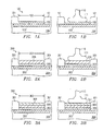
- FIG. 1A shows a schematic cross section of the first embodiment of the invention, generally designated 100.
- An integrated circuit IC
- This overcoat is usually made of silicon nitride, commonly 500 to 1000 nm thick.
- a window 102 is opened in the overcoat in order to expose portion of the copper metallization 103.
- the underlayer embedding the copper and preventing its diffusion into parts of the IC (usually made of tantalum nitride, tantalum silicon nitride, tungsten nitride, tungsten silicon nitride, titanium, titanium nitride, or titanium tungsten).
- the dielectric IC portions 104 are only summarily indicated.
- These electrically insulating portions may include not only the traditional plasma-enhanced chemical vapor deposited dielectrics such as silicon dioxide, but also newer dielectric materials having lower dielectric constants, such as silicon-containing hydrogen silsesquioxane, organic polyimides, aerogels, and parylenes, or stacks of dielectric layers including plasma-generated or ozone tetraethylorthosilicate oxide. Since these materials are less dense and mechanically weaker than the previous standard insulators, the dielectric under the copper is often reinforced. Examples can be found in U.S.
- Patent applications # 60/085,876, filed on 05/18/98 (Saran et al., “Fine Pitch System and Method for Reinforcing Bond Pads in Semiconductors"), and # 60/092,961, filed 07/14/98 (Saran, “System and Method for Bonding over Active Integrated Circuits”).
- the present invention provides structures and processes of a cap formed over the exposed copper, as described in FIGs. 1, 2 and 3.
- the cap consists of a metal and has a coordinated thickness such that it satisfies three requirements:
- wire ball bonding is the preferred method of using coupling members to create electrical connections.
- Another method is ribbon bonding employing wedge bonders.
- wedge bonding ball bonding operates at elevated temperatures for which the materials and processes of this invention need to be harmonized.
- the wire bonding process begins by positioning both the IC chip with the bond pads and the object, to which the chip is to be bonded, on a heated pedestal to raise their temperature to between 170 and 300 °C.
- a wire 110 (in FIGs. 1B, 2B, and 3B), typically of gold, gold-beryllium alloy, other gold alloy, copper, aluminum, or alloys thereof, having a diameter typically ranging from 18 to 33 ⁇ m, is strung through a heated capillary where the temperature usually ranges between 200 and 500 °C.
- a free air ball is created using either a flame or a spark technique.
- the ball has a typical diameter from about 1.2 to 1.6 wire diameters.
- the capillary is moved towards the chip bonding pad (102 in FIG.
- Ball pitches as small as between 75 and 40 ⁇ m can be achieved.
- Such advances can, for instance, be found in the computerized bonder 8020 by Kulicke & Soffa, Willow Grove, PA, U.S.A., or in the ABACUS SA by Texas Instruments, Dallas, TX, U.S.A. Moving the capillary in a predetermined and computer-controlled manner through the air will create a wire looping of exactly defined shape. Finally, the capillary reaches its desired destination and is lowered to touch the contact pad of the object.
- barrier cap metals 103 in FIGs. 1A and 1B are platinum, rhodium, iridium, and osmium.
- copper has a diffusion coefficient of less than 1 x 10E-23 cm 2 /s at 250 °C. Consequently, these metals are good copper diffusion barriers.
- the layer thicknesses required to reduce copper diffusion by more than 80 % compared to the absence of the layers are obtained by diffusion calculations.
- the Table of the Appendix lists the layer thickness of platinum when copper is diffusing at 250 °C or 160 °C, with diffusion time (min) as parameter.
- a barrier thickness from about 0.5 to 1.5 ⁇ m will safely meet the copper reduction criterion.
- the metals quoted above can be deposited by electroless plating (more detail about this technique below). Furthermore, these metals are bondable. A drawback, however, of the metals quoted is their high cost.
- a lower cost solution is offered by the second embodiment of the invention, generally designated 200 in FIG. 2A.
- 201 indicates the protective overcoat defining the size 202 of the bond pad.
- 203 is the copper metallization of the bond pad, and 204 the underlying dielectric material.
- the metal cap over the copper 203 is provided by two layers:
- Layer 205 is positioned over copper 203, sometimes deposited on a seed metal layer (see FIG. 4).
- Examples for layer 205 are nickel, cobalt, chromium, molybdenum, titanium, tungsten, and alloys thereof. These metals are inexpensive and can be deposited by electroless plating; however, they are poorly bondable. In these metals, copper has a diffusion coefficient of less than 1 X 10E-23 cm 2 /s at 250 °C. Consequently, these metals are good copper diffusion barriers. The layer thicknesses required to reduce copper diffusion by more than 80 % compared to the absence of the layers are obtained by diffusion calculations.
- the Table of the Appendix lists the layer thickness of nickel when copper is diffusing at 250 °C or 160 °C, with diffusion time (min) as parameter.
- a barrier thickness from about 0.5 to 1.5 ⁇ m will safely meet the copper reduction criterion.
- Layer 206 is positioned over layer 205 as the outermost layer of the cap; they are bondable so that they can accept the wire bond 111.
- Examples for layer 206 are gold, platinum, palladium, and silver.
- these metals have a diffusion coefficient for the metals used in barrier 205 (such as nickel) of less than 1 x 10E-14 cm 2 /s at 250 °C. Consequently, these metals are good diffusion barriers for the materials of layer 205.
- the layer thicknesses required to reduce the up-diffusion of metal used in layer 205 by more than 80 % compared to the absence of layer 206 are obtained from diffusion calculations.
- the Table of the Appendix lists the layer thickness ( ⁇ m) of gold when nickel is up-diffusing at 250 °C or 160 °C, with diffusion time (min) as parameter. Generally an outermost layer thickness of 1.5 ⁇ m or somewhat less will safely meet the reduction criterion for metal diffusing from layer 205.
- the third embodiment is generally designated 300 in FIG. 3A; 301 indicates the protective overcoat defining the size 302 of the bond pad.
- 303 is the copper metallization of the bond pad, and 304 the underlying dielectric material.
- the metal cap over the copper 303 is provided by three layers:
- Layer 305 is positioned over copper area 303, sometimes deposited on a seed metal layer (not shown in FIG. 3A and 3B, but see FIG. 4).
- Layer 305 consists of a metal acting as a diffusion barrier against copper.
- Examples for layer 305 are nickel, cobalt, chromium, molybdenum, titanium, tungsten, and alloys thereof. These metals are inexpensive and can be deposited by electroless plating; however, they are poorly bondable.
- copper has a diffusion coefficient of less than 1 x 10E-23 cm 2 /s at 250 °C. Consequently, these metals are good copper diffusion barriers.
- the layer thicknesses required to reduce copper diffusion by more than 80 % compared to the absence of the layers, are obtained by diffusion calculations.
- the Table of the Appendix lists the layer thickness of nickel when copper is diffusing at 250 °C or 160 °C, with diffusion time (min) as parameter.
- a barrier thickness from about 0.5 to 1.5 ⁇ m will safely meet the copper reduction criterion.
- Layer 306 is positioned over layer 305 as an effective diffusion barrier against the up-diffusing metal used in layer 305.
- the intent is to de-emphasize the barrier function of the outermost layer 307, and rather emphasize its bondability function. Consequently, the thickness required for the outermost layer 307 can be reduced, thus saving cost.
- Examples for layer 306 are palladium, cobalt, platinum, and osmium.
- Examples for layer 307 are gold, platinum, and silver.
- Metals used for layer 306 have a diffusion coefficient for the metals used in barrier layer 305 (such as nickel) of less than 1 x 10E-14 cm 2 /s at 250 °C.
- the layer thicknesses required to reduce the up-diffusion of metal used in layer 305 by more than 80 % compared to the absence of layer 306 are obtained from diffusion calculations.
- the Table of the Appendix lists the layer thickness ( ⁇ m) of palladium when nickel is up-diffusing at 250 °C or 160 °C, with diffusion time (min) as parameter.
- a thickness of layer 305 of about 0.4 to 1.5 ⁇ m will safely meet the reduction criterion for metal diffusing from layer 305.
- the thickness of the bondable outermost layer 307 (such as gold) can now be reduced to the range of about 0.02 to 0.1 ⁇ m.
- FIG. 4 summarizes the third embodiment of the present invention in more detail; most dimension ranges are quoted in FIGs. 1 to 3, and the electroless plating and other fabrication process steps are discussed in FIG. 5.
- the protective overcoat 401 has an opening, defining the size of the bond pad, and a thickness sufficient to accommodate most of the stacked layers, which cap the bond pad IC copper metallization 403.
- the copper trace 403 is imbedded in refractory metal shield 402 (for example, tantalum nitride), which is surrounded by dielectric 404 (re-enforcement methods see above).
- the first layer of the cap Directly facing the cleaned and non-oxidized copper surface 403a is the first layer of the cap, a thin layer 408 of seed metal (for example, palladium, about 5 to 10 nm thick; another choice is tin).
- seed metal for example, palladium, about 5 to 10 nm thick; another choice is tin.
- metal layer 405 for example, nickel
- metal layer 406 for example, palladium
- the outermost layer of the cap is metal layer 707 (for example, gold), which is metallurgically bonded by wire "ball" 411. As FIG. 4 shows, the electroless plating process may deposit some metal of the layers onto the protective overcoat beyond the periphery 401a of the bond pad opening.
- metal layer 707 for example, gold
- the electroless process used for fabricating the bond pad cap of FIG. 4 is detailed in FIG. 5. After the bond pads have been opened in the protective overcoat, exposing the copper IC metallization in bond pad areas, the cap deposition process starts at 501; the sequence of process steps is as follows:
- the invention can be applied to IC bond pad metallizations other than copper, which are difficult or impossible to bond by conventional ball or wedge bonding techniques, such as alloys of refractory metals and noble metals.
- the invention can be extended to batch processing, further reducing fabrication costs.
- the invention can be used in hybrid technologies of wire/ribbon bonding and solder interconnections.
Landscapes
- Wire Bonding (AREA)
- Internal Circuitry In Semiconductor Integrated Circuit Devices (AREA)
Applications Claiming Priority (4)
| Application Number | Priority Date | Filing Date | Title |
|---|---|---|---|
| US18340500P | 2000-02-18 | 2000-02-18 | |
| US183405P | 2000-02-18 | ||
| US19194900P | 2000-03-24 | 2000-03-24 | |
| US191949P | 2000-03-24 |
Publications (2)
| Publication Number | Publication Date |
|---|---|
| EP1126519A2 true EP1126519A2 (de) | 2001-08-22 |
| EP1126519A3 EP1126519A3 (de) | 2004-02-18 |
Family
ID=26879086
Family Applications (1)
| Application Number | Title | Priority Date | Filing Date |
|---|---|---|---|
| EP01000021A Withdrawn EP1126519A3 (de) | 2000-02-18 | 2001-02-19 | Struktur und Herstellungsmethode von Anschlussflächen auf verkupferten intergrierten Schaltungen |
Country Status (5)
| Country | Link |
|---|---|
| EP (1) | EP1126519A3 (de) |
| JP (1) | JP2001267357A (de) |
| KR (1) | KR20010082730A (de) |
| CN (1) | CN1314225A (de) |
| TW (1) | TW494510B (de) |
Cited By (7)
| Publication number | Priority date | Publication date | Assignee | Title |
|---|---|---|---|---|
| WO2003025998A3 (en) * | 2001-09-14 | 2003-06-12 | Motorola Inc | Method of forming a bond pad and structure thereof |
| US6933614B2 (en) | 2003-04-02 | 2005-08-23 | Freescale Semiconductor, Inc. | Integrated circuit die having a copper contact and method therefor |
| DE102006022444A1 (de) * | 2006-05-13 | 2007-11-15 | Conti Temic Microelectronic Gmbh | Mikrostrukturierter elektronischer Baustein |
| EP2177646A1 (de) | 2008-10-17 | 2010-04-21 | Atotech Deutschland Gmbh | Spannungsreduzierte Ni-P/Pd-Stapel für Waferoberfläche |
| EP2273544A3 (de) * | 2001-12-14 | 2011-10-26 | STMicroelectronics S.r.l. | Elektronische Halbleitervorrichtung und Verfahren zu deren Herstellung |
| US8399989B2 (en) | 2005-07-29 | 2013-03-19 | Megica Corporation | Metal pad or metal bump over pad exposed by passivation layer |
| WO2020094642A1 (en) | 2018-11-06 | 2020-05-14 | Atotech Deutschland Gmbh | Electroless nickel plating solution |
Families Citing this family (26)
| Publication number | Priority date | Publication date | Assignee | Title |
|---|---|---|---|---|
| US8110489B2 (en) | 2001-07-25 | 2012-02-07 | Applied Materials, Inc. | Process for forming cobalt-containing materials |
| US9051641B2 (en) * | 2001-07-25 | 2015-06-09 | Applied Materials, Inc. | Cobalt deposition on barrier surfaces |
| DE10156054C2 (de) * | 2001-11-15 | 2003-11-13 | Infineon Technologies Ag | Herstellungsverfahren für eine Leiterbahn auf einem Substrat |
| JP3820975B2 (ja) * | 2001-12-12 | 2006-09-13 | ソニー株式会社 | 半導体装置及びその製造方法 |
| JP4170103B2 (ja) * | 2003-01-30 | 2008-10-22 | Necエレクトロニクス株式会社 | 半導体装置、および半導体装置の製造方法 |
| US7268074B2 (en) * | 2004-06-14 | 2007-09-11 | Enthone, Inc. | Capping of metal interconnects in integrated circuit electronic devices |
| JP4674522B2 (ja) * | 2004-11-11 | 2011-04-20 | 株式会社デンソー | 半導体装置 |
| WO2006059578A1 (ja) * | 2004-12-03 | 2006-06-08 | Murata Manufacturing Co., Ltd. | 電気接点部品、同軸コネクタおよびそれらを用いた電気回路装置 |
| US7649614B2 (en) * | 2005-06-10 | 2010-01-19 | Asml Netherlands B.V. | Method of characterization, method of characterizing a process operation, and device manufacturing method |
| US8148822B2 (en) | 2005-07-29 | 2012-04-03 | Megica Corporation | Bonding pad on IC substrate and method for making the same |
| CN1905176B (zh) * | 2005-07-29 | 2010-10-20 | 米辑电子股份有限公司 | 线路组件结构及其制作方法 |
| JP4793006B2 (ja) * | 2006-02-09 | 2011-10-12 | ソニー株式会社 | 半導体装置及びその製造方法 |
| EP2023384A4 (de) * | 2006-05-29 | 2013-01-02 | Nec Corp | Elektronische komponente, halbleiterkapselung und elektronische anordnung |
| JP5293185B2 (ja) * | 2006-09-26 | 2013-09-18 | 日立金属株式会社 | 電子部品の製造方法 |
| JP2010171386A (ja) * | 2008-12-26 | 2010-08-05 | Sanyo Electric Co Ltd | 半導体装置及びその製造方法 |
| SG182432A1 (en) * | 2010-01-27 | 2012-08-30 | Sumitomo Bakelite Co | Semiconductor device |
| JP5471882B2 (ja) * | 2010-06-24 | 2014-04-16 | 日亜化学工業株式会社 | 半導体素子 |
| JP2012069691A (ja) * | 2010-09-22 | 2012-04-05 | Toshiba Corp | 半導体装置とその製造方法 |
| JP2013004781A (ja) * | 2011-06-17 | 2013-01-07 | Sanken Electric Co Ltd | 半導体装置及び半導体装置の製造方法 |
| CN102915981B (zh) * | 2012-11-08 | 2016-02-03 | 南通富士通微电子股份有限公司 | 半导体器件及其封装方法 |
| CN103151280B (zh) * | 2013-03-04 | 2015-07-22 | 哈尔滨工业大学(威海) | 一种金丝与铜箔的连接方法 |
| JP6607771B2 (ja) * | 2015-12-03 | 2019-11-20 | ローム株式会社 | 半導体装置 |
| JP6937283B2 (ja) * | 2018-09-19 | 2021-09-22 | 株式会社東芝 | 半導体装置の製造方法 |
| JP2020194875A (ja) * | 2019-05-28 | 2020-12-03 | 京セラ株式会社 | 配線基板およびそれを用いた電子部品実装構造体 |
| CN112216675A (zh) * | 2020-09-11 | 2021-01-12 | 中国电子科技集团公司第十三研究所 | 微组装基板结构及芯片微组装方法 |
| CN115623671A (zh) * | 2021-07-13 | 2023-01-17 | 长鑫存储技术有限公司 | 电路板结构、半导体结构及半导体结构的制作方法 |
Family Cites Families (10)
| Publication number | Priority date | Publication date | Assignee | Title |
|---|---|---|---|---|
| US4463059A (en) * | 1982-06-30 | 1984-07-31 | International Business Machines Corporation | Layered metal film structures for LSI chip carriers adapted for solder bonding and wire bonding |
| US4985310A (en) * | 1988-04-08 | 1991-01-15 | International Business Machines Corp. | Multilayered metallurgical structure for an electronic component |
| KR940010510B1 (ko) * | 1988-11-21 | 1994-10-24 | 세이꼬 엡슨 가부시끼가이샤 | 반도체 장치 제조 방법 |
| US5367195A (en) * | 1993-01-08 | 1994-11-22 | International Business Machines Corporation | Structure and method for a superbarrier to prevent diffusion between a noble and a non-noble metal |
| JP2783133B2 (ja) * | 1993-09-29 | 1998-08-06 | 松下電器産業株式会社 | ワイヤボンディング前処理方法 |
| US5567657A (en) * | 1995-12-04 | 1996-10-22 | General Electric Company | Fabrication and structures of two-sided molded circuit modules with flexible interconnect layers |
| US5969424A (en) * | 1997-03-19 | 1999-10-19 | Fujitsu Limited | Semiconductor device with pad structure |
| DE69838586T2 (de) * | 1997-06-04 | 2008-07-24 | Ibiden Co., Ltd., Ogaki | Lötelement für gedruckte leiterplatten |
| JP3436102B2 (ja) * | 1997-09-25 | 2003-08-11 | イビデン株式会社 | 半田材料並びにプリント配線板及びその製造方法 |
| US5910644A (en) * | 1997-06-11 | 1999-06-08 | International Business Machines Corporation | Universal surface finish for DCA, SMT and pad on pad interconnections |
-
2001
- 2001-02-16 CN CN01111396A patent/CN1314225A/zh active Pending
- 2001-02-17 KR KR1020010007981A patent/KR20010082730A/ko not_active Withdrawn
- 2001-02-19 EP EP01000021A patent/EP1126519A3/de not_active Withdrawn
- 2001-02-19 JP JP2001041939A patent/JP2001267357A/ja active Pending
- 2001-03-14 TW TW090103495A patent/TW494510B/zh not_active IP Right Cessation
Cited By (9)
| Publication number | Priority date | Publication date | Assignee | Title |
|---|---|---|---|---|
| WO2003025998A3 (en) * | 2001-09-14 | 2003-06-12 | Motorola Inc | Method of forming a bond pad and structure thereof |
| EP2273544A3 (de) * | 2001-12-14 | 2011-10-26 | STMicroelectronics S.r.l. | Elektronische Halbleitervorrichtung und Verfahren zu deren Herstellung |
| EP2306503A3 (de) * | 2001-12-14 | 2011-11-02 | STMicroelectronics Srl | Elektronische Halbleitervorrichtung und Verfahren zu deren Herstellung |
| US6933614B2 (en) | 2003-04-02 | 2005-08-23 | Freescale Semiconductor, Inc. | Integrated circuit die having a copper contact and method therefor |
| US8399989B2 (en) | 2005-07-29 | 2013-03-19 | Megica Corporation | Metal pad or metal bump over pad exposed by passivation layer |
| DE102006022444A1 (de) * | 2006-05-13 | 2007-11-15 | Conti Temic Microelectronic Gmbh | Mikrostrukturierter elektronischer Baustein |
| EP2177646A1 (de) | 2008-10-17 | 2010-04-21 | Atotech Deutschland Gmbh | Spannungsreduzierte Ni-P/Pd-Stapel für Waferoberfläche |
| US8986789B2 (en) | 2008-10-17 | 2015-03-24 | Atotech Deutschland Gmbh | Stress-reduced Ni-P/Pd stacks for bondable wafer surfaces |
| WO2020094642A1 (en) | 2018-11-06 | 2020-05-14 | Atotech Deutschland Gmbh | Electroless nickel plating solution |
Also Published As
| Publication number | Publication date |
|---|---|
| EP1126519A3 (de) | 2004-02-18 |
| JP2001267357A (ja) | 2001-09-28 |
| TW494510B (en) | 2002-07-11 |
| KR20010082730A (ko) | 2001-08-30 |
| CN1314225A (zh) | 2001-09-26 |
Similar Documents
| Publication | Publication Date | Title |
|---|---|---|
| US6800555B2 (en) | Wire bonding process for copper-metallized integrated circuits | |
| EP1126519A2 (de) | Struktur und Herstellungsmethode von Anschlussflächen auf verkupferten intergrierten Schaltungen | |
| US20010033020A1 (en) | Structure and method for bond pads of copper-metallized integrated circuits | |
| US7045903B2 (en) | Integrated power circuits with distributed bonding and current flow | |
| US6384486B2 (en) | Bonding over integrated circuits | |
| JP3737482B2 (ja) | 自己不動態化Cu合金を用いて接着されたCuパッド/Cuワイヤ | |
| CN1269212C (zh) | 将电路和引线框的功率分布功能集成到芯片表面上的电路结构 | |
| KR101339517B1 (ko) | 알루미늄 구리 본드 패드를 위한 캡 층 | |
| US6435398B2 (en) | Method for chemically reworking metal layers on integrated circuit bond pads | |
| US20080274294A1 (en) | Copper-metallized integrated circuits having electroless thick copper bond pads | |
| US7351651B2 (en) | Structure and method for contact pads having a recessed bondable metal plug over of copper-metallized integrated circuits | |
| US20050215048A1 (en) | Structure and method for contact pads having an overcoat-protected bondable metal plug over copper-metallized integrated circuits | |
| US6534327B2 (en) | Method for reworking metal layers on integrated circuit bond pads | |
| WO2008061128A2 (en) | Copper-metallized integrated circuits having an overcoat for protecting bondable metal contacts and improving mold compound adhesion | |
| US6619538B1 (en) | Nickel plating process having controlled hydrogen concentration | |
| WO2005062367A1 (en) | I/o sites for probe test and wire bond | |
| KR20070022032A (ko) | 구리-금속화 집적 회로 위에 오버코트-보호된 본딩 가능한금속 플러그를 갖는 콘택트 패드를 위한 구조 및 방법 |
Legal Events
| Date | Code | Title | Description |
|---|---|---|---|
| PUAI | Public reference made under article 153(3) epc to a published international application that has entered the european phase |
Free format text: ORIGINAL CODE: 0009012 |
|
| AK | Designated contracting states |
Kind code of ref document: A2 Designated state(s): AT BE CH CY DE DK ES FI FR GB GR IE IT LI LU MC NL PT SE TR |
|
| AX | Request for extension of the european patent |
Free format text: AL;LT;LV;MK;RO;SI |
|
| PUAL | Search report despatched |
Free format text: ORIGINAL CODE: 0009013 |
|
| AK | Designated contracting states |
Kind code of ref document: A3 Designated state(s): AT BE CH CY DE DK ES FI FR GB GR IE IT LI LU MC NL PT SE TR |
|
| AX | Request for extension of the european patent |
Extension state: AL LT LV MK RO SI |
|
| 17P | Request for examination filed |
Effective date: 20040818 |
|
| 17Q | First examination report despatched |
Effective date: 20040923 |
|
| AKX | Designation fees paid |
Designated state(s): DE FR GB |
|
| RBV | Designated contracting states (corrected) |
Designated state(s): AT BE CH CY DE DK ES FI FR GB GR IE IT LI LU MC NL PT SE TR |
|
| STAA | Information on the status of an ep patent application or granted ep patent |
Free format text: STATUS: THE APPLICATION IS DEEMED TO BE WITHDRAWN |
|
| 18D | Application deemed to be withdrawn |
Effective date: 20050405 |