EP1128217B1 - Méthode de mesure des aberrations dans un système optique de formation d'image - Google Patents
Méthode de mesure des aberrations dans un système optique de formation d'image Download PDFInfo
- Publication number
- EP1128217B1 EP1128217B1 EP01301571A EP01301571A EP1128217B1 EP 1128217 B1 EP1128217 B1 EP 1128217B1 EP 01301571 A EP01301571 A EP 01301571A EP 01301571 A EP01301571 A EP 01301571A EP 1128217 B1 EP1128217 B1 EP 1128217B1
- Authority
- EP
- European Patent Office
- Prior art keywords
- radiation
- projection
- settings
- parameter
- coefficient
- Prior art date
- Legal status (The legal status is an assumption and is not a legal conclusion. Google has not performed a legal analysis and makes no representation as to the accuracy of the status listed.)
- Expired - Lifetime
Links
- 230000004075 alteration Effects 0.000 title claims description 65
- 238000000034 method Methods 0.000 title claims description 58
- 238000012634 optical imaging Methods 0.000 title claims description 3
- 230000005855 radiation Effects 0.000 claims description 58
- 238000005286 illumination Methods 0.000 claims description 57
- 239000000758 substrate Substances 0.000 claims description 42
- 238000005259 measurement Methods 0.000 claims description 23
- 238000000059 patterning Methods 0.000 claims description 22
- 238000003384 imaging method Methods 0.000 claims description 13
- 210000001747 pupil Anatomy 0.000 claims description 9
- 238000012937 correction Methods 0.000 claims description 8
- 230000008859 change Effects 0.000 claims description 7
- 238000004519 manufacturing process Methods 0.000 claims description 7
- 239000000463 material Substances 0.000 claims description 7
- 238000004364 calculation method Methods 0.000 claims description 4
- 230000006870 function Effects 0.000 description 21
- 239000010410 layer Substances 0.000 description 12
- 235000012431 wafers Nutrition 0.000 description 12
- 206010010071 Coma Diseases 0.000 description 7
- 201000009310 astigmatism Diseases 0.000 description 6
- 230000005540 biological transmission Effects 0.000 description 5
- 238000009826 distribution Methods 0.000 description 5
- 230000000694 effects Effects 0.000 description 5
- 239000011159 matrix material Substances 0.000 description 4
- 238000000691 measurement method Methods 0.000 description 4
- 230000010363 phase shift Effects 0.000 description 4
- 230000008569 process Effects 0.000 description 4
- 238000012360 testing method Methods 0.000 description 4
- 238000004088 simulation Methods 0.000 description 3
- XUIMIQQOPSSXEZ-UHFFFAOYSA-N Silicon Chemical compound [Si] XUIMIQQOPSSXEZ-UHFFFAOYSA-N 0.000 description 2
- 230000002238 attenuated effect Effects 0.000 description 2
- 230000008901 benefit Effects 0.000 description 2
- 230000001419 dependent effect Effects 0.000 description 2
- 238000012545 processing Methods 0.000 description 2
- 230000011218 segmentation Effects 0.000 description 2
- 229910052710 silicon Inorganic materials 0.000 description 2
- 239000010703 silicon Substances 0.000 description 2
- 101000634119 Arabidopsis thaliana RNA polymerase sigma factor sigC Proteins 0.000 description 1
- 229910001374 Invar Inorganic materials 0.000 description 1
- 230000032683 aging Effects 0.000 description 1
- 238000003491 array Methods 0.000 description 1
- 239000011248 coating agent Substances 0.000 description 1
- 238000000576 coating method Methods 0.000 description 1
- 230000003750 conditioning effect Effects 0.000 description 1
- 238000012790 confirmation Methods 0.000 description 1
- 238000010276 construction Methods 0.000 description 1
- 238000013461 design Methods 0.000 description 1
- 238000001514 detection method Methods 0.000 description 1
- 238000011161 development Methods 0.000 description 1
- 230000018109 developmental process Effects 0.000 description 1
- 230000005670 electromagnetic radiation Effects 0.000 description 1
- 238000005530 etching Methods 0.000 description 1
- 230000004907 flux Effects 0.000 description 1
- 238000010438 heat treatment Methods 0.000 description 1
- 238000011065 in-situ storage Methods 0.000 description 1
- 238000007689 inspection Methods 0.000 description 1
- 238000005305 interferometry Methods 0.000 description 1
- 238000005468 ion implantation Methods 0.000 description 1
- 239000002346 layers by function Substances 0.000 description 1
- 239000004973 liquid crystal related substance Substances 0.000 description 1
- 238000001459 lithography Methods 0.000 description 1
- 230000005381 magnetic domain Effects 0.000 description 1
- 238000013507 mapping Methods 0.000 description 1
- 230000015654 memory Effects 0.000 description 1
- QSHDDOUJBYECFT-UHFFFAOYSA-N mercury Chemical compound [Hg] QSHDDOUJBYECFT-UHFFFAOYSA-N 0.000 description 1
- 229910052753 mercury Inorganic materials 0.000 description 1
- 238000001465 metallisation Methods 0.000 description 1
- 230000003287 optical effect Effects 0.000 description 1
- 230000003647 oxidation Effects 0.000 description 1
- 238000007254 oxidation reaction Methods 0.000 description 1
- 238000000206 photolithography Methods 0.000 description 1
- 238000005498 polishing Methods 0.000 description 1
- 230000037452 priming Effects 0.000 description 1
- 230000002441 reversible effect Effects 0.000 description 1
- 239000004065 semiconductor Substances 0.000 description 1
- 238000007493 shaping process Methods 0.000 description 1
- 238000010008 shearing Methods 0.000 description 1
- 239000007787 solid Substances 0.000 description 1
- 239000010409 thin film Substances 0.000 description 1
- 230000004304 visual acuity Effects 0.000 description 1
Images



Classifications
-
- G—PHYSICS
- G03—PHOTOGRAPHY; CINEMATOGRAPHY; ANALOGOUS TECHNIQUES USING WAVES OTHER THAN OPTICAL WAVES; ELECTROGRAPHY; HOLOGRAPHY
- G03F—PHOTOMECHANICAL PRODUCTION OF TEXTURED OR PATTERNED SURFACES, e.g. FOR PRINTING, FOR PROCESSING OF SEMICONDUCTOR DEVICES; MATERIALS THEREFOR; ORIGINALS THEREFOR; APPARATUS SPECIALLY ADAPTED THEREFOR
- G03F7/00—Photomechanical, e.g. photolithographic, production of textured or patterned surfaces, e.g. printing surfaces; Materials therefor, e.g. comprising photoresists; Apparatus specially adapted therefor
- G03F7/70—Microphotolithographic exposure; Apparatus therefor
- G03F7/70483—Information management; Active and passive control; Testing; Wafer monitoring, e.g. pattern monitoring
- G03F7/70591—Testing optical components
- G03F7/706—Aberration measurement
Definitions
- the present invention relates to a method of measuring aberration in an optical imaging system, such as a lithographic projection apparatus. Observations are made as a function of parameters of the projection apparatus, and from these the presence of different types of aberration can be quantified.
- the lithographic projection apparatus may comprise:
- the patterning means here referred to should be broadly interpreted as referring to means that can be used to endow an incoming radiation beam with a patterned cross-section, corresponding to a pattern that is to be created in a target portion of the substrate; the term "light valve" can also be used in this context.
- the said pattern will correspond to a particular functional layer in a device being created in the target portion, such as an integrated circuit or other device (see below). Examples of such patterning means include:
- Lithographic projection apparatus can be used, for example, in the manufacture of integrated circuits (ICs).
- the patterning means may generate a circuit pattern corresponding to an individual layer of the IC, and this pattern can be imaged onto a target portion (e.g . comprising one or more dies) on a substrate (silicon wafer) that has been coated with a layer of radiation-sensitive material (resist).
- a target portion e.g . comprising one or more dies
- a substrate silicon wafer
- a layer of radiation-sensitive material resist
- a single wafer will contain a whole network of adjacent target portions that are successively irradiated via the projection system, one at a time.
- employing patterning by a mask on a mask table a distinction can be made between two different types of machine.
- each target portion is irradiated by exposing the entire mask pattern onto the target portion in one go; such an apparatus is commonly referred to as a wafer stepper.
- a step-and-scan apparatus each target portion is irradiated by progressively scanning the mask pattern under the projection beam in a given reference direction (the "scanning" direction) while synchronously scanning the substrate table parallel or anti-parallel to this direction; since, in general, the projection system will have a magnification factor M (generally ⁇ 1), the speed V at which the substrate table is scanned will be a factor M times that at which the mask table is scanned. More information with regard to lithographic devices as here described can be gleaned, for example, from US 6,046,792 .
- a pattern (e.g. in a mask) is imaged onto a substrate that is at least partially covered by a layer of radiation-sensitive material (resist).
- the substrate Prior to this imaging step, the substrate may undergo various procedures, such as priming, resist coating and a soft bake. After exposure, the substrate may be subjected to other procedures, such as a post-exposure bake (PEB), development, a hard bake and measurement/inspection of the imaged features.
- PEB post-exposure bake
- This array of procedures is used as a basis to pattern an individual layer of a device, e.g. an IC.
- Such a patterned layer may then undergo various processes such as etching, ion-implantation (doping), metallization, oxidation, chemo-mechanical polishing, etc., all intended to finish off an individual layer. If several layers are required, then the whole procedure, or a variant thereof, will have to be repeated for each new layer. Eventually, an array of devices will be present on the substrate (wafer). These devices are then separated from one another by a technique such as dicing or sawing, whence the individual devices can be mounted on a carrier, connected to pins, etc. Further information regarding such processes can be obtained, for example, from the book " Microchip Fabrication: A Practical Guide to Semiconductor Processing", Third Edition, by Peter van Zant, McGraw Hill Publishing Co., 1997, ISBN 0-07-067250-4 .
- the projection system may hereinafter be referred to as the "lens"; however, this term should be broadly interpreted as encompassing various types of projection system, including refractive optics, reflective optics, and catadioptric systems, for example.
- the radiation system may also include components operating according to any of these design types for directing, shaping or controlling the projection beam of radiation, and such components may also be referred to below, collectively or singularly, as a "lens".
- the lithographic apparatus may be of a type having two or more substrate tables (and/or two or more mask tables). In such "multiple stage” devices the additional tables may be used in parallel, or preparatory steps may be carried out on one or more tables while one or more other tables are being used for exposures. Twin stage lithographic apparatus are described, for example, in US 5,969,441 and WO 98/40791 .
- the projection system (“lens”) is thus not an ideal, diffraction-limited system, but an aberration-limited system.
- the aberrations are dependent on position in the image field and are an important source of variations in the imaged line widths occurring across the image field, as well as influencing the focus, exposure latitude and so on. They also cause field-dependent overlay errors between different mask structures and/or different illumination settings.
- the influence of aberrations becomes increasingly significant with the application of newer techniques, such as phase-shift masks or off-axis illumination, to enhance the resolving power of a lithographic projection apparatus.
- a further problem is that the aberrations are not constant in modern lithographic projection systems.
- these projection systems In order to minimise low-order aberrations, such as distortion, curvature of field, astigmatism, coma and spherical aberration, these projection systems generally comprise one or more movable elements.
- the wavelengths of the projection beam or the position of the mask table may be adjustable for the same purpose. When these adjusting facilities are used, other, smaller aberrations may be introduced.
- the intensity of the projection beam must be as large as possible, the components of the projection system are subject to ageing so that the aberrations may change during the lifetime of the apparatus.
- reversible changes e.g. as caused by lens heating, may temporarily change the aberrations.
- the present invention provides a method of determining aberration of an optical imaging system comprising:
- said plurality of different settings comprise different numerical aperture settings and/or sigma settings, illumination modes or telecentricitv modes furthermore, one may use various types and sizes of test structures on, for instance, one or more masks, to create different diffraction effects in the projection system. All such variation should be interpreted as falling within the meaning of the phrase "different illumination settings” as used in this text.
- the term "sigma ( ⁇ ) setting” refers to the radial extent of the intensity distribution in the beam at a pupil in the imaging system through which the radiation passes, normalized with respect to the maximum radius of the pupil. Thus, a sigma value of 1 represents an illumination intensity distribution with a radius at the pupil equal to the maximum radius of the pupil.
- illumination mode denotes the spatial distribution of the radiation at the pupil, which may be, for example, disc-shaped, annular (which would be characterized by sigma inner and sigma outer settings), quadrupolar, dipolar, soft-multipolar (including some radiation flux in between the poles), etc.
- telecentricity modes encompasses configuring the imaging system telecentrically and/or with varying degrees of non-telecentricity, for example by the use of prisms on top of a mask to tilt the illumination profile. These different settings can be selected conveniently in a lithographic projection apparatus.
- the measured parameter can be one or more of: the position of best-focus of said image; the lateral position of said image; the deformation of said image; and other properties of exposing said image lithographically, such as line width and shape, and distance between adjacent structures.
- the plurality of different settings are selected such that the variation in the or each at least one measured parameter is substantially maximized. In this way the accuracy of the determined coefficient(s) can be improved.
- the plurality of different settings are selected such that the variation in said at least one measured parameter resulting from aberration represented by one or more of said coefficients is substantially zero, whilst the variation in said at least one parameter as the function of a coefficient that is to be determined, is non-zero.
- This technique enables different aberration coefficients, such as Zernike coefficients, to be obtained independently of each other.
- the invention also provides a lithographic projection apparatus for projecting a patterned beam of radiation onto a substrate provided with a radiation-sensitive layer, the apparatus comprising:
- a device manufacturing method comprising the steps of:
- the terms "radiation” and “beam” are used to encompass all types of electromagnetic radiation, including ultraviolet radiation (e . g . with a wavelength of 365, 248, 193, 157 or 126 nm) and EUV (extreme ultra-violet radiation, e.g. having a wavelength in the range 5-20 nm).
- Figure 1 schematically depicts a lithographic projection apparatus according to a particular embodiment of the invention.
- the apparatus comprises:
- the source LA (e.g . a Hg lamp or an excimer laser) produces a beam of radiation.
- This beam is fed into an illumination system (illuminator) IL, either directly or after having traversed conditioning means, such as a beam expander Ex, for example.
- the illuminator IL may comprise adjusting means AM for setting the ⁇ -outer and ⁇ -inner values of the intensity distribution in the beam.
- it will generally comprise various other components, such as an integrator IN and a condenser CO. In this way, the beam PB impinging on the mask MA has a desired uniformity and intensity distribution in its cross-section.
- the source LA may be within the housing of the lithographic projection apparatus (as is often the case when the source LA is a mercury lamp, for example), but that it may also be remote from the lithographic projection apparatus, the radiation beam which it produces being led into the apparatus (e.g. with the aid of suitable directing mirrors); this latter scenario is often the case when the source LA is an excimer laser.
- the current invention and Claims encompass both of these scenarios.
- the beam PB subsequently intercepts the mask MA, which is held on a mask table MT. Having traversed the mask MA, the beam PB passes through the lens PL, which focuses the beam PB onto a target portion C of the substrate W. With the aid of the second positioning means (and interferometric measuring means IF), the substrate table WT can be moved accurately, e.g. so as to position different target portions C in the path of the beam PB. Similarly, the first positioning means can be used to accurately position the mask MA with respect to the path of the beam PB, e . g . after mechanical retrieval of the mask MA from a mask library, or during a scan.
- the mask table MT may just be connected to a short stroke actuator, or may be fixed.
- the depicted apparatus can be used in two different modes:
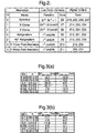
- Figures 3(a) and 3(b) are tables giving the results of these calculations for two different lithographic projection apparatuses. The first two columns give the settings of the illumination mode in terms of the numerical aperture (NA), on the image side, and the sigma ( ⁇ ) setting.
- NA numerical aperture
- ⁇ sigma
- the illumination modes used in the tables of Figures 3(a) and 3(b) are annular illumination modes, and the two values in the sigma column give the inner and outer radii of each annulus; the difference between the two values gives the width of the annulus as a fraction of the maximum radius of the pupil. Sometimes the sigma inner value is quoted followed by the sigma outer value, and sometimes vice versa; the order of the sigma values is not significant.
- the range of radial positions of the beam at the pupil is related to the range of angular incidence of the projection beam onto the substrate.
- the third and fourth columns in Figures 3(a) and 3(b) give the calculated best-focus positions in nm relative to a particular datum.
- the third column is calculated assuming that the lens has an aberration corresponding to a Zernike coefficient Z9 of 1 nm, the other Zernike coefficients being zero.
- the fourth column is for the same situation but with aberration due to Zernike coefficient Z16 of 1 nm, all other Zernike coefficients being zero.
- the best-focus position is then measured using the actual lithographic projection apparatus at the same six different illumination settings as in each of the tables of Figure 3.
- the best-focus position is the z-position with maximum contrast, e.g. defined by the maximum of a sixth-order polynomial fit to the contrast-versus-position curve as the position is moved from defocus, through focus and on to defocus.
- the best-focus can be determined experimentally using known techniques, such as the technique known as "FOCAL" (described below); alternatively, one may directly measure the aerial image, e.g. using a Transmission Image Sensor (TIS) (described below), or an overlay microscope or commercial focus monitor.
- TIS Transmission Image Sensor
- FOCAL is an acronym for FO cus C alibration by using AL ignment. It is a best-focus measurement technique for completely determining information about the focal plane using the alignment system of the lithographic apparatus.
- a special, asymmetrically segmented alignment mark is imaged through focus on to a resist-coated wafer. The position of this imaged mark (latent or developed) can be measured by the said alignment system. Due to the asymmetric segmentation, the position measured by the alignment system will depend on the defocus used during exposure, thus allowing determination of the best-focus position. By distributing z these marks over the whole image field and using different orientation for the segmentation, the complete focal plane for several structure orientations can be measured. This technique is described in more detail in US 5,674,650 , which is incorporated herein by reference.
- One or more transmission image sensor(s) can be used to determine the lateral position and best focus position (i.e. vertical and horizontal position) of the projected image, under the projection lens.
- a transmission image sensor (TIS) is inset into a physical reference surface associated with the substrate table (WT).
- two sensors are mounted on a fiducial plate mounted to the top surface of the substrate table (WT), at diagonally opposite positions outside the area covered by the wafer W.
- the fiducial plate is made of a highly stable material with a very low coefficient of thermal expansion, e.g. Invar, and has a flat reflective upper surface that may carry markers used with another fiducial in alignment processes.
- the TIS is used to determine directly the vertical (and horizontal) position of the aerial image, as projected by the projection lens, of a TIS pattern on the mask. It comprises apertures in the reflective surface close behind which is placed a photodetector sensitive to the radiation used for the exposure process.
- the projection lens projects into space an image of a pattern provided on the mask MA and having contrasting light and dark regions.
- the substrate stage is then scanned horizontally (in one or preferably two directions) and vertically so that the aperture of the TIS passes through the space where the aerial image is expected to be.
- the output of the photodetector will fluctuate (a Moiré effect).
- the vertical level at which the rate of change of amplitude of the photodetector output is highest indicates the level at which the image of a TIS pattern has the greatest contrast and hence indicates the plane of optimum focus.
- the horizontal level at which the rate of change is highest indicates the aerial image's lateral position.
- the actual Zernike coefficients of the projection lens system can then be extracted using the following relation, which gives the first-order correction to the best-focus position resulting from aberration due to the particular Zernike coefficients of interest:
- BF meas is the empirical best-focus position measured as a function of NA and ⁇ .
- the first two columns of the matrix are the third and fourth columns of the tables in Figure 3(a) or 3(b) and are eigenvectors of the problem.
- the Zernike coefficients Z9 and Z16 can be extracted in this way. Not only their (absolute) values are of interest to the microlithographer, but also the effect they have on the best-focus position (and also on lateral shift or overlay error, particularly in the case of other Zernike coefficients such as will be described with reference to the second embodiment) such that appropriate corrections can be made to the imaging system at different illumination settings.
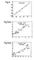
- Figure 4 is a correlation plot between the actual measured best-focus position and the calculated best-focus position based on Z9 and Z16 determined according to the present embodiment of the invention. Each square represents a different illumination setting of the apparatus. As can be seen, there is excellent correlation, with the maximum focus deviation from the fitted line always less than 10 nm.
- FIGs 5(a) and 5(b) These plot values of Z9 and Z16, respectively, as measured according to the present embodiment of the invention (FAMIS) against values of Z9 independently measured by the lens manufacturer using a technique referred to hereafter as SIF (Shearing InterFerometry).
- SIF is a through-the-lens (TTL) interferometric technique developed by the lens manufacturer.
- TTL through-the-lens
- the maximum deviation from the fit which can be related to the precision of the measurement technique, is approximately 1 nm Zernike. This is well below the tolerance with which the lens system is manufactured.
- the technique of the present invention has the advantage that it can be performed with the imaging system in situ in a lithographic projection apparatus.
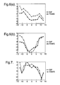
- Figure 6(a) and 6(b) show plots of Zernike coefficients Z9 and Z16 measured as a function of position in the x-direction, i.e. perpendicular to the scan direction in an apparatus used in scan mode as described above.
- the aberration data were measured on a step-and-scan system, but used in step mode.
- the aberration data are plotted for each x-position (along the slit), but averaged along the scan direction (y-direction), so the coefficients represent integrated values of Z9 and Z16.
- Each graph shows a plot of the Zernike coefficient measured according to the present FAMIS technique and as measured independently by the SIF technique.
- the graph in Figure 6(a) is a plot of the Z9 coefficient and the graph in Figure 6(b) is a plot of the Z16 coefficient. These graphs again show the good correlation between the two measurement techniques.
- the correlation plots of Figures 5(a) and 5(b) correspond to the data in the graphs of Figure 6(a) and 6(b) respectively, with regard to said x-position.
- Figure 7 shows results of measurements of the Z12 Zernike coefficient using the FAMIS technique of the present invention and using SIF.
- Z12 (which relates to the presence of astigmatism: see Figure 2) can be calculated using the present invention in the same way as Z9 or Z16, that is by computing the variation in astigmatism values (difference in best-focus position between x- and y- oriented lines) for a fixed amount of aberration due to, for example, a Z12 coefficient of 1 nm.
- the actual astigmatism values are measured at the same illumination settings, and a series of simultaneous equations formed and solved for Z12.
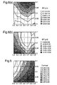
- Figures 8(a) and 8(b) are contour plots mapping the calculated best-focus position BF (from simulations) as a function of the NA and outer sigma value of the illumination setting, as a result of aberration represented by Zernike coefficients Z9 and Z16 (respectively in Figures 8(a) and 8(b)).
- the value of the respective Zernike coefficient was set at 10 nm.
- the technique according to the present invention can also be enhanced if it is desired to determine particular Zernike coefficients independently of each other.
- a contour line in the plot of Figure 8(a) substantially no variation in best-focus position will be caused by Z9 aberration, and therefore substantially all the best-focus position variation will be due to the Z16 (or other) Zernike coefficients.
- Z16 can be determined independently of Z9.
- Z9 can be determined independently of Z16 by taking measurements at illumination settings corresponding to contour lines in Figure 8(b).
- contrast should preferably be as high as possible. Contrast is mapped in Figure 9 as a function of the NA and outer sigma values of the illumination settings. As can be seen in Figure 9, contrast is maximized at high NA settings and low outer sigma settings.
- the parameter being measured can also be maximized by optimizing the structure being imaged, for example the type and size of the structure e.g. isolated lines and dense lines, isolated spaces, contact holes and so on, and by the choice of mask type, for example binary masks, attenuated masks and alternating phase-shift masks.
- the structure being imaged for example the type and size of the structure e.g. isolated lines and dense lines, isolated spaces, contact holes and so on, and by the choice of mask type, for example binary masks, attenuated masks and alternating phase-shift masks.
- the present invention can also be used to extract Zernike coefficients for odd aberrations.
- the present embodiment will be described in particular with reference to Zernike coefficient Z7, but could equally apply to other Zernike coefficients corresponding to aberrations with an odd value of m (see Figure 2). Odd aberrations result in a lateral shift of the image.
- Figure 10 is a table of computed lateral shift in the x-direction (also called x-shift, dX or ⁇ X) at eight different annular illumination settings; the settings of NA and sigma are given just as in Figure 3.
- the dX values are calculated on the basis of aberration due to a Zernike coefficient Z7 of 1 nm.
- the lateral shift in image position can be measured in an actual lithographic projection apparatus using a distortion-measuring technique hereinafter referred to as "DISTO" (described below); alternatively, one may directly measure the position of an aerial image, e.g. using a Transmission Image Sensor (TIS) (described above) or other technique mentioned in connection with the first embodiment.
- DISTO distortion-measuring technique
- TIS Transmission Image Sensor
- DISTO is a technique for finding the lateral positional errors of the image plane (x,y plane).
- a standard alignment mark consisting of horizontal and vertical equal lines/spaces (e.g. line width 8 pm for the imaged mark), is imaged on to a resist-coated wafer.
- the position of this imaged mark (latent or developed) can be measured by the alignment system of the lithographic apparatus.
- the deviation with respect to the expected position is the distortion. By distributing these marks over the whole image field, the complete image field distortion can be measured.
- DAMIS DISTO At Multiple Illumination Settings
- Z7 and Z14 can then be determined from the following relation, which gives the first-order correction to the measured shift in x-position resulting from X-coma due to non-zero Zernike coefficients Z7 and Z14:
- constants b and c in this case are now the Zernike coefficients Z7 and Z14, respectively, and can be obtained using the same matrix manipulation and multiple regression or least-square fitting as explained above in the first embodiment with reference to Z9 and Z16.
- term a is related to Z2, and is substantially constant.
- Figure 11 shows a plot of correlation between experimentally measured X-shift (plotted along the vertical axis, in nm) and the calculated shift caused by a Zernike coefficient Z7 of 1 nm (plotted along the horizontal axis, in nm).
- the plotted points and calculated shifts correspond to the illumination settings in the table of Figure 10.
- the gradient of the line of best-fit gives the extracted value of Z7 for this apparatus, which in this particular example gives Z7 approximately equal to 7 nm.
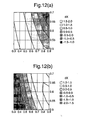
- Figures 12(a) and 12(b) show contour plots that map the shift dX in x-position in the illumination mode plane analogously to Figures 8(a) and 8(b).
- the accuracy of determination of Z7 or Z14, respectively can be improved, or variation due to one or other of Z7 and Z14 can be reduced or eliminated to separate its contribution to the aberration from that of the other coefficient, as explained above for Z9 and Z16 with respect to Figure 8.
- Figures 13(a) and 13(b) give further proof of the technique of the second embodiment of the invention. These Figures show plots ofZ7 (X-coma) and Z8 (Y-coma) as a function of x-position along the exposure slit. Values of the respective Zernike coefficients are plotted as obtained by the present invention and as independently measured using SIF. The correlation is again good.
- the sequence of operations consisted of calculating the expected shift in best-focus position or in x- or y-position using a simulation for different illumination settings, followed by measuring the actual shifts at those illumination settings, it may of course be more practical to take the measurements first at particular illumination settings and then to calculate the appropriate quantities using the simulation at the actual illumination settings at which measurements were taken.
- a sequence of test exposures is made sequentially, each with different NA and sigma settings, but with all other parameters of the exposures unchanged.
- the measurement using the first illumination setting can be repeated at the end, and possibly also once or more often between the intervening different illumination settings, of a given measurement sequence.
- lens aberration in terms of Zernike polynomials, but this is merely one of many possible sets of functions which can be used to describe wavefront aberrations, and the present invention can be used to measure aberrations in terms of parameters other than Zernike coefficients.
Landscapes
- Physics & Mathematics (AREA)
- General Physics & Mathematics (AREA)
- Exposure And Positioning Against Photoresist Photosensitive Materials (AREA)
- Exposure Of Semiconductors, Excluding Electron Or Ion Beam Exposure (AREA)
Claims (17)
- Procédé pour déterminer une aberration d'un système d'imagerie optique, comprenant :- un système de rayonnement (LA, Ex, IL) pour délivrer un faisceau de projection (PB) de rayonnement ;- une structure de support (MT) pour supporter des moyens de mise en forme (MA), les moyens de mise en forme (MA) servant à mettre en forme le faisceau de projection (PB) conformément à un motif voulu ;- une table de substrat (WT) pour maintenir un substrat (W) ; et- un système de projection (PL) pour projeter le faisceau mis en forme sur une partie cible du substrat (W) ; le procédé comprenant les étapes consistant à :caractérisé par l'étape consistant à :mettre en forme le faisceau de projection (PB) avec lesdits moyens de mise en forme (MA), etmesurer au moins un paramètre d'une image formée par le système de projection (PL), pour une pluralité de différents réglages dudit système de rayonnement (LA, Ex, IL) et/ou dudit système de projection (PL) ; etextraire un coefficient d'une expansion de l'aberration de front d'onde dudit système d'imagerie à partir des mesures dudit au moins un paramètre à ladite pluralité de réglages.
- Procédé selon revendication 1, dans lequel ladite pluralité de différents réglages comprend différents réglages d'ouverture numérique.
- Procédé selon la revendication 1 ou 2, dans lequel ladite pluralité de différents réglages comprend différents réglages de remplissage de pupille sur un plan de pupille dans le système d'imagerie.
- Procédé selon la revendication 1, 2 ou 3, dans lequel ladite pluralité de différents réglages comprend différents modes d'éclairage sélectionnés parmi le groupe comprenant un éclairage en forme de disque, annulaire, quadripolaire, dipolaire et multipolaire doux.
- Procédé selon l'une quelconque des revendications précédentes, dans lequel ladite pluralité de différents réglages comprend des réglages d'éclairage télécentrique et non-télécentrique, ou une pluralité de réglages d'éclairage non-télécentrique.
- Procédé selon l'une quelconque des revendications précédentes, dans lequel ledit au moins un paramètre est la position du meilleur foyer de ladite image.
- Procédé selon l'une quelconque des revendications précédentes, dans lequel ledit au moins un paramètre est la position latérale de ladite image.
- Procédé selon l'une quelconque des revendications précédentes, dans lequel ladite pluralité de différents réglages est sélectionnée de telle sorte que la variation du ou de chaque au moins un paramètre mesuré est sensiblement maximisée.
- Procédé selon l'une quelconque des revendications précédentes, dans lequel ladite pluralité de différents réglages est sélectionnée de telle sorte que la variation dudit au moins un paramètre mesuré résultant d'une aberration représentée par un ou plusieurs desdits coefficients est sensiblement égale à zéro, alors que la variation dudit au moins un paramètre en fonction d'un coefficient voulu n'est pas égale à zéro.
- Procédé selon l'une quelconque des revendications précédentes, comprenant en outre l'étape consistant à calculer une variation théorique, pour chaque réglage de ladite pluralité de différents réglages d'éclairage, du ou de chaque paramètre mesuré en fonction d'un petit changement dudit au moins un coefficient.
- Procédé selon l'une quelconque des revendications précédentes, dans lequel ledit au moins un coefficient est calculé par régression multiple ou par une méthode des moindres carrés d'un ensemble d'équations simultanées.
- Procédé selon l'une quelconque des revendications précédentes, dans lequel ledit au moins un coefficient est un coefficient de Zernike.
- Appareil de projection lithographique pour projeter un faisceau de rayonnement mis en forme sur un substrat muni d'une couche sensible au rayonnement, l'appareil comprenant :- un système de rayonnement (LA, Ex, IL) pour délivrer un faisceau de projection (PB) de rayonnement ;- une structure de support (MT) pour supporter des moyens de mise en forme (MA), les moyens de mise en forme (MA) servant à mettre en forme le faisceau de projection (PB) conformément à un motif voulu ;- une table de substrat (WT) pour maintenir un substrat (W) ;- un système de projection (PL) pour projeter le faisceau mis en forme (PB) sur une partie cible du substrat (W) ;- des moyens de réglage d'éclairage pour fournir une pluralité de différents réglages d'éclairage dudit système de rayonnement (LA, Ex, IL) et/ou dudit système de projection (PL) ;- des moyens de mesure pour mesurer au moins un paramètre d'une image projetée formée par le système de projection ;- des moyens de contrôle pour sélectionner une pluralité de différents réglages d'éclairage auxquels lesdits moyens de mesure prennent des mesures ; etcaractérisé en ce qu'il comprend en outre :- des moyens de calcul agencés pour extraire un coefficient d'une expansion de l'aberration de front d'onde dudit système de projection et/ou de rayonnement à partir des mesures dudit au moins un paramètre mesuré par lesdits moyens de mesure à ladite pluralité de différents réglages d'éclairage.
- Appareil selon la revendication 13, dans lequel la structure de support (MT) comprend une table de masque pour maintenir un masque.
- Appareil selon la revendication 13, dans lequel le système de rayonnement (LA, Ex, IL) comprend une source de rayonnement (LA).
- Procédé de fabrication d'un dispositif utilisant un appareil de projection lithographique, comprenant les étapes consistant à :(a) fournir un substrat (W) qui est au moins partiellement recouvert d'une couche de matériau sensible au rayonnement ;(b) fournir un faisceau de projection (PB) de rayonnement utilisant un système de rayonnement (LA, Ex, IL) ;(c) utiliser des moyens de mise en forme (MA) pour doter le faisceau de projection (PB) d'un motif dans sa section transversale ;(d) utiliser un système de projection (PL) pour projeter le faisceau de rayonnement mis en forme sur une partie cible de la couche de matériau sensible au rayonnement,et comprenant en outre l'étape consistant à :mesurer, avant l'étape (d), au moins un paramètre d'une image formée par le système de projection (PL), pour une pluralité de différents réglages dudit système de rayonnement (LA, Ex, IL) et/ou dudit système de projection (PL) ;caractérisé par les étapes consistant à :extraire un coefficient d'une expansion de l'aberration de front d'onde dudit système de projection et/ou de rayonnement à partir des mesures dudit au moins un paramètre à ladite pluralité de réglages ; etcorriger ladite aberration sur la base dudit coefficient extrait, pour réduire l'aberration d'une image projetée par ledit système de projection.
- Procédé selon la revendication 16, dans lequel ladite étape de correction comprend la correction de changements de position latérale et/ou de meilleur foyer de ladite image lors d'un changement entre différents réglages d'éclairage.
Priority Applications (1)
| Application Number | Priority Date | Filing Date | Title |
|---|---|---|---|
| EP01301571A EP1128217B1 (fr) | 2000-02-23 | 2001-02-21 | Méthode de mesure des aberrations dans un système optique de formation d'image |
Applications Claiming Priority (3)
| Application Number | Priority Date | Filing Date | Title |
|---|---|---|---|
| EP00301420 | 2000-02-23 | ||
| EP00301420 | 2000-02-23 | ||
| EP01301571A EP1128217B1 (fr) | 2000-02-23 | 2001-02-21 | Méthode de mesure des aberrations dans un système optique de formation d'image |
Publications (3)
| Publication Number | Publication Date |
|---|---|
| EP1128217A2 EP1128217A2 (fr) | 2001-08-29 |
| EP1128217A3 EP1128217A3 (fr) | 2004-12-29 |
| EP1128217B1 true EP1128217B1 (fr) | 2007-08-29 |
Family
ID=26073017
Family Applications (1)
| Application Number | Title | Priority Date | Filing Date |
|---|---|---|---|
| EP01301571A Expired - Lifetime EP1128217B1 (fr) | 2000-02-23 | 2001-02-21 | Méthode de mesure des aberrations dans un système optique de formation d'image |
Country Status (1)
| Country | Link |
|---|---|
| EP (1) | EP1128217B1 (fr) |
Families Citing this family (13)
| Publication number | Priority date | Publication date | Assignee | Title |
|---|---|---|---|---|
| JPWO2002052620A1 (ja) | 2000-12-22 | 2004-04-30 | 株式会社ニコン | 波面収差測定装置、波面収差測定方法、露光装置及びマイクロデバイスの製造方法 |
| WO2002054036A1 (fr) | 2000-12-28 | 2002-07-11 | Nikon Corporation | Procede de mesure et d'ajustement de caracteristiques d'imagerie, procede et systeme d'exposition, programme et support d'enregistrement et procede de production de dispositif |
| TWI220998B (en) * | 2001-02-13 | 2004-09-11 | Nikon Corp | Exposure method, exposure apparatus and manufacture method of the same |
| US6956659B2 (en) | 2001-05-22 | 2005-10-18 | Nikon Precision Inc. | Measurement of critical dimensions of etched features |
| DE10146499B4 (de) * | 2001-09-21 | 2006-11-09 | Carl Zeiss Smt Ag | Verfahren zur Optimierung der Abbildungseigenschaften von mindestens zwei optischen Elementen sowie Verfahren zur Optimierung der Abbildungseigenschaften von mindestens drei optischen Elementen |
| KR100927560B1 (ko) | 2002-01-29 | 2009-11-23 | 가부시키가이샤 니콘 | 이미지 형성 상태 조정 시스템, 노광 방법 및 노광 장치, 그리고 프로그램 및 정보 기록 매체 |
| JP2003257812A (ja) | 2002-02-27 | 2003-09-12 | Nikon Corp | 結像光学系の評価方法、結像光学系の調整方法、露光装置および露光方法 |
| JP4352458B2 (ja) | 2002-03-01 | 2009-10-28 | 株式会社ニコン | 投影光学系の調整方法、予測方法、評価方法、調整方法、露光方法及び露光装置、露光装置の製造方法、プログラム並びにデバイス製造方法 |
| US6974653B2 (en) | 2002-04-19 | 2005-12-13 | Nikon Precision Inc. | Methods for critical dimension and focus mapping using critical dimension test marks |
| US7403264B2 (en) | 2004-07-08 | 2008-07-22 | Asml Netherlands B.V. | Lithographic projection apparatus and a device manufacturing method using such lithographic projection apparatus |
| US7262831B2 (en) | 2004-12-01 | 2007-08-28 | Asml Netherlands B.V. | Lithographic projection apparatus and device manufacturing method using such lithographic projection apparatus |
| US7605914B2 (en) | 2005-09-29 | 2009-10-20 | Carl Zeiss Smt Ag | Optical system and method for improving imaging properties thereof |
| EP1795967B1 (fr) * | 2005-12-09 | 2010-05-05 | Imec | Procédés et dispositifs pour lithographie |
Family Cites Families (2)
| Publication number | Priority date | Publication date | Assignee | Title |
|---|---|---|---|---|
| US5754299A (en) * | 1995-01-13 | 1998-05-19 | Nikon Corporation | Inspection apparatus and method for optical system, exposure apparatus provided with the inspection apparatus, and alignment apparatus and optical system thereof applicable to the exposure apparatus |
| JP3256678B2 (ja) * | 1998-02-19 | 2002-02-12 | 株式会社東芝 | レンズの収差測定方法 |
-
2001
- 2001-02-21 EP EP01301571A patent/EP1128217B1/fr not_active Expired - Lifetime
Non-Patent Citations (1)
| Title |
|---|
| None * |
Also Published As
| Publication number | Publication date |
|---|---|
| EP1128217A2 (fr) | 2001-08-29 |
| EP1128217A3 (fr) | 2004-12-29 |
Similar Documents
| Publication | Publication Date | Title |
|---|---|---|
| US6646729B2 (en) | Method of measuring aberration in an optical imaging system | |
| EP1626310B1 (fr) | Appareil lithographique et méthode pour la fabrication d'un dispositif | |
| US6563564B2 (en) | Method of operating an optical imaging system, lithographic projection apparatus, device manufacturing method, and device manufactured thereby | |
| KR100562190B1 (ko) | 리소그래피장치의 투영시스템의 수차를 측정하는 방법,디바이스제조방법, 및 그 제조된 디바이스 | |
| KR100585211B1 (ko) | 리소그래피장치, 디바이스제조방법 및 그에 따라 제조된디바이스 | |
| US7262831B2 (en) | Lithographic projection apparatus and device manufacturing method using such lithographic projection apparatus | |
| TWI266148B (en) | Lithographic apparatus and device manufacturing method | |
| TWI285299B (en) | Lithographic manufacturing process, lithographic projection apparatus, and device manufactured thereby | |
| US20050210438A1 (en) | Modification of an image of a pattern during an imaging process | |
| US20090042139A1 (en) | Exposure method and electronic device manufacturing method | |
| EP1128217B1 (fr) | Méthode de mesure des aberrations dans un système optique de formation d'image | |
| EP1251402B1 (fr) | Appareil lithographique et méthode de fabrication d'un dispositif | |
| US7558643B2 (en) | Lithographic apparatus, method of determining a model parameter, device manufacturing method, and device manufactured thereby | |
| US6897947B1 (en) | Method of measuring aberration in an optical imaging system | |
| US6987555B2 (en) | Lithographic apparatus, device manufacturing method, and device manufactured thereby | |
| US7253077B2 (en) | Substrate, method of preparing a substrate, method of measurement, lithographic apparatus, device manufacturing method and device manufactured thereby, and machine-readable storage medium | |
| EP1164436A2 (fr) | Opération d'un appareil de projection lithographique | |
| EP1286223B1 (fr) | Méthode de mesure de l'aberration d'un système de projection lithographique | |
| CN101652719A (zh) | 曝光方法及电子器件制造方法 | |
| WO2025228613A1 (fr) | Procédé et système de mesure pour déterminer des données relatives à des aberrations provoquées par un système de projection |
Legal Events
| Date | Code | Title | Description |
|---|---|---|---|
| PUAI | Public reference made under article 153(3) epc to a published international application that has entered the european phase |
Free format text: ORIGINAL CODE: 0009012 |
|
| AK | Designated contracting states |
Kind code of ref document: A2 Designated state(s): AT BE CH CY DE DK ES FI FR GB GR IE IT LI LU MC NL PT SE TR |
|
| AX | Request for extension of the european patent |
Free format text: AL;LT;LV;MK;RO;SI |
|
| RAP1 | Party data changed (applicant data changed or rights of an application transferred) |
Owner name: ASML NETHERLANDS B.V. |
|
| RAP1 | Party data changed (applicant data changed or rights of an application transferred) |
Owner name: ASML NETHERLANDS B.V. |
|
| PUAL | Search report despatched |
Free format text: ORIGINAL CODE: 0009013 |
|
| AK | Designated contracting states |
Kind code of ref document: A3 Designated state(s): AT BE CH CY DE DK ES FI FR GB GR IE IT LI LU MC NL PT SE TR |
|
| AX | Request for extension of the european patent |
Extension state: AL LT LV MK RO SI |
|
| 17P | Request for examination filed |
Effective date: 20050426 |
|
| AKX | Designation fees paid |
Designated state(s): DE FR GB IT NL |
|
| GRAP | Despatch of communication of intention to grant a patent |
Free format text: ORIGINAL CODE: EPIDOSNIGR1 |
|
| GRAS | Grant fee paid |
Free format text: ORIGINAL CODE: EPIDOSNIGR3 |
|
| GRAA | (expected) grant |
Free format text: ORIGINAL CODE: 0009210 |
|
| AK | Designated contracting states |
Kind code of ref document: B1 Designated state(s): DE FR GB IT NL |
|
| REG | Reference to a national code |
Ref country code: GB Ref legal event code: FG4D |
|
| REF | Corresponds to: |
Ref document number: 60130160 Country of ref document: DE Date of ref document: 20071011 Kind code of ref document: P |
|
| ET | Fr: translation filed | ||
| PGFP | Annual fee paid to national office [announced via postgrant information from national office to epo] |
Ref country code: NL Payment date: 20080214 Year of fee payment: 8 Ref country code: IT Payment date: 20080223 Year of fee payment: 8 Ref country code: GB Payment date: 20080220 Year of fee payment: 8 Ref country code: DE Payment date: 20080219 Year of fee payment: 8 |
|
| PLBE | No opposition filed within time limit |
Free format text: ORIGINAL CODE: 0009261 |
|
| STAA | Information on the status of an ep patent application or granted ep patent |
Free format text: STATUS: NO OPPOSITION FILED WITHIN TIME LIMIT |
|
| PGFP | Annual fee paid to national office [announced via postgrant information from national office to epo] |
Ref country code: FR Payment date: 20080214 Year of fee payment: 8 |
|
| 26N | No opposition filed |
Effective date: 20080530 |
|
| GBPC | Gb: european patent ceased through non-payment of renewal fee |
Effective date: 20090221 |
|
| NLV4 | Nl: lapsed or anulled due to non-payment of the annual fee |
Effective date: 20090901 |
|
| REG | Reference to a national code |
Ref country code: FR Ref legal event code: ST Effective date: 20091030 |
|
| PG25 | Lapsed in a contracting state [announced via postgrant information from national office to epo] |
Ref country code: NL Free format text: LAPSE BECAUSE OF NON-PAYMENT OF DUE FEES Effective date: 20090901 |
|
| PG25 | Lapsed in a contracting state [announced via postgrant information from national office to epo] |
Ref country code: DE Free format text: LAPSE BECAUSE OF NON-PAYMENT OF DUE FEES Effective date: 20090901 |
|
| PG25 | Lapsed in a contracting state [announced via postgrant information from national office to epo] |
Ref country code: GB Free format text: LAPSE BECAUSE OF NON-PAYMENT OF DUE FEES Effective date: 20090221 Ref country code: FR Free format text: LAPSE BECAUSE OF NON-PAYMENT OF DUE FEES Effective date: 20090302 |
|
| PG25 | Lapsed in a contracting state [announced via postgrant information from national office to epo] |
Ref country code: IT Free format text: LAPSE BECAUSE OF NON-PAYMENT OF DUE FEES Effective date: 20090221 |