EP1164436A2 - Opération d'un appareil de projection lithographique - Google Patents
Opération d'un appareil de projection lithographique Download PDFInfo
- Publication number
- EP1164436A2 EP1164436A2 EP01305099A EP01305099A EP1164436A2 EP 1164436 A2 EP1164436 A2 EP 1164436A2 EP 01305099 A EP01305099 A EP 01305099A EP 01305099 A EP01305099 A EP 01305099A EP 1164436 A2 EP1164436 A2 EP 1164436A2
- Authority
- EP
- European Patent Office
- Prior art keywords
- radiation
- parameters
- projection
- calibration
- aberration
- Prior art date
- Legal status (The legal status is an assumption and is not a legal conclusion. Google has not performed a legal analysis and makes no representation as to the accuracy of the status listed.)
- Ceased
Links
- 230000004075 alteration Effects 0.000 claims abstract description 82
- 230000000694 effects Effects 0.000 claims abstract description 66
- 238000000034 method Methods 0.000 claims abstract description 55
- 238000010438 heat treatment Methods 0.000 claims abstract description 48
- 230000008859 change Effects 0.000 claims abstract description 23
- 230000005855 radiation Effects 0.000 claims description 65
- 239000000758 substrate Substances 0.000 claims description 58
- 238000005286 illumination Methods 0.000 claims description 42
- 230000006870 function Effects 0.000 claims description 23
- 238000002310 reflectometry Methods 0.000 claims description 22
- 230000003287 optical effect Effects 0.000 claims description 21
- 238000000059 patterning Methods 0.000 claims description 19
- 238000012937 correction Methods 0.000 claims description 12
- 238000004519 manufacturing process Methods 0.000 claims description 11
- 239000000463 material Substances 0.000 claims description 11
- 201000009310 astigmatism Diseases 0.000 claims description 8
- 230000015654 memory Effects 0.000 claims description 6
- 231100000812 repeated exposure Toxicity 0.000 claims description 4
- 235000012431 wafers Nutrition 0.000 description 49
- 238000005259 measurement Methods 0.000 description 26
- 239000010410 layer Substances 0.000 description 21
- 229920002120 photoresistant polymer Polymers 0.000 description 14
- 230000005540 biological transmission Effects 0.000 description 9
- 238000003384 imaging method Methods 0.000 description 7
- 238000001816 cooling Methods 0.000 description 6
- 238000009826 distribution Methods 0.000 description 6
- 239000011159 matrix material Substances 0.000 description 6
- 230000008569 process Effects 0.000 description 5
- 238000012545 processing Methods 0.000 description 5
- 210000001747 pupil Anatomy 0.000 description 5
- 238000012360 testing method Methods 0.000 description 5
- 230000001419 dependent effect Effects 0.000 description 4
- 206010010071 Coma Diseases 0.000 description 3
- XUIMIQQOPSSXEZ-UHFFFAOYSA-N Silicon Chemical compound [Si] XUIMIQQOPSSXEZ-UHFFFAOYSA-N 0.000 description 3
- 230000000873 masking effect Effects 0.000 description 3
- 230000009467 reduction Effects 0.000 description 3
- 229910052710 silicon Inorganic materials 0.000 description 3
- 239000010703 silicon Substances 0.000 description 3
- 230000006399 behavior Effects 0.000 description 2
- 230000008901 benefit Effects 0.000 description 2
- 239000011248 coating agent Substances 0.000 description 2
- 238000000576 coating method Methods 0.000 description 2
- 238000013461 design Methods 0.000 description 2
- 230000001066 destructive effect Effects 0.000 description 2
- 238000000691 measurement method Methods 0.000 description 2
- QSHDDOUJBYECFT-UHFFFAOYSA-N mercury Chemical compound [Hg] QSHDDOUJBYECFT-UHFFFAOYSA-N 0.000 description 2
- 229910052753 mercury Inorganic materials 0.000 description 2
- 230000003278 mimic effect Effects 0.000 description 2
- 230000010363 phase shift Effects 0.000 description 2
- 230000011218 segmentation Effects 0.000 description 2
- 230000035945 sensitivity Effects 0.000 description 2
- 101000720958 Homo sapiens Protein artemis Proteins 0.000 description 1
- 229910001374 Invar Inorganic materials 0.000 description 1
- 102100025918 Protein artemis Human genes 0.000 description 1
- 238000010521 absorption reaction Methods 0.000 description 1
- 230000032683 aging Effects 0.000 description 1
- 239000006117 anti-reflective coating Substances 0.000 description 1
- 238000003491 array Methods 0.000 description 1
- 230000002238 attenuated effect Effects 0.000 description 1
- 238000004061 bleaching Methods 0.000 description 1
- WUKWITHWXAAZEY-UHFFFAOYSA-L calcium difluoride Chemical compound [F-].[F-].[Ca+2] WUKWITHWXAAZEY-UHFFFAOYSA-L 0.000 description 1
- 229910001634 calcium fluoride Inorganic materials 0.000 description 1
- 238000004364 calculation method Methods 0.000 description 1
- 238000005056 compaction Methods 0.000 description 1
- 230000003750 conditioning effect Effects 0.000 description 1
- 238000002939 conjugate gradient method Methods 0.000 description 1
- 238000010276 construction Methods 0.000 description 1
- 238000001514 detection method Methods 0.000 description 1
- 238000011161 development Methods 0.000 description 1
- 230000018109 developmental process Effects 0.000 description 1
- 238000006073 displacement reaction Methods 0.000 description 1
- 230000005670 electromagnetic radiation Effects 0.000 description 1
- 238000010894 electron beam technology Methods 0.000 description 1
- 238000005530 etching Methods 0.000 description 1
- 238000013213 extrapolation Methods 0.000 description 1
- 230000004907 flux Effects 0.000 description 1
- 230000017525 heat dissipation Effects 0.000 description 1
- CPBQJMYROZQQJC-UHFFFAOYSA-N helium neon Chemical compound [He].[Ne] CPBQJMYROZQQJC-UHFFFAOYSA-N 0.000 description 1
- 238000007689 inspection Methods 0.000 description 1
- 238000005468 ion implantation Methods 0.000 description 1
- 239000002346 layers by function Substances 0.000 description 1
- 239000004973 liquid crystal related substance Substances 0.000 description 1
- 238000001459 lithography Methods 0.000 description 1
- 230000005381 magnetic domain Effects 0.000 description 1
- 238000001465 metallisation Methods 0.000 description 1
- 238000012986 modification Methods 0.000 description 1
- 230000004048 modification Effects 0.000 description 1
- 230000003647 oxidation Effects 0.000 description 1
- 238000007254 oxidation reaction Methods 0.000 description 1
- 230000001575 pathological effect Effects 0.000 description 1
- 238000005498 polishing Methods 0.000 description 1
- 230000037452 priming Effects 0.000 description 1
- 239000010453 quartz Substances 0.000 description 1
- 238000005070 sampling Methods 0.000 description 1
- 239000004065 semiconductor Substances 0.000 description 1
- 238000007493 shaping process Methods 0.000 description 1
- 238000009416 shuttering Methods 0.000 description 1
- VYPSYNLAJGMNEJ-UHFFFAOYSA-N silicon dioxide Inorganic materials O=[Si]=O VYPSYNLAJGMNEJ-UHFFFAOYSA-N 0.000 description 1
- 238000003860 storage Methods 0.000 description 1
- 239000010409 thin film Substances 0.000 description 1
Images

Classifications
-
- G—PHYSICS
- G03—PHOTOGRAPHY; CINEMATOGRAPHY; ANALOGOUS TECHNIQUES USING WAVES OTHER THAN OPTICAL WAVES; ELECTROGRAPHY; HOLOGRAPHY
- G03F—PHOTOMECHANICAL PRODUCTION OF TEXTURED OR PATTERNED SURFACES, e.g. FOR PRINTING, FOR PROCESSING OF SEMICONDUCTOR DEVICES; MATERIALS THEREFOR; ORIGINALS THEREFOR; APPARATUS SPECIALLY ADAPTED THEREFOR
- G03F7/00—Photomechanical, e.g. photolithographic, production of textured or patterned surfaces, e.g. printing surfaces; Materials therefor, e.g. comprising photoresists; Apparatus specially adapted therefor
- G03F7/70—Microphotolithographic exposure; Apparatus therefor
- G03F7/70483—Information management; Active and passive control; Testing; Wafer monitoring, e.g. pattern monitoring
- G03F7/70591—Testing optical components
- G03F7/706—Aberration measurement
-
- G—PHYSICS
- G03—PHOTOGRAPHY; CINEMATOGRAPHY; ANALOGOUS TECHNIQUES USING WAVES OTHER THAN OPTICAL WAVES; ELECTROGRAPHY; HOLOGRAPHY
- G03F—PHOTOMECHANICAL PRODUCTION OF TEXTURED OR PATTERNED SURFACES, e.g. FOR PRINTING, FOR PROCESSING OF SEMICONDUCTOR DEVICES; MATERIALS THEREFOR; ORIGINALS THEREFOR; APPARATUS SPECIALLY ADAPTED THEREFOR
- G03F7/00—Photomechanical, e.g. photolithographic, production of textured or patterned surfaces, e.g. printing surfaces; Materials therefor, e.g. comprising photoresists; Apparatus specially adapted therefor
- G03F7/70—Microphotolithographic exposure; Apparatus therefor
- G03F7/70216—Mask projection systems
-
- G—PHYSICS
- G03—PHOTOGRAPHY; CINEMATOGRAPHY; ANALOGOUS TECHNIQUES USING WAVES OTHER THAN OPTICAL WAVES; ELECTROGRAPHY; HOLOGRAPHY
- G03F—PHOTOMECHANICAL PRODUCTION OF TEXTURED OR PATTERNED SURFACES, e.g. FOR PRINTING, FOR PROCESSING OF SEMICONDUCTOR DEVICES; MATERIALS THEREFOR; ORIGINALS THEREFOR; APPARATUS SPECIALLY ADAPTED THEREFOR
- G03F7/00—Photomechanical, e.g. photolithographic, production of textured or patterned surfaces, e.g. printing surfaces; Materials therefor, e.g. comprising photoresists; Apparatus specially adapted therefor
- G03F7/70—Microphotolithographic exposure; Apparatus therefor
- G03F7/708—Construction of apparatus, e.g. environment aspects, hygiene aspects or materials
- G03F7/70858—Environment aspects, e.g. pressure of beam-path gas, temperature
- G03F7/70883—Environment aspects, e.g. pressure of beam-path gas, temperature of optical system
- G03F7/70891—Temperature
Definitions
- the present invention relates to a method of operating a lithographic projection apparatus comprising:
- patterning means as here employed should be broadly interpreted as referring to means that can be used to endow an incoming radiation beam with a patterned cross-section, corresponding to a pattern that is to be created in a target portion of the substrate; the term “light valve” can also be used in this context.
- the said pattern will correspond to a particular functional layer in a device being created in the target portion, such as an integrated circuit or other device (see below). Examples of such patterning means include:
- Lithographic projection apparatus can be used, for example, in the manufacture of integrated circuits (ICs).
- the patterning means may generate a circuit pattern corresponding to an individual layer of the IC, and this pattern can be imaged onto a target portion (e.g. comprising one or more dies) on a substrate (silicon wafer) that has been coated with a layer of radiation-sensitive material (resist).
- a target portion e.g. comprising one or more dies
- a substrate silicon wafer
- a layer of radiation-sensitive material resist
- a single wafer will contain a whole network of adjacent target portions that are successively irradiated via the projection system, one at a time.
- employing patterning by a mask on a mask table a distinction can be made between two different types of machine.
- each target portion is irradiated by exposing the entire mask pattern onto the target portion in one go; such an apparatus is commonly referred to as a wafer stepper.
- each target portion is irradiated by progressively scanning the mask pattern under the projection beam in a given reference direction (the "scanning" direction) while synchronously scanning the substrate table parallel or anti-parallel to this direction; since, in general, the projection system will have a magnification factor M (generally ⁇ 1), the speed V at which the substrate table is scanned will be a factor M times that at which the mask table is scanned.
- M magnification factor
- a pattern (e.g. in a mask) is imaged onto a substrate that is at least partially covered by a layer of radiation-sensitive material (resist).
- the substrate Prior to this imaging step, the substrate may undergo various procedures, such as priming, resist coating and a soft bake. After exposure, the substrate may be subjected to other procedures, such as a post-exposure bake (PEB), development, a hard bake and measurement/inspection of the imaged features.
- PEB post-exposure bake
- This array of procedures is used as a basis to pattern an individual layer of a device, e.g. an IC.
- Such a patterned layer may then undergo various processes such as etching, ion-implantation (doping), metallization, oxidation, chemo-mechanical polishing, etc., all intended to finish off an individual layer.
- alignment accuracy An important aspect of the performance of a lithographic projection apparatus is the so-called alignment accuracy.
- a small reference mark is provided at one or more positions on the wafer, thus defining the origin of a co-ordinate system on the wafer; using optical and electronic means (referred to hereinafter as "alignment system"), this mark can then be relocated each time a new layer has to be juxtaposed on an existing layer, and can be used as an alignment reference.
- the projection system may hereinafter be referred to as the "lens"; however, this term should be broadly interpreted as encompassing various types of projection system, including refractive optics, reflective optics, and catadioptric systems, for example.
- the radiation system may also include components operating according to any of these design types for directing, shaping or controlling the projection beam of radiation, and such components may also be referred to below, collectively or singularly, as a "lens”.
- the lithographic apparatus may be of a type having two or more substrate tables (and/or two or more mask tables). In such "multiple stage” devices the additional tables may be used in parallel, or preparatory steps may be carried out on one or more tables while one or more other tables are being used for exposures. Twin stage lithographic apparatus are described, for example, in US 5,969,441 and WO 98/40791, incorporated herein by reference.
- the phenomenon of lens heating can occur in the projection system of a lithographic projection apparatus.
- the projection lens becomes slightly heated by the projection beam radiation during exposures.
- refractive index changes occur, and a certain expansion of lens elements occurs, causing subtle changes in the geometric form of those elements, with an attendant change in their optical properties.
- This can result in the occurrence of new lens aberrations, or a change in existing aberrations. Because the occurrence or worsening of these aberrations depends on such matters as the particular lens geometry, lens material, projection wavelength, light source power, target portion size, and so on, the phenomenon is intrinsically unpredictable.
- Lens heating has always occurred to some extent in lithographic projection apparatus.
- shorter wavelength radiation such as deep ultraviolet (DUV)
- 193 nm and 157 nm radiation has been used, as well as high-power radiation sources, such as 3-6 kW
- Mercury-arc lamps and excimer lasers with a power of 10 to 20 W which together with the reduction in feature size have made lens heating a more serious problem.
- the problem is generally worse in scanners than in steppers because, in a stepper, substantially the whole (circular) cross-section of each lens element is irradiated, whereas, in a scanner, generally only a slit-shaped portion of the lens elements is irradiated; consequently, the effect in a scanner is far more differential than in a stepper, thereby resulting in the occurrence of new lens aberrations.
- the present invention provides a method of operating a lithographic projection apparatus as specified in the opening paragraph, the method characterized by comprising the steps of:
- the calibration step may comprise a coarse calibration followed by at least one fine calibration, where the coarse calibration yields a first estimate of at least a subset of the parameters. Said first estimate can be used as an input for the subsequent fine calibration.
- first estimates of parameters may, for example, be available from design data or empirical evidence. In this latter case the calibration may comprise a single (fine) calibration step.
- a (fine) calibration is successively performed at a plurality of different illumination settings and/or with a plurality of different patterns as provided by patterning means and/or with a plurality of different substrates provided on said substrate table, wherein a set of parameters is obtained for each calibration, and the sets of parameters from the calibrations are stored in a database.
- Said plurality of different illumination settings may comprise different numerical aperture settings and/or sigma settings (defined below), illumination modes or telecentricity modes; furthermore, one may use various types and sizes of test structures on one or more test masks to create different diffraction effects in the projection system. All such variation should be interpreted as falling within the meaning of the phrase "different illumination settings” of the radiation system, as used in this text.
- the term "sigma ( ⁇ ) setting” refers to the outer and/or inner radial extent (commonly referred to as ⁇ -outer and ⁇ -inner, respectively) of the intensity distribution of the projection beam in a pupil plane of the radiation system, normalized with respect to the maximum radius of the pupil.
- illumination mode denotes the spatial distribution of the radiation at the pupil, which may, for example, be disc-shaped, annular (which would be characterized by inner and outer sigma settings), quadrupolar, dipolar, or soft-multipolar (including some radiation flux in between and/or around the poles), for example. More information on illumination modes can be gleaned, for example, from European Patent Application No. 00311007.9, incorporated herein by reference.
- telecentricity modes encompasses configuring the radiation system and/or projection system telecentrically and/or with varying degrees of non-telecentricity, for example by the use of prisms on top of a reticle to tilt the illumination profile. These different illumination settings can be selected conveniently in a lithographic projection apparatus.
- said calculating step comprises interpolating or extrapolating at least one of said parameters based on parameters obtained for the projection apparatus under different conditions.
- said aberration effect comprises at least one of focus drift, field curvature, magnification drift, third-order distortion, spherical aberration, comatic aberration, on-axis astigmatism, asymmetric magnification and combinations thereof.
- said adjusting step comprises adjusting at least one of: the position of the support structure along the optical axis of the projection system, the rotational orientation of the support structure, the position of the substrate table along said optical axis, the rotational orientation of the substrate table, the position along said optical axis of one or more moveable lens elements comprised in said projection system, the degree of decentering with respect to said optical axis of one or more moveable lens elements comprised in said projection system, the central wavelength of the projection beam, and saddle-like deformation of one or more lens elements comprised in said projection system using edge actuators.
- the present invention also provides a lithographic projection apparatus for imaging a pattern as provided by patterning means onto a substrate provided with a radiation-sensitive layer, the apparatus comprising:
- a device manufacturing method comprising the steps of:
- the terms "radiation” and “beam” are used to encompass all types of electromagnetic radiation, including ultraviolet radiation (e.g. with a wavelength of 365, 248, 193, 157 or 126 nm) and EUV (extreme ultra-violet radiation, e.g. having a wavelength in the range 5-20 nm).
- ultraviolet radiation e.g. with a wavelength of 365, 248, 193, 157 or 126 nm
- EUV extreme ultra-violet radiation
- Figure 1 schematically depicts a lithographic projection apparatus according to a particular embodiment of the invention.
- the apparatus comprises:
- the source LA e.g. a Mercury arc lamp, a DUV excimer laser, a laser-produced plasma source, a discharge source, or an undulator or wiggler provided around the path of an electron beam in a storage ring or synchrotron
- the source LA produces a beam of radiation.
- This beam is fed into an illumination system (illuminator) IL, either directly or after having traversed conditioning means, such as a beam expander Ex, for example.
- the illuminator IL may comprise adjusting means AM for setting ⁇ -outer and ⁇ -inner, respectively.
- it will generally comprise various other components, such as an integrator IN and a condenser CO.
- the beam PB impinging on the mask MA has a desired uniformity and intensity distribution in its cross-section.
- the source LA may be within the housing of the lithographic projection apparatus (as is often the case when the source LA is a mercury lamp, for example), but that it may also be remote from the lithographic projection apparatus, the radiation beam which it produces being led into the apparatus (e.g. with the aid of suitable directing mirrors); this latter scenario is often the case when the source LA is an excimer laser.
- the current invention and Claims encompass both of these scenarios.
- the beam PB subsequently intercepts the mask MA, which is held on a mask table MT. Having traversed the mask MA, the beam PB passes through the lens PL, which focuses the beam PB onto a target portion C of the substrate W. With the aid of the second positioning means (and interferometric measuring means IF), the substrate table WT can be moved accurately, e.g. so as to position different target portions C in the path of the beam PB. Similarly, the first positioning means can be used to accurately position the mask MA with respect to the path of the beam PB, e.g. after mechanical retrieval of the mask MA from a mask library, or during a scan.
- the mask table MT may just be connected to a short stroke actuator, or may be fixed.
- the depicted apparatus can be used in two different modes:
- the projection beam radiation PB passes though the projection lens system PL, part of it is absorbed in lens elements and coating materials. This partial absorption causes global and local temperature and refractive index changes in the lens elements. This results in changes in the optical performance of the lens, which can be characterized as lens aberration.
- the overall aberration can be decomposed into a number of different types of aberration, such as spherical aberration, astigmatism and so on.
- the overall aberration is the sum of these different aberrations, each with a particular magnitude given by a coefficient. Aberration results in a deformation in the wave front and different types of aberration represent different functions by which the wave front is deformed.
- Other aberrations such as magnification drift, third-order distortion, asymmetric magnification, coma, and aberrations with an odd value of m, result in a lateral shift in the image position in the horizontal plane (the x , y -plane).
- the best-focus (BF) position i.e. z-position of the image
- the best-focus position is the z-position with maximum contrast, e.g. defined by the maximum of a sixth-order polynomial fit to the contrast-versus-position curve as the position is moved from defocus, through focus and on to defocus.
- the best-focus can be determined experimentally using known techniques, such as the technique known as "FOCAL" (described below); alternatively, one may directly measure the aerial image, e.g. using a Transmission Image Sensor (TIS) (described below), or an overlay microscope or commercial focus monitor.
- TIS Transmission Image Sensor
- FOCAL is an acronym for FO cus C alibration by using AL ignment. It is a best-focus measurement technique for completely determining information about the focal plane using the alignment system of the lithographic apparatus.
- a special, asymmetrically segmented alignment mark is imaged through focus on to a resist coated wafer. The position of this imaged mark (latent or developed) can be measured by the said alignment system. Due to the asymmetric segmentation, the position measured by the alignment system will depend on the defocus used during exposure, thus allowing determination of the best-focus position. By distributing these marks over the whole image field and using different orientation for the segmentation, the complete focal plane for several structure orientations can be measured. This technique is described in more detail in US 5,674,650 which is incorporated herein by reference.
- One or more transmission image sensor(s) can be used to determine the lateral position and best focus position (i.e. horizontal and vertical position) of the projected image from the mask under the projection lens.
- a transmission image sensor (TIS) is inset into a physical reference surface associated with the substrate table (WT).
- two sensors are mounted on fiducial plates mounted to the substrate-bearing surface of the substrate table (WT), at diagonally opposite positions outside the area covered by the wafer W.
- Each fiducial plate is made of a highly stable material with a very low coefficient of thermal expansion, e.g. Invar, and has a flat reflective upper surface which may carry markers used with another fiducial in alignment processes.
- the TIS is used to determine directly the vertical (and horizontal) position of the aerial image of the projection lens. It comprises apertures in the respective surface close behind which is placed a photodetector sensitive to the radiation used for the exposure process.
- the projection lens projects into space an image of a pattern provided on the mask MA (or on a mask table fiducial plate) and having contrasting light and dark regions.
- the substrate stage is then scanned horizontally (in one or preferably two directions, e.g. the x and y directions) and vertically so that the aperture of the TIS passes through the space where the aerial image is expected to be.
- the vertical level at which the rate of change of amplitude of the photodetector output is highest indicates the level at which the image of TIS pattern has the greatest contrast and hence indicates the plane of optimum focus.
- the x,y -positions of the TIS aperture at which the rate of change of amplitude of the photodetector output during said horizontal scan is highest are indicative of the aerial image's lateral position.
- An example of a TIS of this type is described in greater detail in US 4,540,277, incorporated herein by reference. Advantages of TIS include robustness and speed because it is a direct measurement technique not involving exposure of a resist.
- the lateral shift in image position can be measured in an actual lithographic projection apparatus using a distortion-measuring technique hereinafter referred to as "DISTO" (described below); alternatively, one may directly measure the aerial image, e.g. using a Transmission Image Sensor (TIS) (described above) or other technique mentioned in connection with the first embodiment.
- DISTO distortion-measuring technique
- TIS Transmission Image Sensor
- DISTO is a technique for finding the lateral positional errors of the image plane ( x,y plane).
- a standard alignment mark consisting of horizontal and vertical equal lines/spaces (e.g. line width 8 ⁇ m for the imaged mark), is imaged on to a resist-coated wafer.
- the position of this imaged mark (latent or developed) can be measured by the alignment system of the lithographic apparatus.
- the deviation with respect to the expected position is the distortion. By distributing these marks over the whole image field, the complete image field distortion can be measured.
- DAMIS DISTO At Multiple Illumination Settings
- ARTEMIS aberration ring test
- the lens aberration will, in general, also be a function of the illumination setting of the radiation system, e.g. numerical aperture, sigma setting, and illumination modes such as disc-like, annular or multipolar.
- the lens-heating-induced aberration effect is also, in general, dependent on parameters such as the illumination setting, reticle transmission, reticle structure, field size and shape, light intensity, wafer reflectivity and wafer layout, so it is difficult to calculate from first principles and is generally pathological.
- the lens-heating induced aberration effect also varies dynamically with time, so in order to correct for this lens-heating induced aberration effect, the present embodiment employs a model of the effects of lens heating based on previous measurements, optionally calibrates and fine-tunes the model using intermittent measurements and makes adjustment to the lithographic projection apparatus to keep all aberrations and hence imaging parameters within their respective tolerances.
- the model employed in this first embodiment is as follows:
- Each of the exponential functions has a time-constant, ⁇ 1 and ⁇ 2 respectively, and each has an amplitude, A 1 and A 2 respectively.
- the values of the amplitudes and time constants depend on at least a subset of the parameters of illumination setting, reticle transmission, reticle structure, field size and shape, radiation intensity, wafer reflectivity and wafer layout.
- I.W refl where I is the exposure light intensity (W/m 2 ), S is the field size or reticle masking area at wafer level (m 2 ), T r is the reticle transmission factor (a pure fraction or percentage), W refl is the wafer reflectivity (a pure fraction or percentage), and ⁇ 1,2 are so-called scaling factors, which are phenomenological and depend on all the other parameters that affect lens heating but that are not specifically included.
- the scaling factors represent the lens heating sensitivity at the particular illumination setting, reticle structure and field shape used for the exposure.
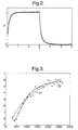
- the lens focus position drifts according to a trajectory given by Equation (1); lens cooling can be modelled with the same parameters. Starting from “cold”, the focus drift tends towards a saturation value at which an equilibrium is reached in which the rate at which energy received by the lens equals the rate at which the lens dissipates heat. Similarly, starting from warm, the focus position drifts toward its default value under conditions of no lens heating.
- a typical plot showing the lens heating and cooling focus drift trajectory is given in Figure 2. Along the horizontal and vertical axes the time T and the drift F are plotted, respectively, in arbitrary units.
- a heating phase is first performed during which the lens is heated (by the exposure radiation) continuously for two hours with fully opened reticle masking blades (defined below) and no reticle present.
- the reticle masking blades are a shuttering system interposed at some location in the radiation path to define the illumination field, i.e. the size and shape of the beam incident on the reticle.
- the heating is done with a wafer coated with photoresist on the wafer table to take into account the effect of wafer reflectivity.
- a coarse calibration is then done whereby the best focus position is measured, using for example a limited number of TIS markers, while the lens cools down and the focus drift returns to its default position.
- the focus position can be measured using so-called actinic alignment, in which the exposure radiation is directly used, but only briefly to avoid further heating effects.
- an attenuator can be used to reduce the intensity of the exposure radiation during the measurements, to further prevent lens heating during the measurements.
- a so-called red alignment technique can be used in which a different radiation, such as red light from a helium neon laser is used in a through-the-lens (TTL) technique to determine the best focus position, but without lens heating. Appropriate corrections can be made, if necessary, to account for the fact that the alignment radiation may have a different wavelength from the exposure radiation.
- cooling measurements are done every 30 seconds on any of five TIS markers on the x -axis and four off-axis markers (two with positive y -coordinate and two with negative y -coordinate).
- the fit is considered satisfactory if the residue is less than 30 nm, which indicates that the (image sensor) measurements are reliably within a 99.7% confidence interval.
- the two time constants have been found usually to have a value between 180 and 530 seconds, and 750 and 1220 seconds, respectively. These time constants are quite well found by this coarse calibration, but a fine calibration is preferably performed to obtain better values for the scaling factors.
- a fine calibration is preferably performed to obtain better values for the scaling factors.
- One reason why the scaling factors are not so accurately found by the coarse calibration is that during the heating phase, the wafer has been continuously exposed for two hours, which causes the reflectivity of the photoresist to increase, which results in the scaling factor being overestimated.
- Estimates for the time constants resulting from coarse calibration can subsequently be used as a basis for fine calibration, even at different illumination settings.
- the step of fine calibration may be referred to hereafter as "fine tuning" as well.
- one coarse calibration measurement could be done at one illumination setting, followed by several fine tuning tests at different illumination settings, to obtain the different values of the scaling factors for the different illumination settings.
- the time constants obtained from the coarse calibration are, in this embodiment, used at all other settings, assuming that by measuring the focus every 30 seconds the dynamic behaviour is modelled sufficiently well so that errors in the time constants have only a small impact on the focus drift.
- the fact that the dynamic behaviour is substantially an intrinsic lens characteristic, independent of the amount of energy received by the lens, supports said assumption.
- the fine tuning measurements are made, according to this embodiment, using the FOCAL technique described above using exposures on wafers.
- TIS can be used to measure lens-heating-induced effects. Both methods use alternate dummy heating exposures and measurements (measurement exposures in the case of FOCAL and direct measurements of the aerial image in the case of TIS). The dummy exposures are done to (successively) heat up the lens a little bit further, and the TIS scans/FOCAL exposures are done to determine an aberration effect (such as, for example focus drift) at that particular stage in the lens heating trajectory. This alternately exposing and measuring is done for a specified period of time, usually in the range of from 30 to 120 minutes.
- a lens heating database is built up which stores the parameter values needed to correct for lens heating, and which in this embodiment consist of two time constants ( ⁇ 1 and ⁇ 2 ) and two scaling factors ( ⁇ 1 and ⁇ 2 ).
- a set of these parameters can be stored for each reticle and illumination setting of interest.
- a calculation for each type of aberration effect will give the predicted additional amount of that aberration effect resulting from lens-heating, over and above any intrinsic aberration effect, i.e. the default value for the lens.
- the correction to make to the lithographic projection apparatus to further compensate for the lens heating effect depends on each particular type of aberration effect according to table 1, for example.
- the correction can be performed automatically by the machine, based on tabulated or calculated values relating the magnitude of the aberration effect to the size of the mechanical adjustment necessary. Saddle-like deformation of one or more lens elements to correct for particular aberrations is described, for example, in PCT publication WO 99/67683, incorporated herein by reference.
- an accurate estimate of all the model parameters is obtained with a single (fine) calibration step.
- An advantage of this embodiment is the reduction of cycle time in a calibration sequence with respect to the cycle time required for a calibration sequence comprising a coarse and a fine calibration.
- Characteristic of the embodiment is the method of fitting the model data to the measured fine tune data. The fit-method yields accurate estimates for the time constants as well as the scaling factors. For a given set of time constants ⁇ 1 and ⁇ 2 , an estimate for ⁇ 1 and ⁇ 2 and the corresponding residue R can be found in the same way as in the fine calibration step of the first embodiment.
- the residue R depends on the particular values used for the set of time constants.
- the first set of time ranges defined by the differences ⁇ 1 n - ⁇ 11 and ⁇ 2 n - ⁇ 21 , denoted by TR11 and TR12, respectively, are chosen such that the actual values of ⁇ 1 and ⁇ 2 lie within these ranges (the choice may be based, for example, on previous empirical evidence or a previous coarse calibration).
- the scaling factors can be found using the method described in the first embodiment.
- the residues R ij are stored in a corresponding matrix addressable memory.
- the smallest residue in this matrix now represents the best fit, and the corresponding estimates for ⁇ 1 and ⁇ 2 are denoted here by ⁇ 1 est 1 and ⁇ 2 est 1 .
- the time ranges TR21 and TR22 are 800 seconds.
- the steps described above can be repeated to yield a second improved estimate for the time constants denoted by ⁇ 1 est 2 and ⁇ 2 est 2 .
- two more successive steps of increasing accuracy are performed, resulting in a fourth estimate ⁇ 1 est 4 and ⁇ 2 est 4 for respectively ⁇ 1 and ⁇ 2 , based on a time resolution of 1.6 seconds.
- FIG 3 a typical example of the aberration effect "magnification drift” is shown.
- the stars indicate measured magnification drift as a function of time, due to lens heating.
- the graph 31 is a plot of predicted magnification drift, based on a coarse and fine calibration method as described in the first embodiment.
- Graph 32 is a plot of magnification drift as predicted by parameters obtained by the method according to the present embodiment.
- the residue for the prediction 32 is approximately three times smaller than the residue for the prediction 31.
- the lens heating effect will generally be different for each illumination setting such as numerical aperture, sigma-setting, and whether the illumination mode intensity distribution is disc-like, annular or multi-polar, for example. This is because the amount of light and the shape of the light beam going through the lens differs for each setting. This causes the lens elements to be heated differently and therefore influences the contribution of lens heating to each type of aberration.
- NAill NA ⁇ inner + ⁇ outer 2
- An equivalent value for NAill can be obtained for multipolar modes, such as quadrupolar. It has been found empirically that both the scaling factors ⁇ 1 and ⁇ 2 of the model of Equations (1) and (2) depend linearly on the value of NAill, ranging from maximum at the lowest NAill to a value approximately three to five times smaller at the highest NAill.
- the absolute values depend on the lens type and also show small differences between lenses of the same type.
- the scaling factors can be measured for a particular lens or machine at, for example, three different NAill settings, preferably at two extreme settings and one intermediate setting.
- the slope of the dependency of the scaling factors on NAill value can then be obtained by a linear fit, and then, when operating the machine at a NAill setting for which it has not been calibrated, the scaling factors can be linearly interpolated based on this slope from the known scaling factors at the measured NAill settings.
- This linear NAill-dependency is an empirical approximation. Depending on the accuracy required, more calibrations at intermediate settings or even non-linear NAill-dependencies can be used.
- the wafer During exposures, the wafer reflects some of the light back into the lens. This will have a certain effect on lens heating, and thus aberration effects during exposure of a batch, depending on the intensity of the reflected light.
- the intensity of the radiation reflected from the wafer depends on a number of factors:
- the present embodiment it is possible to adjust for the effect of a wafer reflectivity different from that present during the calibration process.
- the fine tuning test is repeated using a substrate of the new wafer material with no patterns or structures, but with the photoresist type and thickness as used for the standard fine tuning calibration measurements.
- a correction factor Cf can be calculated by dividing the total focus drift (or total drift in any desired aberration effect) at saturation with the new substrate by the calibration measurement focus drift (or other desired aberration drift).
- the projection system may be in a condition where heat-induced aberration effects are substantially absent.
- a change of aberration effect is typically largest during successive exposures of target portions of the first wafer of said batch.
- adjustments as determined and applied according to the previous embodiments also typically are largest during the irradiation of target portions of the first wafer.
- relatively large adjustments may not be as accurate as smaller adjustments. Consequently, resulting residual aberration effects tend to be most pronounced in the patterned layer on said first wafer. This is called the "first-wafer-effect".
- the first-wafer-effect is alleviated by supplying the projection beam to the projection system during a period of time T preheat just preceding the start of exposures of target portions of the first wafer.
- a pre-heating of the projection lens as discussed here is of particular relevance for a manufacturing process run on a multiple-stage lithographic projection apparatus.
- the pre-heating of the lens can be performed while the first wafer is subjected to preparatory steps. During these steps there is no wafer at the exposure position, and therefore, the pre-heating has no impact on the processing time of the batch (i.e. it has no impact on throughput).
- the invention may be used for the projection system of a lithographic apparatus and in any other type of imaging system in which lens aberrations as a result of lens heating are to be compensated.
- the embodiments described above are in terms of correction of lens aberrations which occur or worsen as a result of lens heating effects, the invention is also applicable to other corrections, such as those resulting from radiative compaction of lens elements, quantum and/or atomic effects in the lens, creep, general ageing of the lens and so on; the appended claims also encompass these effects.
- the invention is also not limited to lens-dependent effects, but is applicable to changes in other components, such as reticle effects, whether caused by heating or otherwise.
Landscapes
- Physics & Mathematics (AREA)
- General Physics & Mathematics (AREA)
- Health & Medical Sciences (AREA)
- Life Sciences & Earth Sciences (AREA)
- Atmospheric Sciences (AREA)
- Toxicology (AREA)
- Engineering & Computer Science (AREA)
- Environmental & Geological Engineering (AREA)
- Epidemiology (AREA)
- Public Health (AREA)
- Exposure And Positioning Against Photoresist Photosensitive Materials (AREA)
- Exposure Of Semiconductors, Excluding Electron Or Ion Beam Exposure (AREA)
Priority Applications (1)
| Application Number | Priority Date | Filing Date | Title |
|---|---|---|---|
| EP01305099A EP1164436A3 (fr) | 2000-06-14 | 2001-06-12 | Opération d'un appareil de projection lithographique |
Applications Claiming Priority (3)
| Application Number | Priority Date | Filing Date | Title |
|---|---|---|---|
| EP00305029 | 2000-06-14 | ||
| EP00305029 | 2000-06-14 | ||
| EP01305099A EP1164436A3 (fr) | 2000-06-14 | 2001-06-12 | Opération d'un appareil de projection lithographique |
Publications (2)
| Publication Number | Publication Date |
|---|---|
| EP1164436A2 true EP1164436A2 (fr) | 2001-12-19 |
| EP1164436A3 EP1164436A3 (fr) | 2005-01-05 |
Family
ID=26073198
Family Applications (1)
| Application Number | Title | Priority Date | Filing Date |
|---|---|---|---|
| EP01305099A Ceased EP1164436A3 (fr) | 2000-06-14 | 2001-06-12 | Opération d'un appareil de projection lithographique |
Country Status (1)
| Country | Link |
|---|---|
| EP (1) | EP1164436A3 (fr) |
Cited By (7)
| Publication number | Priority date | Publication date | Assignee | Title |
|---|---|---|---|---|
| EP1496397A1 (fr) * | 2003-07-11 | 2005-01-12 | ASML Netherlands B.V. | Procédé et système de correction anticipé de type overlay de distortion et décalage induits par un motif, et appareil de projection lithographique utilisant ces procédé et système |
| EP1626310A1 (fr) * | 2004-07-08 | 2006-02-15 | ASML Netherlands B.V. | Appareil lithographique et méthode pour la fabrication d'un dispositif |
| US7102728B2 (en) | 2002-02-27 | 2006-09-05 | Nikon Corporation | Imaging optical system evaluation method, imaging optical system adjustment method, exposure apparatus and exposure method |
| US7262831B2 (en) | 2004-12-01 | 2007-08-28 | Asml Netherlands B.V. | Lithographic projection apparatus and device manufacturing method using such lithographic projection apparatus |
| US8715909B2 (en) | 2007-10-05 | 2014-05-06 | Infineon Technologies Ag | Lithography systems and methods of manufacturing using thereof |
| US9885656B2 (en) | 2014-12-17 | 2018-02-06 | Kla-Tencor Corporation | Line scan knife edge height sensor for semiconductor inspection and metrology |
| TWI681260B (zh) * | 2016-05-31 | 2020-01-01 | 上海微電子裝備(集團)股份有限公司 | 光刻機刀口組、大視場光刻機和曝光方法 |
Family Cites Families (3)
| Publication number | Priority date | Publication date | Assignee | Title |
|---|---|---|---|---|
| US5337097A (en) * | 1985-12-26 | 1994-08-09 | Nippon Kogaku K.K. | Projection optical apparatus |
| JPH05144701A (ja) * | 1991-11-22 | 1993-06-11 | Canon Inc | 投影露光装置及びそれを用いた半導体素子の製造方法 |
| JP3412981B2 (ja) * | 1995-08-29 | 2003-06-03 | キヤノン株式会社 | 投影露光装置および投影露光方法 |
-
2001
- 2001-06-12 EP EP01305099A patent/EP1164436A3/fr not_active Ceased
Cited By (11)
| Publication number | Priority date | Publication date | Assignee | Title |
|---|---|---|---|---|
| US7102728B2 (en) | 2002-02-27 | 2006-09-05 | Nikon Corporation | Imaging optical system evaluation method, imaging optical system adjustment method, exposure apparatus and exposure method |
| EP1496397A1 (fr) * | 2003-07-11 | 2005-01-12 | ASML Netherlands B.V. | Procédé et système de correction anticipé de type overlay de distortion et décalage induits par un motif, et appareil de projection lithographique utilisant ces procédé et système |
| EP1626310A1 (fr) * | 2004-07-08 | 2006-02-15 | ASML Netherlands B.V. | Appareil lithographique et méthode pour la fabrication d'un dispositif |
| KR100795140B1 (ko) | 2004-07-08 | 2008-01-17 | 에이에스엠엘 네델란즈 비.브이. | 리소그래피 투영장치 및 상기 리소그래피 투영장치를 사용하는 디바이스 제조방법 |
| US7403264B2 (en) | 2004-07-08 | 2008-07-22 | Asml Netherlands B.V. | Lithographic projection apparatus and a device manufacturing method using such lithographic projection apparatus |
| EP1975723A1 (fr) | 2004-07-08 | 2008-10-01 | ASML Netherlands B.V. | Appareil de projection lithographique et procédé de fabrication de dispositif utilisant un appareil de projection lithographique |
| US7626684B2 (en) | 2004-07-08 | 2009-12-01 | Asml Netherlands B.V. | Lithographic projection apparatus and a device manufacturing method using such lithographic projection apparatus |
| US7262831B2 (en) | 2004-12-01 | 2007-08-28 | Asml Netherlands B.V. | Lithographic projection apparatus and device manufacturing method using such lithographic projection apparatus |
| US8715909B2 (en) | 2007-10-05 | 2014-05-06 | Infineon Technologies Ag | Lithography systems and methods of manufacturing using thereof |
| US9885656B2 (en) | 2014-12-17 | 2018-02-06 | Kla-Tencor Corporation | Line scan knife edge height sensor for semiconductor inspection and metrology |
| TWI681260B (zh) * | 2016-05-31 | 2020-01-01 | 上海微電子裝備(集團)股份有限公司 | 光刻機刀口組、大視場光刻機和曝光方法 |
Also Published As
| Publication number | Publication date |
|---|---|
| EP1164436A3 (fr) | 2005-01-05 |
Similar Documents
| Publication | Publication Date | Title |
|---|---|---|
| US6563564B2 (en) | Method of operating an optical imaging system, lithographic projection apparatus, device manufacturing method, and device manufactured thereby | |
| EP1626310B1 (fr) | Appareil lithographique et méthode pour la fabrication d'un dispositif | |
| US7262831B2 (en) | Lithographic projection apparatus and device manufacturing method using such lithographic projection apparatus | |
| US6977714B2 (en) | Lithographic manufacturing process, lithographic projection apparatus, and device manufactured thereby | |
| US6646729B2 (en) | Method of measuring aberration in an optical imaging system | |
| US7221430B2 (en) | Lithographic apparatus and device manufacturing method | |
| US20030047694A1 (en) | Method of measuring aberration of a projection system of a lithographic apparatus, device manufacturing method, and device manufactured thereby | |
| EP2063321A2 (fr) | Procédé de mesure de focus d'un appareil de projection lithographique | |
| EP1868034A1 (fr) | Capteur de front d'onde doté d'un filtre gris et appareil lithographique le comprenant | |
| US7177010B2 (en) | Lithographic apparatus and device manufacturing method | |
| US7596420B2 (en) | Device manufacturing method and computer program product | |
| EP1128217B1 (fr) | Méthode de mesure des aberrations dans un système optique de formation d'image | |
| EP1580605B1 (fr) | Méthode de détermination d'aberration d'un système de projection d'un appareil lithographique. | |
| US6987555B2 (en) | Lithographic apparatus, device manufacturing method, and device manufactured thereby | |
| EP1164436A2 (fr) | Opération d'un appareil de projection lithographique | |
| US7084952B2 (en) | Lithographic apparatus, device manufacturing method, and computer-readable storage medium | |
| US9423701B2 (en) | Lithographic method and assembly | |
| US7619717B2 (en) | Method for performing a focus test and a device manufacturing method | |
| US6897947B1 (en) | Method of measuring aberration in an optical imaging system | |
| EP1248154A1 (fr) | Procédé de fabrication lithographique et appareil de projection lithographique | |
| EP1286223B1 (fr) | Méthode de mesure de l'aberration d'un système de projection lithographique | |
| US6788383B1 (en) | Lithographic apparatus, device manufacturing methods, and computer-readable storage medium |
Legal Events
| Date | Code | Title | Description |
|---|---|---|---|
| PUAI | Public reference made under article 153(3) epc to a published international application that has entered the european phase |
Free format text: ORIGINAL CODE: 0009012 |
|
| AK | Designated contracting states |
Kind code of ref document: A2 Designated state(s): AT BE CH CY DE DK ES FI FR GB GR IE IT LI LU MC NL PT SE TR |
|
| AX | Request for extension of the european patent |
Free format text: AL;LT;LV;MK;RO;SI |
|
| RAP1 | Party data changed (applicant data changed or rights of an application transferred) |
Owner name: ASML NETHERLANDS B.V. |
|
| RAP1 | Party data changed (applicant data changed or rights of an application transferred) |
Owner name: ASML NETHERLANDS B.V. |
|
| PUAL | Search report despatched |
Free format text: ORIGINAL CODE: 0009013 |
|
| AK | Designated contracting states |
Kind code of ref document: A3 Designated state(s): AT BE CH CY DE DK ES FI FR GB GR IE IT LI LU MC NL PT SE TR |
|
| AX | Request for extension of the european patent |
Extension state: AL LT LV MK RO SI |
|
| 17P | Request for examination filed |
Effective date: 20050610 |
|
| AKX | Designation fees paid |
Designated state(s): DE FR GB IT NL |
|
| STAA | Information on the status of an ep patent application or granted ep patent |
Free format text: STATUS: THE APPLICATION HAS BEEN REFUSED |
|
| 18R | Application refused |
Effective date: 20090717 |