EP1128428A2 - Procédé de fabrication d'un dispositif semi-conducteur - Google Patents
Procédé de fabrication d'un dispositif semi-conducteur Download PDFInfo
- Publication number
- EP1128428A2 EP1128428A2 EP01104254A EP01104254A EP1128428A2 EP 1128428 A2 EP1128428 A2 EP 1128428A2 EP 01104254 A EP01104254 A EP 01104254A EP 01104254 A EP01104254 A EP 01104254A EP 1128428 A2 EP1128428 A2 EP 1128428A2
- Authority
- EP
- European Patent Office
- Prior art keywords
- oxide layer
- capacitor
- layer
- oxide
- doping
- Prior art date
- Legal status (The legal status is an assumption and is not a legal conclusion. Google has not performed a legal analysis and makes no representation as to the accuracy of the status listed.)
- Granted
Links
Images

Classifications
-
- H—ELECTRICITY
- H10—SEMICONDUCTOR DEVICES; ELECTRIC SOLID-STATE DEVICES NOT OTHERWISE PROVIDED FOR
- H10B—ELECTRONIC MEMORY DEVICES
- H10B12/00—Dynamic random access memory [DRAM] devices
-
- H—ELECTRICITY
- H10—SEMICONDUCTOR DEVICES; ELECTRIC SOLID-STATE DEVICES NOT OTHERWISE PROVIDED FOR
- H10B—ELECTRONIC MEMORY DEVICES
- H10B53/00—Ferroelectric RAM [FeRAM] devices comprising ferroelectric memory capacitors
-
- H—ELECTRICITY
- H10—SEMICONDUCTOR DEVICES; ELECTRIC SOLID-STATE DEVICES NOT OTHERWISE PROVIDED FOR
- H10B—ELECTRONIC MEMORY DEVICES
- H10B53/00—Ferroelectric RAM [FeRAM] devices comprising ferroelectric memory capacitors
- H10B53/30—Ferroelectric RAM [FeRAM] devices comprising ferroelectric memory capacitors characterised by the memory core region
-
- H—ELECTRICITY
- H10—SEMICONDUCTOR DEVICES; ELECTRIC SOLID-STATE DEVICES NOT OTHERWISE PROVIDED FOR
- H10D—INORGANIC ELECTRIC SEMICONDUCTOR DEVICES
- H10D1/00—Resistors, capacitors or inductors
- H10D1/60—Capacitors
- H10D1/68—Capacitors having no potential barriers
- H10D1/682—Capacitors having no potential barriers having dielectrics comprising perovskite structures
-
- H—ELECTRICITY
- H10—SEMICONDUCTOR DEVICES; ELECTRIC SOLID-STATE DEVICES NOT OTHERWISE PROVIDED FOR
- H10P—GENERIC PROCESSES OR APPARATUS FOR THE MANUFACTURE OR TREATMENT OF DEVICES COVERED BY CLASS H10
- H10P95/00—Generic processes or apparatus for manufacture or treatments not covered by the other groups of this subclass
-
- H—ELECTRICITY
- H10—SEMICONDUCTOR DEVICES; ELECTRIC SOLID-STATE DEVICES NOT OTHERWISE PROVIDED FOR
- H10B—ELECTRONIC MEMORY DEVICES
- H10B12/00—Dynamic random access memory [DRAM] devices
- H10B12/01—Manufacture or treatment
- H10B12/02—Manufacture or treatment for one transistor one-capacitor [1T-1C] memory cells
- H10B12/03—Making the capacitor or connections thereto
- H10B12/033—Making the capacitor or connections thereto the capacitor extending over the transistor
- H10B12/0335—Making a connection between the transistor and the capacitor, e.g. plug
Definitions
- the invention relates to a method for producing a Semiconductor component according to the preamble of the claims 1 and 2.
- DRAMs microelectronic semiconductor memory devices
- a switching transistor essentially consist of a switching transistor and a storage capacitor.
- the saved Information is provided by the state of charge of the storage capacitor represents. Due to discharge processes the state of charge of a (volatile) DRAM memory cell are constantly renewed.
- capacitor dielectrics In DRAMs, oxide or nitride layers are usually used as capacitor dielectrics, which have a dielectric constant of at most about 8.
- "new" capacitor materials containing metal oxides (paraelectrics or ferroelectrics) with significantly higher dielectric constants are required.
- ferroelectric capacitor materials are SrBi 2 (Ta, Nb) 2 O 9 (SBT or SBTN), Pb (Zr, Ti) O 3 (PZT), Bi 4 Ti 3 O 12 (BTO), a well-known example of a paraelectric High epsylon capacitor material is (Ba, Sr) TiO 3 (BST).
- the invention has for its object a method for Specify manufacture of a semiconductor device in which a storage capacitor that is a ferroelectric or Paraelectric capacitor material used, sufficient is protected against the ingress of hydrogen.
- An essential aspect of the invention is that to protect against hydrogen intrusion into the Capacitor material is an oxide layer with a barrier material is endowed. Due to the barrier substance atoms introduced into the oxide layer the doped oxide layer becomes largely impermeable to hydrogen.
- claim 1 (First) doped oxide layer formed below the capacitor.
- claim 2 Another possibility (claim 2) is to deposit a thin (second) oxide layer over the capacitor and - at least in sections - to endow them.
- the barrier material is preferably nitrogen. In this case, doping becomes nitridization the first or second oxide layer.
- suitable substances e.g. Noble gases, can be used as a barrier material.
- the oxide layers are doped (or nitrided) with the help of a plasma discharge containing the barrier material.
- the plasma discharge enables that in short Time (about 60 s) a sufficiently high barrier substance concentration generated in the first and / or second oxide layer without a maximum substrate temperature in the range of 50-120 ° C must be exceeded.
- the plasma doping is therefore compatible with conventional photoresist masking techniques. Accordingly, an advantageous one is identified Process sequence in that before the plasma doping one on the first and / or second oxide layer Mask is applied, by means of which the doping of the Oxide layer is structured, and that subsequently an oxide etching step is carried out.
- the oxide etching of a contact hole with a previously applied (lacquer) mask an advantageous process variant in that the created structure one more time of plasma doping exposed with barrier fabric.
- the hole walls of the contact hole are doped (e.g. nitrided).
- the advantage of this measure is that now the hole walls of the contact hole do not pass hydrogen and can diffuse to the capacitor material. This is important because especially when the contact hole is subsequently filled, for example with tungsten (W), relatively large quantities released by hydrogen.
- the plasma doping can expediently either by a PIII (plasma immersion ion implantation) procedure or brought about by a PLAD (so-called plasma doping) process become. Both of the methods mentioned enable the targeted Setting an isotropic ("plasma cloud”) and an anisotropic (“Ballistic implantation") doping component in Dependence on the selected process parameters. By the increase in the isotropic doping component can be, for example also irregular surface topologies (e.g. Trenches, holes, etc.) evenly doped.
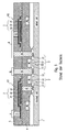
- the two Construction concepts have in common that a switching transistor S1, S2 in a lower level directly on a semiconductor substrate 1 is formed and a storage capacitor K1, K2 in an upper level is arranged, the two levels by an intermediate insulation layer 4 from each other are separated.
- the Switching transistor S1 and the storage capacitor Kl essentially arranged directly one above the other, the lower electrode 31 of the storage capacitor S1 via a with a conductive Material filled contact hole 41 ("plug") with a Drain region 21 of the MOS transistor S1, 2 through the insulation layer 4 is electrically connected therethrough.
- offset cell the Switching transistor S2 and the storage capacitor K2 from each other offset, the upper electrode 33 of the Storage capacitor K2 through two contact holes with the Drain region 21 of the MOS transistor S2, 2 electrically connected is.
- the drain region 21 and a source region 23 are formed between which there is a channel, which by a gate 22 arranged above the channel in its conductivity can be controlled.
- the gate 22 can by a Word line WL of the memory component formed or with this be connected.
- the source region 23 is with a bit line BL of the memory device connected.
- the MOS transistor 2 is then connected to the planarizing Insulation layer, for example a first oxide layer 4, covered.
- a storage capacitor 3 is placed on the first oxide layer 4 shaped.
- the contact hole 41 etched and with a conductive Material, for example polycrystalline silicon, filled.
- a conductive Material for example polycrystalline silicon
- a dielectric layer 32 of a ferroelectric or paraelectric material is deposited on the lower electrode 31.
- the dielectric layer 32 forms the capacitor dielectric.
- An upper electrode 33 is deposited over the entire surface above the dielectric layer 32.
- the structure obtained is finally covered with a further planarizing insulation layer 5, for example also consisting of SiO 2 .
- the source region 23 of the MOS transistor 2 connected to the bit line BL by one through both Insulation layers 4 and 5 extending contact hole 45 are formed and filled with a conductive material.
- Contact hole 46 is formed around the drain region 21 of the MOS transistor S2 by means of a conductive cross connection 8 and another extending through the upper insulation layer 5 Contact hole 52 with the upper electrode 33 of the Storage capacitor S2, 2 to connect.
- the oxide layer 4 is subsequently through CMP (chemical mechanical polishing) planarized.
- the oxide layer 4 is covered with a Paint mask layer covered, which then e.g. on photolithographic Ways is structured. It is for this made sure that at the point where the contact hole later 46 is to be formed, a mask structure 6 remains.
- the nitridization step takes place at a substrate temperature of 50 to a maximum of 120 ° C and is therefore compatible with the photomask technology used.
- the plasma nitridation causes that outside of the Mask structure 6 in a near-surface area nitrogen atoms be built into the first oxide layer 4.
- the nitridized surface area of the first created in this way Oxide layer 4 is designated by reference number 7A.
- the lower Pt electrode is used first 31 on the nitrided surface area 7A of FIG first oxide layer 4 applied.
- the dielectric, in particular para- or ferroelectric layer 32 consisting for example of BST or other suitable material such as. SBTN, PZT, BTO etc., deposited.
- the upper layer is then applied to the dielectric layer 32 Pt electrode 33 deposited and together with the dielectric Layer 32 by photolithography and etching technology structured.
- the deposition and structuring of the dielectric Layer 32 and the upper Pt electrode 33 takes place preferably such that both layers are at least on each other one side of the lower electrode 31 in the lateral direction extend beyond this and in the form of a step on the lower electrode 31 abut. Through the step area the effective capacitor area increases.
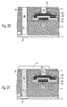
- This structure is then coated with a thin second oxide layer consisting, for example, of SiO 2 .
- the following are suitable on the second oxide layer Place photoresist mask structures by lithography 9.1 and 9.2 generated.
- the mask structure 9.2 is preferred attached centrally above the storage capacitor K2.
- the mask structure 9.1 covers an area of the second oxide layer, which is immediately above the non-nitrided Region of the first nitrided oxide layer 7A.
- the thin second oxide layer then also becomes one Subjected to plasma nitridation.
- the second oxide layer and those used in nitridization Process parameters are used in their entirety Thick or nitrided only in a near-surface area.
- the nitridized one shown in FIG. 2B is thereby second oxide layer 7B formed, which below the photoresist mask structures 9.1 and 9.2 still made of non-nitrided Oxide material.
- planarizing upper insulation layer 5 preferably also an SiO 2 layer, is then deposited over the structure described. In this process, which can take place with the participation of hydrogen, the capacitor 3 is already protected by the second nitridized oxide layer 7B.
- the two contact holes 46 and 52 are then etched. Because of the one generated by the masking 6, 9.1 and 9.2 Structuring of the nitrided oxide layers 7A and 7B can both vias 46 and 52 by conventional oxide etching be formed. An etching different Layer materials are not required. Hence point the contact holes 46 and 52 very dimensionally stable and flat Inner wall surfaces, causing a lateral reduction in structure is favored.
- the contact holes 46, 52 can together in a single etching step or in two individual etching steps are formed.
- a third plasma nitridation step can now be carried out be performed. Thereby, near-surface inner wall surface areas 7C of the two contact holes 46 and 52 and nitriding a surface area of the upper oxide layer 5.
- the contact holes 46 and 52 are then in that already described Way with a suitable conductive material, for example W, filled. After that, a not shown Do a CMP step to create a planar surface be performed.
- the PIII process is usually carried out in one of two chambers existing plant.
- one chamber becomes a constantly burning nitrogen plasma of a high Generates plasma density.
- a magnetic field can be used.
- the substrate with the oxide layers to be nitrided is located yourself in the other chamber.
- the two chambers are through a pinhole connected together. It will now be for short Time a voltage is applied to the substrate, creating nitrogen ions extracted from the plasma through the pinhole accelerated to the substrate 1 and in the respective exposed Oxide layer are braked.
- the degree of anisotropy of nitriding can be greatly influenced become.
- anisotropic ion implantation For example, by humiliating the Extraction voltage, increase in plasma density as well a change in the geometric relationships can be achieved be that the nitridization by an extended "Plasma cloud" is effected. In this case it is an even one Nitridization of the oxide layers even with irregular ones Surface topologies achievable and it has been shown that contact holes with an opening ratio up to about 1:12 can be nitrided in full length without problems.
- the PLAD process is usually done in a single Plasma chamber performed.
- the system is similar to a sputter system built up. One is between two electrodes High frequency voltage applied and a nitrogen plasma ignited. The substrate is on the electrode towards which the nitrogen ions are accelerated.
- the System works like a reversed polarity sputter system.
- the degree of anisotropy of nitridization can also be used in the PLAD process through the system geometry and configuration of the nitrogen plasma can be set as desired.
- a typical nitridation dose in the range from 10 19 to 10 22 atoms / cm 2 can be set with both methods.
- Typical nitridization energies (kinetic energy of the accelerated nitrogen ions when they hit the oxide layers) are in the range of 1 to 12 keV.
- the nitridation process then begins at the highest nitridation energy and ends at the lowest nitridization energy.
- the duration of the entire nitriding step is typically about 60 seconds at a nitriding dose of 10 20 atoms / cm 2 .
Landscapes
- Semiconductor Memories (AREA)
- Formation Of Insulating Films (AREA)
- Semiconductor Integrated Circuits (AREA)
Applications Claiming Priority (2)
| Application Number | Priority Date | Filing Date | Title |
|---|---|---|---|
| DE10010284 | 2000-02-25 | ||
| DE10010284A DE10010284C2 (de) | 2000-02-25 | 2000-02-25 | Verfahren zur Herstellung eines Halbleiterbauelements mit einem Kondensator |
Publications (3)
| Publication Number | Publication Date |
|---|---|
| EP1128428A2 true EP1128428A2 (fr) | 2001-08-29 |
| EP1128428A3 EP1128428A3 (fr) | 2004-10-27 |
| EP1128428B1 EP1128428B1 (fr) | 2007-10-31 |
Family
ID=7633315
Family Applications (1)
| Application Number | Title | Priority Date | Filing Date |
|---|---|---|---|
| EP01104254A Expired - Lifetime EP1128428B1 (fr) | 2000-02-25 | 2001-02-22 | Procédé de fabrication d'un dispositif semi-conducteur |
Country Status (7)
| Country | Link |
|---|---|
| US (1) | US6316275B2 (fr) |
| EP (1) | EP1128428B1 (fr) |
| JP (1) | JP3990542B2 (fr) |
| KR (1) | KR100397881B1 (fr) |
| CN (1) | CN1174472C (fr) |
| DE (2) | DE10065976A1 (fr) |
| TW (1) | TW502399B (fr) |
Cited By (1)
| Publication number | Priority date | Publication date | Assignee | Title |
|---|---|---|---|---|
| EP1653514A4 (fr) * | 2003-05-27 | 2010-07-21 | Panasonic Corp | Dispositif semiconducteur et procede de production associe |
Families Citing this family (23)
| Publication number | Priority date | Publication date | Assignee | Title |
|---|---|---|---|---|
| DE10121657B4 (de) * | 2001-05-03 | 2010-02-11 | Qimonda Ag | Mikroelektronische Struktur mit Wasserstoffbarrierenschicht |
| US7037730B2 (en) * | 2001-07-11 | 2006-05-02 | Micron Technology, Inc. | Capacitor with high dielectric constant materials and method of making |
| JP2003152165A (ja) * | 2001-11-15 | 2003-05-23 | Fujitsu Ltd | 半導体装置およびその製造方法 |
| US7270573B2 (en) * | 2002-08-30 | 2007-09-18 | Fci Americas Technology, Inc. | Electrical connector with load bearing features |
| TWI229935B (en) | 2002-11-13 | 2005-03-21 | Matsushita Electric Industrial Co Ltd | Semiconductor device and method for fabricating the same |
| JP4636834B2 (ja) * | 2002-11-13 | 2011-02-23 | パナソニック株式会社 | 半導体装置及びその製造方法 |
| US7101785B2 (en) * | 2003-07-22 | 2006-09-05 | Infineon Technologies Ag | Formation of a contact in a device, and the device including the contact |
| JP2005229001A (ja) | 2004-02-16 | 2005-08-25 | Toshiba Corp | 半導体装置及び半導体装置の製造方法 |
| JP4049119B2 (ja) * | 2004-03-26 | 2008-02-20 | セイコーエプソン株式会社 | 強誘電体メモリ素子の製造方法 |
| US20050239219A1 (en) * | 2004-04-26 | 2005-10-27 | Moon Bum-Ki | Process for fabrication of a ferrocapacitor with a large effective area |
| JP4803995B2 (ja) * | 2004-06-28 | 2011-10-26 | 富士通セミコンダクター株式会社 | 半導体装置及びその製造方法 |
| JP4042730B2 (ja) * | 2004-09-02 | 2008-02-06 | セイコーエプソン株式会社 | 強誘電体メモリおよびその製造方法 |
| JP2006186245A (ja) * | 2004-12-28 | 2006-07-13 | Tokyo Electron Ltd | トンネル酸化膜の窒化処理方法、不揮発性メモリ素子の製造方法および不揮発性メモリ素子、ならびにコンピュータプログラムおよび記録媒体 |
| JP2006222389A (ja) * | 2005-02-14 | 2006-08-24 | Toshiba Corp | 半導体記憶装置及びその製造方法 |
| JP4953580B2 (ja) * | 2005-03-03 | 2012-06-13 | 富士通セミコンダクター株式会社 | 半導体装置の製造方法 |
| US7927948B2 (en) | 2005-07-20 | 2011-04-19 | Micron Technology, Inc. | Devices with nanocrystals and methods of formation |
| JP2007067066A (ja) | 2005-08-30 | 2007-03-15 | Toshiba Corp | 半導体装置とその製造方法 |
| JP4935680B2 (ja) * | 2005-11-25 | 2012-05-23 | 富士通セミコンダクター株式会社 | 半導体装置の製造方法 |
| JP2006157062A (ja) * | 2006-03-10 | 2006-06-15 | Toshiba Corp | 半導体装置及び半導体装置の製造方法 |
| JP4567026B2 (ja) * | 2007-05-24 | 2010-10-20 | 富士通セミコンダクター株式会社 | 半導体装置の製造方法 |
| KR101481574B1 (ko) * | 2008-02-13 | 2015-01-14 | 삼성전자주식회사 | 반도체 소자의 제조 방법 |
| US10128016B2 (en) * | 2016-01-12 | 2018-11-13 | Asml Netherlands B.V. | EUV element having barrier to hydrogen transport |
| US20230097184A1 (en) * | 2021-09-24 | 2023-03-30 | Intel Corporation | Integrated circuits with high dielectric constant interfacial layering |
Family Cites Families (8)
| Publication number | Priority date | Publication date | Assignee | Title |
|---|---|---|---|---|
| JP3131982B2 (ja) | 1990-08-21 | 2001-02-05 | セイコーエプソン株式会社 | 半導体装置、半導体メモリ及び半導体装置の製造方法 |
| JP3063606B2 (ja) | 1996-02-13 | 2000-07-12 | 日本電気株式会社 | 半導体装置の製造方法 |
| EP0847079A3 (fr) | 1996-12-05 | 1999-11-03 | Texas Instruments Incorporated | Méthode de fabrication d'une électrode MIS |
| EP0862203A1 (fr) * | 1997-01-31 | 1998-09-02 | Texas Instruments Incorporated | Procédé pour fabriquer une capacité semi-conductrice à mémoire |
| KR100269314B1 (ko) * | 1997-02-17 | 2000-10-16 | 윤종용 | 플라즈마처리를이용한반도체장치의커패시터제조방법 |
| JP3098474B2 (ja) * | 1997-10-31 | 2000-10-16 | 日本電気株式会社 | 半導体装置の製造方法 |
| US6008103A (en) | 1998-02-27 | 1999-12-28 | Siemens Aktiengesellschaft | Method for forming trench capacitors in an integrated circuit |
| US6225656B1 (en) * | 1998-12-01 | 2001-05-01 | Symetrix Corporation | Ferroelectric integrated circuit with protective layer incorporating oxygen and method for fabricating same |
-
2000
- 2000-02-25 DE DE10065976A patent/DE10065976A1/de not_active Ceased
-
2001
- 2001-02-09 TW TW090102893A patent/TW502399B/zh not_active IP Right Cessation
- 2001-02-22 DE DE50113179T patent/DE50113179D1/de not_active Expired - Lifetime
- 2001-02-22 EP EP01104254A patent/EP1128428B1/fr not_active Expired - Lifetime
- 2001-02-23 JP JP2001049279A patent/JP3990542B2/ja not_active Expired - Fee Related
- 2001-02-23 CN CNB011049421A patent/CN1174472C/zh not_active Expired - Fee Related
- 2001-02-24 KR KR10-2001-0009483A patent/KR100397881B1/ko not_active Expired - Fee Related
- 2001-02-26 US US09/793,351 patent/US6316275B2/en not_active Expired - Lifetime
Cited By (1)
| Publication number | Priority date | Publication date | Assignee | Title |
|---|---|---|---|---|
| EP1653514A4 (fr) * | 2003-05-27 | 2010-07-21 | Panasonic Corp | Dispositif semiconducteur et procede de production associe |
Also Published As
| Publication number | Publication date |
|---|---|
| TW502399B (en) | 2002-09-11 |
| KR100397881B1 (ko) | 2003-09-13 |
| JP2001291843A (ja) | 2001-10-19 |
| US20010021554A1 (en) | 2001-09-13 |
| DE50113179D1 (de) | 2007-12-13 |
| EP1128428B1 (fr) | 2007-10-31 |
| EP1128428A3 (fr) | 2004-10-27 |
| US6316275B2 (en) | 2001-11-13 |
| CN1174472C (zh) | 2004-11-03 |
| KR20010085573A (ko) | 2001-09-07 |
| CN1310468A (zh) | 2001-08-29 |
| JP3990542B2 (ja) | 2007-10-17 |
| DE10065976A1 (de) | 2002-02-21 |
Similar Documents
| Publication | Publication Date | Title |
|---|---|---|
| EP1128428B1 (fr) | Procédé de fabrication d'un dispositif semi-conducteur | |
| DE4402216C2 (de) | Halbleiterbauelement mit Kondensatoren und zu seiner Herstellung geeignetes Verfahren | |
| DE3916228C2 (de) | Halbleiterspeichervorrichtung mit Stapelkondensatorzellenstruktur und Verfahren zu ihrer Herstellung | |
| DE19829300B4 (de) | Ferroelektrische Speichereinrichtung mit elektrischer Verbindung zwischen einer unteren Kondensatorelektrode und einem Kontaktstopfen sowie Verfahren zu deren Herstellung | |
| DE69529942T2 (de) | Verfahren zur Herstellung eines Halbleiterbauelements mit einem kapazitiven Element | |
| DE10163345B4 (de) | Verfahren zur Herstellung eines Kondensators in einem Halbleiterbauelement | |
| DE10142580B4 (de) | Verfahren zur Herstellung einer Grabenstrukturkondensatoreinrichtung | |
| DE19838741A1 (de) | Kondensator und Verfahren zur Herstellung eines Kondensators | |
| DE10219123B4 (de) | Verfahren zur Strukturierung keramischer Schichten auf Halbleitersubstanzen mit unebener Topographie | |
| DE10146013A1 (de) | Halbleitervorrichtung und Verfahren zu ihrer Herstellung | |
| DE10228528B4 (de) | Diffusionssperrfilm und dessen Herstellungsverfahren, Halbleiterspeicher und dessen Herstellungsverfahren | |
| DE19712540C1 (de) | Herstellverfahren für eine Kondensatorelektrode aus einem Platinmetall | |
| DE19963500C2 (de) | Verfahren zum Herstellen einer strukturierten metalloxidhaltigen Schicht, insbesondere einer ferroelektrischen oder paraelektrischen Schicht | |
| DE10158706B4 (de) | Halbleitervorrichtung und Verfahren zu deren Herstellung | |
| EP1202333B1 (fr) | Condensateur de stockage, structures de contact et procédé de fabrication | |
| DE10053171C2 (de) | Verfahren zum Herstellen einer ferroelektrischen oder paraelektrischen metalloxidhaltigen Schicht und eines Speicherbauelements daraus | |
| DE10125370C1 (de) | Verfahren zur Herstellung einer integrierten Halbleiterschaltung mit einem stark polarisierbaren Dielektrikum oder Ferroelektrikum | |
| DE10022655C2 (de) | Verfahren zur Herstellung von Kondensatorstrukturen | |
| DE10010284C2 (de) | Verfahren zur Herstellung eines Halbleiterbauelements mit einem Kondensator | |
| DE10008617A1 (de) | Verfahren zur Herstellung einer ferroelektrischen Schicht | |
| DE102004022602A1 (de) | Verfahren zur Herstellung eines Grabenkondensators, Verfahren zur Herstellung einer Speicherzelle, Grabenkondensator und Speicherzelle | |
| EP1202332B1 (fr) | Structure de contact pour un condensateur ferro-électrique et procédé de sa fabrication | |
| DE10066082B4 (de) | Gezielte lokale Erzeugung von Öffnungen in einer Schicht | |
| DE10250872B4 (de) | Verfahren zur Herstellung einer Halbleiterstruktur mit mehreren Gate-Stapeln | |
| WO1998014992A1 (fr) | Procede de production d'un dispositif a semi-conducteur |
Legal Events
| Date | Code | Title | Description |
|---|---|---|---|
| PUAI | Public reference made under article 153(3) epc to a published international application that has entered the european phase |
Free format text: ORIGINAL CODE: 0009012 |
|
| AK | Designated contracting states |
Kind code of ref document: A2 Designated state(s): AT BE CH CY DE DK ES FI FR GB GR IE IT LI LU MC NL PT SE TR |
|
| AX | Request for extension of the european patent |
Free format text: AL;LT;LV;MK;RO;SI |
|
| PUAL | Search report despatched |
Free format text: ORIGINAL CODE: 0009013 |
|
| AK | Designated contracting states |
Kind code of ref document: A3 Designated state(s): AT BE CH CY DE DK ES FI FR GB GR IE IT LI LU MC NL PT SE TR |
|
| AX | Request for extension of the european patent |
Extension state: AL LT LV MK RO SI |
|
| RIC1 | Information provided on ipc code assigned before grant |
Ipc: 7H 01L 21/8246 B Ipc: 7H 01L 21/3105 B Ipc: 7H 01L 21/02 A |
|
| 17P | Request for examination filed |
Effective date: 20041123 |
|
| AKX | Designation fees paid |
Designated state(s): DE FR GB IE IT |
|
| GRAP | Despatch of communication of intention to grant a patent |
Free format text: ORIGINAL CODE: EPIDOSNIGR1 |
|
| GRAS | Grant fee paid |
Free format text: ORIGINAL CODE: EPIDOSNIGR3 |
|
| GRAA | (expected) grant |
Free format text: ORIGINAL CODE: 0009210 |
|
| AK | Designated contracting states |
Kind code of ref document: B1 Designated state(s): DE FR GB IE IT |
|
| RAP1 | Party data changed (applicant data changed or rights of an application transferred) |
Owner name: QIMONDA AG |
|
| REG | Reference to a national code |
Ref country code: GB Ref legal event code: FG4D Free format text: NOT ENGLISH |
|
| REG | Reference to a national code |
Ref country code: IE Ref legal event code: FG4D Free format text: LANGUAGE OF EP DOCUMENT: GERMAN |
|
| REF | Corresponds to: |
Ref document number: 50113179 Country of ref document: DE Date of ref document: 20071213 Kind code of ref document: P |
|
| GBT | Gb: translation of ep patent filed (gb section 77(6)(a)/1977) |
Effective date: 20080116 |
|
| REG | Reference to a national code |
Ref country code: IE Ref legal event code: FD4D |
|
| ET | Fr: translation filed | ||
| PLBE | No opposition filed within time limit |
Free format text: ORIGINAL CODE: 0009261 |
|
| STAA | Information on the status of an ep patent application or granted ep patent |
Free format text: STATUS: NO OPPOSITION FILED WITHIN TIME LIMIT |
|
| 26N | No opposition filed |
Effective date: 20080801 |
|
| PG25 | Lapsed in a contracting state [announced via postgrant information from national office to epo] |
Ref country code: IE Free format text: LAPSE BECAUSE OF FAILURE TO SUBMIT A TRANSLATION OF THE DESCRIPTION OR TO PAY THE FEE WITHIN THE PRESCRIBED TIME-LIMIT Effective date: 20071031 |
|
| PG25 | Lapsed in a contracting state [announced via postgrant information from national office to epo] |
Ref country code: IT Free format text: LAPSE BECAUSE OF NON-PAYMENT OF DUE FEES Effective date: 20080229 |
|
| REG | Reference to a national code |
Ref country code: FR Ref legal event code: PLFP Year of fee payment: 15 |
|
| PGFP | Annual fee paid to national office [announced via postgrant information from national office to epo] |
Ref country code: FR Payment date: 20150219 Year of fee payment: 15 Ref country code: GB Payment date: 20150218 Year of fee payment: 15 |
|
| REG | Reference to a national code |
Ref country code: DE Ref legal event code: R081 Ref document number: 50113179 Country of ref document: DE Owner name: INFINEON TECHNOLOGIES AG, DE Free format text: FORMER OWNER: QIMONDA AG, 81739 MUENCHEN, DE Ref country code: DE Ref legal event code: R081 Ref document number: 50113179 Country of ref document: DE Owner name: POLARIS INNOVATIONS LTD., IE Free format text: FORMER OWNER: QIMONDA AG, 81739 MUENCHEN, DE |
|
| PGFP | Annual fee paid to national office [announced via postgrant information from national office to epo] |
Ref country code: DE Payment date: 20150414 Year of fee payment: 15 |
|
| REG | Reference to a national code |
Ref country code: GB Ref legal event code: 732E Free format text: REGISTERED BETWEEN 20150827 AND 20150902 |
|
| REG | Reference to a national code |
Ref country code: DE Ref legal event code: R081 Ref document number: 50113179 Country of ref document: DE Owner name: POLARIS INNOVATIONS LTD., IE Free format text: FORMER OWNER: INFINEON TECHNOLOGIES AG, 85579 NEUBIBERG, DE |
|
| REG | Reference to a national code |
Ref country code: FR Ref legal event code: TP Owner name: INFINEON TECHNOLOGIES AG, DE Effective date: 20160212 |
|
| REG | Reference to a national code |
Ref country code: DE Ref legal event code: R119 Ref document number: 50113179 Country of ref document: DE |
|
| GBPC | Gb: european patent ceased through non-payment of renewal fee |
Effective date: 20160222 |
|
| REG | Reference to a national code |
Ref country code: FR Ref legal event code: ST Effective date: 20161028 |
|
| PG25 | Lapsed in a contracting state [announced via postgrant information from national office to epo] |
Ref country code: GB Free format text: LAPSE BECAUSE OF NON-PAYMENT OF DUE FEES Effective date: 20160222 Ref country code: DE Free format text: LAPSE BECAUSE OF NON-PAYMENT OF DUE FEES Effective date: 20160901 Ref country code: FR Free format text: LAPSE BECAUSE OF NON-PAYMENT OF DUE FEES Effective date: 20160229 |