EP1128437B1 - Verfahren zur Speicherung optisch erregter Ladungen in einer Festkörperbildsensoreinrichtung - Google Patents
Verfahren zur Speicherung optisch erregter Ladungen in einer Festkörperbildsensoreinrichtung Download PDFInfo
- Publication number
- EP1128437B1 EP1128437B1 EP01102805A EP01102805A EP1128437B1 EP 1128437 B1 EP1128437 B1 EP 1128437B1 EP 01102805 A EP01102805 A EP 01102805A EP 01102805 A EP01102805 A EP 01102805A EP 1128437 B1 EP1128437 B1 EP 1128437B1
- Authority
- EP
- European Patent Office
- Prior art keywords
- region
- optically generated
- storing
- generated charges
- optical signal
- Prior art date
- Legal status (The legal status is an assumption and is not a legal conclusion. Google has not performed a legal analysis and makes no representation as to the accuracy of the status listed.)
- Expired - Lifetime
Links
Images


Classifications
-
- H—ELECTRICITY
- H10—SEMICONDUCTOR DEVICES; ELECTRIC SOLID-STATE DEVICES NOT OTHERWISE PROVIDED FOR
- H10F—INORGANIC SEMICONDUCTOR DEVICES SENSITIVE TO INFRARED RADIATION, LIGHT, ELECTROMAGNETIC RADIATION OF SHORTER WAVELENGTH OR CORPUSCULAR RADIATION
- H10F39/00—Integrated devices, or assemblies of multiple devices, comprising at least one element covered by group H10F30/00, e.g. radiation detectors comprising photodiode arrays
- H10F39/80—Constructional details of image sensors
- H10F39/803—Pixels having integrated switching, control, storage or amplification elements
- H10F39/8037—Pixels having integrated switching, control, storage or amplification elements the integrated elements comprising a transistor
- H10F39/80377—Pixels having integrated switching, control, storage or amplification elements the integrated elements comprising a transistor characterised by the channel of the transistor, e.g. channel having a doping gradient
-
- H—ELECTRICITY
- H04—ELECTRIC COMMUNICATION TECHNIQUE
- H04N—PICTORIAL COMMUNICATION, e.g. TELEVISION
- H04N25/00—Circuitry of solid-state image sensors [SSIS]; Control thereof
- H04N25/60—Noise processing, e.g. detecting, correcting, reducing or removing noise
- H04N25/62—Detection or reduction of noise due to excess charges produced by the exposure, e.g. smear, blooming, ghost image, crosstalk or leakage between pixels
- H04N25/625—Detection or reduction of noise due to excess charges produced by the exposure, e.g. smear, blooming, ghost image, crosstalk or leakage between pixels for the control of smear
-
- H—ELECTRICITY
- H04—ELECTRIC COMMUNICATION TECHNIQUE
- H04N—PICTORIAL COMMUNICATION, e.g. TELEVISION
- H04N25/00—Circuitry of solid-state image sensors [SSIS]; Control thereof
- H04N25/70—SSIS architectures; Circuits associated therewith
- H04N25/76—Addressed sensors, e.g. MOS or CMOS sensors
- H04N25/779—Circuitry for scanning or addressing the pixel array
-
- H—ELECTRICITY
- H10—SEMICONDUCTOR DEVICES; ELECTRIC SOLID-STATE DEVICES NOT OTHERWISE PROVIDED FOR
- H10F—INORGANIC SEMICONDUCTOR DEVICES SENSITIVE TO INFRARED RADIATION, LIGHT, ELECTROMAGNETIC RADIATION OF SHORTER WAVELENGTH OR CORPUSCULAR RADIATION
- H10F39/00—Integrated devices, or assemblies of multiple devices, comprising at least one element covered by group H10F30/00, e.g. radiation detectors comprising photodiode arrays
- H10F39/80—Constructional details of image sensors
- H10F39/802—Geometry or disposition of elements in pixels, e.g. address-lines or gate electrodes
- H10F39/8023—Disposition of the elements in pixels, e.g. smaller elements in the centre of the imager compared to larger elements at the periphery
-
- H—ELECTRICITY
- H10—SEMICONDUCTOR DEVICES; ELECTRIC SOLID-STATE DEVICES NOT OTHERWISE PROVIDED FOR
- H10F—INORGANIC SEMICONDUCTOR DEVICES SENSITIVE TO INFRARED RADIATION, LIGHT, ELECTROMAGNETIC RADIATION OF SHORTER WAVELENGTH OR CORPUSCULAR RADIATION
- H10F39/00—Integrated devices, or assemblies of multiple devices, comprising at least one element covered by group H10F30/00, e.g. radiation detectors comprising photodiode arrays
- H10F39/10—Integrated devices
- H10F39/12—Image sensors
- H10F39/18—Complementary metal-oxide-semiconductor [CMOS] image sensors; Photodiode array image sensors
-
- H—ELECTRICITY
- H10—SEMICONDUCTOR DEVICES; ELECTRIC SOLID-STATE DEVICES NOT OTHERWISE PROVIDED FOR
- H10F—INORGANIC SEMICONDUCTOR DEVICES SENSITIVE TO INFRARED RADIATION, LIGHT, ELECTROMAGNETIC RADIATION OF SHORTER WAVELENGTH OR CORPUSCULAR RADIATION
- H10F39/00—Integrated devices, or assemblies of multiple devices, comprising at least one element covered by group H10F30/00, e.g. radiation detectors comprising photodiode arrays
- H10F39/80—Constructional details of image sensors
- H10F39/802—Geometry or disposition of elements in pixels, e.g. address-lines or gate electrodes
-
- H—ELECTRICITY
- H10—SEMICONDUCTOR DEVICES; ELECTRIC SOLID-STATE DEVICES NOT OTHERWISE PROVIDED FOR
- H10F—INORGANIC SEMICONDUCTOR DEVICES SENSITIVE TO INFRARED RADIATION, LIGHT, ELECTROMAGNETIC RADIATION OF SHORTER WAVELENGTH OR CORPUSCULAR RADIATION
- H10F77/00—Constructional details of devices covered by this subclass
- H10F77/10—Semiconductor bodies
- H10F77/14—Shape of semiconductor bodies; Shapes, relative sizes or dispositions of semiconductor regions within semiconductor bodies
- H10F77/146—Superlattices; Multiple quantum well structures
Definitions
- the present invention relates to a method of storing optically generated charges by an optical signal in a solid state imaging device using a MOS image sensor of a threshold voltage modulation type, which is used for a video camera, an electronic camera, an image input camera, a scanner, a facsimile or the like.
- a semiconductor image sensor such as a CCD image sensor and a MOS image sensor is excellent in mass productivity, the semiconductor image sensor has been applied to almost all types of image input devices accompanied with the progress in a fine pattern technology.
- the applicability of the MOS image sensor has been recognized again because of the advantages thereof, i.e., smaller power consumption compared with that of the CCD image sensor, and the capability of making a sensor element and a peripheral circuit element by the same CMOS technology.
- the above-described MOS image sensor has a circuit constitution shown in FIG. 8 (a) of the patent (Registered Number 2935492).
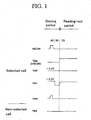
- a series of operations of the MOS image sensor are made to pass through a storing period, a reading-out period and an initializing period as shown in FIG. 8 (b).
- the storing period optically generated holes are generated by light irradiation and then stored in a hole pocket 25.
- an optical signal proportional to the storage amount of the optically generated holes is detected.
- a high reverse voltage is applied to each electrode, i.e. gate, source and drain, and optically generated holes stored in the hole pocket 25 are discharged to perfectly deplete a hole storage region.
- a potential of a gate electrode (Vpg (VSCAN)) is set to be a low voltage, that is, a ground potential in general, and a drain potential (Vpd) and a source potential (Vps) are set to be higher than the gate potential, that is, about 3.3 V in many cases.
- Vpg VSCAN
- Vpd drain potential
- Vps source potential
- a depletion n-channel MOSFET for optical signal detection is made to maintain a cutoff state (depletion state) in the above-described manner, and then optically generated charges generated in a photo diode are transferred to the carrier pocket 25 under the channel region.
- carriers of the same type as the optically generated charges may be sometimes discharged from levels on an interface between a gate insulating film and the channel region.
- the carriers discharged from the interface levels flow into the carrier pocket 25 to be a leak current. Therefore, holes other than the optically generated charges are stored in the carrier pocket 25.
- optically generated charges which are not generated by a leak current, are normally stored in the carrier pocket 25, there may be some cases where excessive optically generated charges than necessary are stored therein.
- the source potential is lowered, and a margin of the selection and discrimination is reduced, thus causing worsening of a so-called smear characteristic, that is, generation of a bright band with striped-shape in a perpendicular direction on the image screen.
- the object of the present invention is to provide a method of storing optically generated charges by an optical signal in a solid state imaging device, which is capable of preventing generation of a so-called white scratch caused by a leak current due to a discharge of electrons from interface levels between a gate insulating film and a channel region, and of preventing generation of a smear caused by excessively stored optically generated charges.
- the present invention is directed to the method of storing optically generated charges by an optical signal in a solid state imaging device as defined in claim 1.
- a basic constitution of the solid state imaging device for use in the method of storing optically generated charges by an optical signal comprises a unit pixel including a photo diode and an insulated gate field effect transistor for optical signal detection (hereinafter, the insulated gate field effect transistor is referred to as a MOS transistor for optical signal detection or simply as a MOSFET, and in some cases, a term “depletion" may be added to the heads of these abbreviations.) placed adjacently to the photo diode, in which, in the unit pixel, the photo diode and the MOSFET are formed respectively in well regions and connected to each other, and an impurity region of the photo diode and a drain region of the MOSFET are connected to each other, and the carrier pocket storing the optically generated charges is provided in the well region in a peripheral portion of a source region of the MOSFET.
- the optically generated charges generated by light irradiation in the photo diode are transferred to the carrier pocket.
- the channel region of the depletion MOSFET is filled with movable carriers of the same conductivity type as that of the source region (set in an accumulation state), and while preventing a discharge of free charge carrier from interface levels on the channel region, the optically generated charges are transferred to the carrier pocket.
- the channel region is set in a depletion state, a stronger electric field than enough strength to direct the optically generated charges from the photo diode 111 to the carrier pocket is formed to further transfer the remaining optically generated charges to the carrier pocket and make them store therein.
- a gate electrode is held at a positive potential (for example, 2.0 V), and the source region and the drain region is held at a positive potential lower than the positive potential of the gate electrode (for example, 1.6 V).
- a positive potential for example, 2.0 V
- the source region and the drain region is held at a positive potential lower than the positive potential of the gate electrode (for example, 1.6 V).
- the potentials of the drain region and the source region are changed.
- Such applied potentials to the electrode and the regions raises a potential on the surface of the well region, thus a potential difference between a bottom of the potential of the carrier pocket and a top thereof can be set lower.
- the potential of the carrier pocket is set at an appropriate height while the channel region is maintained in the accumulation state. Therefore, during the foregoing period A, the excessive optically generated charges are made to overflow the carrier pocket, and an amount of the optically generated charges stored in the carrier pocket is appropriately maintained, thus preventing a so-called smear.
- the gate electrode is held at a positive voltage (0 V) that is lower than the positive potential of the gate electrode during the period A, and the drain region is held at a positive voltage (for example, 3.3 V) that is higher than the positive potential of the drain region.
- the channel region can be set in a depletion state, a stronger electric field than an enough electric field to move the optically generated charges from a light receiving portion to the carrier pocket can be formed in the well regions, and the remaining optically generated charges can be stored in the carrier pocket without any leavings.
- the photo diode is formed in the well region which serves as a charge generation region generating optically generated charges and as a charge transfer region to the carrier pocket.
- the impurity region of the second conductivity type is formed on the well region of the first conductivity type and thus the photo diode has a so-called buried structure to the optically generated charges.
- the buried structure is defined as a structure such that the well region is not apparent on a surface of a semiconductor substrate. Such buried structure results in preventing the optically generated charges in the photo diode from being captured into interface levels on the channel region. Or it results in suppressing a discharge of charges other than the optically generated charges out of the interface levels on the channel region.
- the field effect transistor for optical signal detection has a drain region extending on the well region from the impurity region and being formed as one body with the impurity region.
- the optically generated charges in the photo diode are prevented from being captured into surface levels on the channel region, or charges other than the optically generated charges are prevented from being discharged out of the interface levels on the channel region and from being stored in the carrier pocket.
- movable charges of the second conductivity type may be accumulated in a surface layer over the entire well regions.
- the optically generated charges in the photo diode are more perfectly prevented from being captured in the interface levels over the entire well regions including the charge generation region, the charge transfer region and the other region, or charges other than the optically generated charges are more perfectly prevented from being discharged out of the interface levels over the entire well regions.
- the carrier pocket becomes an electron pocket (carrier pocket), and stores the optically generated charges.
- the depletion p-channel MOSFET depletion pMOSFET
- sufficient charges holes are induced and accumulated into the channel region, the discharge of the charges (electrons) trapped on the interface levels on the channel region is prevented, and the potential in the carrier pocket is set at an appropriate height.
- FIG. 1 is a timing chart showing a method of storing optically generated charges by an optical signal in a solid state imaging device in the conventional example.
- FIG. 2 is a timing chart showing a method of storing optically generated charges by an optical signal in a solid state imaging device according to an embodiment of the present invention.
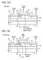
- FIG. 3A is a cross-sectional view showing a state of a peripheral portion of a channel region during a period A of a storing period in the method of storing optically generated charges by an optical signal in FIG. 2A.
- FIG. 3B is a cross sectional view showing a state of a peripheral portion of a channel region during a period A0 of a storing period in the method of storing optically generated charges by an optical signal in FIG. 1, the cross sectional view according to a comparative example.
- FIG. 4A is a graph showing a state of a change in an energy band of a depth direction, the graph corresponding to FIG. 3A.
- FIG. 4B is a graph showing a state of a change in an energy band of a depth direction, the graph corresponding to FIG. 3B.
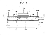
- FIG. 5 is an element cross-sectional view of a MOSFET for optical signal detection, which explains the method of storing optically generated charges by an optical signal in a solid state imaging device according to the embodiment of the present invention.
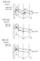
- FIGs. 6A to 6C are views respectively showing states of changes in the energy band in a lateral direction (direction along a line III-III of FIG. 5) from a well region under a drain region through a well region under a channel region including a carrier pocket to a well region under a source region during a period A of a storing period, a period B and a reading-out period (period C).
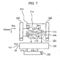
- FIG. 7 is a view showing a circuit constitution of an entire solid state imaging device for use in the method of storing optically generated charges by an optical signal in a solid state imaging device according to the embodiment of the present invention.
- FIG. 8 is a cross-sectional view showing a solid state imaging device for use in the method of storing optically generated charges by an optical signal according to the embodiment of the present invention.
- FIG. 8 is a cross-sectional view of an element in the unit pixel of the MOS image sensor.
- a photo diode 111 and a MOSFET 112 for optical signal detection are provided adjacently to each other.
- a depletion n-channel MOSFET (depletion nMOSFET) is employed.
- the cross-sectional constitution of this unit pixel 101 is, sequentially from the lower, a p-type substrate 11, an n-type epitaxial layer 12 formed on the substrate 11, and first and second p-type well regions 15a and 15b formed in the epitaxial layer 12.
- the photo diode 111 and the MOSFET 112 are respectively formed in the a first and a second well regions 15a and 15b, and the first and second well regions 15a and 15b are connected to each other.
- the first well region 15a of the photo diode 111 constitutes a part of a charge generation region by light irradiation.
- the second well region 15b of the MOSFET 112 constitutes a gate region capable of changing a threshold voltage of a channel by a potential applied to the second well region 15b.
- the first well region 15a and the epitaxial layer 12 are connected to the gate region 15b of the MOSFET 112, holes among charges generated by lights can be used effectively as charges for threshold voltage modulation of the MOSFET 112. In other words, the first well region 15a and the epitaxial layer 12 become entirely the carrier generation region.
- the gate electrode 19 is ring-shaped.
- a source region 16 is formed so as to be surrounded with the inner periphery of the ring-shaped gate electrode 19, while a drain region 17a is formed so as to surround the outer peripheral portion of the ring-shaped gate electrode 19.
- the drain region 17a is extended to form an n-type impurity region 17 of the photo diode 111.
- the impurity region 17 and the drain region 17a are integrally formed with each other such that most regions thereof can be placed in contact with surface layers of the first and second well regions 15a and 15b.
- a surface layer of the second well region 15b between the drain region 17a and the source region 16 becomes an n-channel region (hereinafter, simply referred to as a channel region in some cases). Further, in order to maintain the channel region in an electron storing or depletion state at a usual operation voltage, n-type impurities having a proper density are introduced to the channel region to form a channel doped layer 15c.
- the gate electrode 19 is formed on the channel region by interpolating a gate insulating film 18.
- a p+-type carrier pocket (high-density buried layer) 25 is formed in a part of the region in the channel-length direction in the second well region 15b below the n-channel region, and across the entire region in the channel-width direction, i.e., in the peripheral portion of the source region 16 so as to surround the source region 16.
- the carrier pocket 25 is formed in the second well region 15b under the channel region.
- An impurity density of the foregoing p+-type carrier pocket 25 is set higher than that of the well regions 15a and 15b in the peripheral portion of the carrier pocket. Therefore, a potential in the carrier pocket 25 is lower than a potential in the peripheral portion of the carrier pocket 25 for optically generated holes among optically generated charges. Accordingly, the optically generated holes can be collected in the carrier pocket 25.
- the solid state imaging device applying the present invention has a buried structure to the optically generated charges over the entire well regions 15a and 15b including the charge-generating region, the charge-transferring region and the charge-storage region and the other region except for the channel dope layer 15c.
- the optically generated charges as described above are more perfectly prevented from being captured in the surface levels, or charges other than the optically generated charges are more perfectly prevented from being discharged out of the surface levels and from being stored in the carrier pocket 25 by forming the accumulation state of electrons over a resultant entire surface layer of the well regions 15a and 15b through transforming the channel dope layer 15c to an accumulation state of electrons upon applying a voltage to the gate electrode 19 and so on.
- a so-called buried layer may be formed at least in the photo diode 111 when occasion demands.
- FIG. 7 shows a circuit constitution of the MOS image sensor according to the embodiment of the present invention.
- this MOS image sensor employs the constitution of a two-dimensional array sensor, and the unit pixels 101 structured in the foregoing manner are arrayed in row and column directions in a matrix shape.
- a driving scanning circuit 102 for a vertical scanning signal (VSCAN) and a driving scanning circuit 103 for a drain voltage (VDD) are arranged right and left sandwiching a pixel region.
- Vertical scanning signal supply lines 21a and 21b are drawn out, one for each row, from the driving scanning circuit 102 for the vertical scanning signal (VSCAN).
- the vertical scanning signal supply lines 21a and 21b are connected to the gate electrode 19 of the MOSFET 112 in each of all the pixels 101 arrayed in the row direction.
- Drain voltage supply lines (VDD supply lines) 22a and 22b are drawn out, one for each row, from the driving scanning circuit 103 for the drain voltage (VDD). Each of the drain voltage supply lines (VDD supply lines) 22a and 22b is connected to the drain region 17a of the MOSFET 112 for optical signal detection in each of all the pixels 101 arrayed in the row direction.
- Vertical output lines 20a and 20b different for each column are provided. Each of these vertical output lines 20a and 20b is connected to the source region 16 of the MOSFET 112 in each of all the pixels 101 arrayed in the column direction.
- the source region 16 of the MOSFET 112 is connected, for each column, to a signal output circuit 105 through the vertical output lines 20a and 20b.
- the signal output circuit 105 stores a potential of the source region 16, and further, outputs a video signal corresponding to the potential of the source region 16 through a horizontal output line 26 to a video signal output terminal 107.
- An HSCAN input scanning circuit 104 controls a timing of the output.
- FIG. 2 shows a timing chart of the input/output signals for operating the MOS image sensor according to the present invention.
- the photodetecting operation is carried out by repeating, as described above, a series of periods including storing, reading-out, and sweeping (initializing).
- the storing period is a period for storing the optically generated charges generated by light irradiation in the carrier pocket 25.
- the reading-out period is a period for reading out modulation of the threshold voltage corresponding to the optically generated charges stored in the carrier pocket 25.
- the initializing period is a period for discharging the optically generated charges remaining in the carrier pocket 25.
- the period B among the storing period is a period for terminating the storing period, the period B following the period A.
- FIG. 3A is a cross-sectional view showing a state of the channel region of the MOSFET portion and a peripheral portion thereof during the period A of FIG. 2 according to the present invention.
- FIG. 4A is a diagram showing a state of a change in an energy band of a depth direction along a line I-I of FIG. 3A.
- an energy level at the upper portion indicates a bottom of a conduction band
- an energy level at the lower portion indicates a top of a valence band.
- FIG. 5 is an element cross-sectional view showing a state of the channel region of the MOSFET 112 portion and a peripheral portion thereof during the period B of FIG. 2.
- FIGs. 6A to 6C are views respectively showing states of changes in the energy band in a lateral direction (direction along the line III-III of FIG. 5) from the well region 15b under the drain region 17a through the well region 15b under the channel region including the carrier pocket 25 to the well region 15b under the source region 16 during the period A, the period B and the period C.
- the energy level at the upper portion indicates a bottom of a conduction band
- the energy level at the lower portion indicates a top of a valence band.
- the gate electrode 19 of the MOSFET 112 for optical signal detection is held at a positive potential, for example, +2.3 to 2.5 V, which is equal to a positive potential of the gate electrode 19 during the reading-out period C (hereinafter, sometimes referred to as a gate potential).
- the drain region 17a is held at a positive potential, for example, +1.6 V, such that a pn junction formed of the drain region 17a, the source region 16 and the well region 15b is reversely biased, the channel region is not depleted for the gate potential of + 2.3 to 2.5 V, and electrons are accumulated with a sufficient density in the channel region.
- the source region 16 of the MOSFET 112 is isolated from an outside circuit such that a current does not flow through the channel region of the MOSFET 112.
- This potential holding is carried out for the entire pixels irrespective of the selected rows for reading-out or the non-selected rows therefor.
- electrons of a sufficient density are accumulated in the channel region.
- electrons accumulated in the channel region is to be supplied from the source region 16 and the drain region 17a.
- the source region 16 is connected to the drain region 17a through the channel region, and is held at a positive potential of about + 1.6 V (VDD) equal to the positive potential in the drain region 17a.
- VDD + 1.6 V
- the photo diode 111 is irradiated with lights to generate an electron and hole pair (optically generated charges).
- the optically generated holes among the optically generated charges are stored in the first well region 15a of the photo diode 111.
- the potential in the carrier pocket 25 for the holes is lower than the potential in the first and second well regions 15a and 15b in the peripheral portion. Accordingly, as shown in FIG. 6A, the optically generated holes stored in the first well region 15a are moved to the carrier pocket 25 and stored therein.
- the channel region is set in an accumulation state to store a sufficient amount of electrons.
- hole generating centers on the interface levels between the gate insulating film 18 and the channel region are maintained in a non-active state, and the discharge of the holes is prevented.
- the storage of the holes other than the optically generated charges in the carrier pocket 25 is suppressed, thus the occurrence of a so-called white scratch on the image screen can be prevented.
- the potential of the gate electrode 19 is held at 2.5 V and the potentials of the drain region 17a and the source region 16 are respectively held at 1.6 V such that the channel region is maintained in the accumulation state, as shown in FIG. 4A, the energy level on the surface of the p-type well region 15b is pushed down (the potential is raised), thus a difference of the energy levels (potentials) between the bottom of the carrier pocket 25 and the top thereof is reduced.
- the potentials of the gate electrode 19, the drain region 17a and the source region 16 are appropriately adjusted, thus the difference of the energy levels (potentials) in the carrier pocket 25 can be set at an appropriate height while the channel region is maintained in the accumulation state. Therefore, the amount of the optically generated holes stored in the carrier pocket 25 is appropriately maintained.
- the output (Vpg) of the VSCAN driving scanning circuit 102 is maintained at a ground potential (which becomes the gate potential of the MOSFET 112).
- the potentials of the VDD driving scanning lines 22a and 22b are maintained at a voltage of about 3.3 V (which becomes the drain potential of the MOSFET 112) such that the pn junctions formed between the drain region 17a and the well region 15b, and between the source region 16 and the well region 15b are reversely biased more deeply than that is biased during the period A.
- This potential holding is also carried out for all the pixels irrespective of the selected rows for reading-out or the non-selected rows therefor.
- the channel region is maintained in the depletion state, and a stronger electric field going toward the carrier pocket 25 is generated in the well region 15b.
- the entire optically generated charges remaining in the well regions 15a and 15b are transferred to the carrier pocket 25 to be stored therein.
- a negative charge amount of the acceptor which corresponds to the charge amount of the stored optically generated charges, are neutralized.
- the potential of the charges in the vicinity of the source region 16 is modulated to change the threshold voltage of the depletion nMOSFET 112.
- the operation transfers to the reading-out period (period C).
- the potentials of the VDD driving scanning lines 22a and 22b are entirely kept to be held at a voltage of about 3.3 V (which becomes the drain potential of the MOSFET 112).
- a voltage of about 3.3 V which becomes the drain potential of the MOSFET 1112.
- the output (Vpg) of the VSCAN driving scanning circuit 102 which corresponds to the selected rows for reading-out, is set at a voltage of about 2.3 to 2.5 V (which becomes the gate potential of the MOSFET 112), and the output (Vpg) of the VSCAN driving scanning circuit 102, which corresponds to the non-selected rows for reading-out, is set at a ground potential.
- the potential of the gate electrode 19 is held at a voltage of about 2 to 3 V and the potential of the drain region 17a is held at a VDD potential of about 3.3 V such that the MOSFETs 112 arrayed in the selected rows for reading-out can be operated in a saturated state. Therefore, a high electric field region is formed in the channel region close to the drain region 17a, and an accumulation region of a low electric field is formed in a part of the channel region above the carrier pocket 25 close to the source region 16.
- the source potentials corresponding to the modulation of the threshold voltage due to the optically generated charges are sequentially stored in the memories of the signal output circuit 105, which are connected to the source regions 16 of the MOSFETs 112 arrayed in the selected rows for reading-out.
- the operation returns to the storing period through the initializing operation.
- the output timing is controlled according to the signal inputted to the signal output circuit 105 from the HSCAN input scanning circuit 104.
- the video signal (Vout) proportional to the amount of irradiated light, which is stored in the signal output circuit 105 during the previous period, can be sequentially taken out.
- the optically generated holes are transferred to the carrier pocket 25 to be stored therein, while movable electrons are accumulated in the channel region of the MOSFET 112 for optical signal detection to maintain the channel region in the accumulation state so that the discharge of the holes trapped on the interface levels is prevented.
- the amount of the optically generated holes stored in the carrier pocket 25 can be held appropriately, a so-called smear on the video screen can be prevented.
- FIG. 3B is a cross-sectional view showing a state of the channel region of the MOSFET and a peripheral portion thereof during a storing period A0 of FIG. 1 according to the comparative example.
- FIG. 4B is a view showing a state of a change in an energy band of a depth direction along a line II-II.
- the gate potential is a ground potential during the storing period A0, and is lower than the source potential and the drain potential, the channel region comes in a depletion state. Accordingly, since the interface levels in the channel region are covered with a depletion layer, there is a fear that the trapped holes are discharged from the interface level and the discharged holes are stored in the carrier pocket 25. In addition, there is a fear that the optically generated holes during the transfer into the carrier pocket 25 are trapped onto the interface levels. Therefore, there comes a fear that the optical signal detection cannot be performed with high precision.
- the potentials are held in the drain region 17a and the source region 16 such that, particularly, the pn junctions formed between the drain region 17a and the well region 15b, and between the source region 16 and the well region 15b are reversely biased.
- the drain region 17a and the source region 16 may be held at a ground potential to make the foregoing pn junction zero-bias.
- the photo diode 111 and the MOSFET 112 for optical signal detection may constitute the unit pixel while being adjacent to each other, and that the carrier pocket (high-density buried layer) 25 may be provided in the vicinity of the source region 16 within the p-type well region 15b under the channel region of the MOSFET 112.
- the p-type substrate 11 is used, but instead, an n-type substrate may be used.
- an n-type substrate may be used.
- the well regions and the carrier pocket are of an n-type
- the carrier pocket becomes an electron pocket
- the carriers to be stored in the carrier pocket are electrons between the two, which are electrons and holes.
- p-type impurities are introduced to the channel region (p-channel region) to form a channel doped layer, and during the transfer or storage of the optically generated charges into the carrier pocket, sufficient charges of a conductivity type reverse to that of the well region, that is, sufficient holes are stored in the channel doped layer.
- the potentials of the gate electrode, the drain region and the source region are held such that the channel region is maintained to be in a state where the movable holes are accumulated, a potential difference between a bottom of the potential of the carrier pocket and a top thereof is lowered. Accordingly, the potentials of the gate electrode, the drain region and the source region are adjusted to maintain the channel region in the accumulation state, and the potential of the carrier pocket is set so as to have an appropriate height, thus the amount of the optically generated electrons stored in the carrier pocket can be held appropriately. Therefore, a so-called smear on the video screen can be prevented.
- the channel region is set in an accumulation state at least during the transfer of the optically generated charges such that the optically generated charges transferred from the photo diode to the carrier pocket and stored therein are not affected by the charges trapped on the interface levels in the channel region.
- the channel region is maintained in the accumulation state, thus the charge generating centers on the interface levels in the channel region are maintained in a non-active state, and the discharge of the charges from the interface levels is prevented.
- the leak current is suppressed, the storage of the charges other than the optically generated charges into the carrier pocket is suppressed, thus the occurrence of a so-called white scratch on the video screen can be prevented.
- an accumulation state of electrons may be formed in a surface layer over the entire well region by forming at least the photo diode of a buried structure.
- the difference of the potentials between the bottom of the carrier pocket and the top thereof can be set so as to have an appropriate height, thus the amount of the optically generated charges stored in the carrier pocket can be appropriately held to prevent a so-called smear on the video screen.
Landscapes
- Engineering & Computer Science (AREA)
- Multimedia (AREA)
- Signal Processing (AREA)
- Solid State Image Pick-Up Elements (AREA)
- Transforming Light Signals Into Electric Signals (AREA)
Claims (8)
- Verfahren zur Speicherung optisch erzeugter erregter Ladungen durch ein optisches Signal in einer Festkörperbildsensoreinrichtung mit einer Pixeleinheit (101), diea) eine Fotodiode (111), die versehen ist mita1) einer Halbleiterschicht (15a, 15b) eines ersten Leitfähigkeitstyps, und a2) einem Verunreinigungsbereich (17) eines zweiten Leitfähigkeitstyps, der auf einer Oberflächenschicht der Halbleiterschicht (15a, 15b) so ausgebildet ist, dass die Fotodiode (111) eine vergrabene bzw. verborgene Struktur hat, undb) einen Feldeffekttransistor (112) für die optische Signalerkennung enthält, der in der Nähe der Fotodiode (111) angeordnet und versehen ist mitwobei das Verfahren die folgenden Schritte aufweist:b1) einem Source- bzw. Quellenbereich (16) eines zweiten Leitfähigkeitstyps, der auf der Halbleiterschicht (15a, 15b) ausgebildet ist,b2) einem Drain- bzw. Senkenbereich (17a) des zweiten Leitfähigkeitstyps, der auf der Halbleiterschicht (15a, 15b) ausgebildet und mit dem Verunreinigungsbereich (17) verbunden ist,b3) einem Kanal- bzw. Channelbereich (15c), der auf einer Oberflächenschicht der Halbleiterschicht (15a, 15b) zwischen dem Quellenbereich (16) und dem Senkenbereich (17a) ausgebildet ist,b4) eine Steuer- bzw. Gatelektrode (19), die durch Interpolieren eines gateisolierenden Films (18) den gesamten Kanalbereich (15c) bedeckt, undb5) einer hochdichten, vergrabenen Schicht (25) des ersten Leitfähigkeitstyps, die in der Halbleiterschicht (15a, 15b) unter dem Kanalbereich (15c) vorgesehen ist;i) Erzeugen von optischen Ladungen in der Fotodiode (111) durch Lichtbestrahlung;ii) Überführen der optisch erzeugten Ladungen zu der hochdichten vergrabenen Schicht (25), während bewegliche Ladungen des zweiten Leitfähigkeitstyps über dem gesamten Kanalbereich (15c) beim Halten des Potentials der Steuerelektrode (19) angesammelt werden, undiii) Speichern der optisch erzeugten Ladungen des ersten Leitfähigkeitstyps in der hochdichten vergrabenen Schicht (25), während bewegliche Ladungen des zweiten Leitfähigkeitstyps über dem gesamten Kanalbereich (15c) beim Halten des Potentials der Steuerelektrode (19) angesammelt werden.
- Verfahren zum Speichern von optisch erzeugten Ladungen durch ein optisches Signal in einer Festkörperbildsensoreinrichtung nach Anspruch 1, wobei bewegliche Ladungen des gleichen Leitfähigkeitstyps wie der des Quellenbereichs (16) über der gesamten Oberflächenschicht der Halbleiterschicht (15a, 15b) einschließlich des Kanalbereichs (15c) wenigstens bei den Schritten der Überführung und Speicherung angesammelt werden.
- Verfahren zum Speichern von optisch erzeugten Ladungen durch ein optisches Signal in einer Festkörperbildsensoreinrichtung nach Anspruch 1, wobei die Halbleiterschicht (15a, 15b) aus einer ersten Halbleiterschicht (15a) und einer zweiten Halbleiterschicht (15b) zusammengesetzt ist, die miteinander verbunden sind, der Verunreinigungsbereich auf der ersten Halbleiterschicht (15a) ausgebildet ist, der Quellenbereich und der Senkenbereich (17a) auf der Halbleiterschicht (15b) ausgebildet sind, der Kanalbereich (15c), auf dem eine kanaldotierte Schicht ausgebildet ist, auf einer Oberflächenschicht der zweiten Halbleiterschicht (15b) ausgebildet ist und die hochdichte vergrabene Schicht (25) in der zweiten Halbleiterschicht (15b) vorgesehen wird.
- Verfahren zur Speicherung von optisch erzeugten Ladungen durch ein optisches Signal in einer Festkörperbildsensoreinrichtung nach Anspruch 1 oder Anspruch 3, wobei der Feldeffekttransistor (112) für die optische Signalerkennung vom Verarmungstyp ist.
- Verfahren zur Speicherung von optisch erzeugten Ladungen durch ein optisches Signal in einer Festkörperbildsensoreinrichtung nach Anspruch 3, wobei bewegliche Ladungen des zweiten Leitfähigkeitstyps über der gesamten Oberflächenschicht der ersten und zweiten Halbleiterschciht (15a, 15b) einschließlich des Kanalbereichs (15c) wenigstens bei den Schritten der Überführung und Speicherung angesammelt werden.
- Verfahren zur Speicherung von optisch erzeugten Ladungen durch ein optisches Signal in einer Festkörperbildsensoreinrichtung nach Anspruch 1 oder 3, wobei ein Strom zu dem Feldeffekttransistor (112) für die optische Signalerkennung fließt, um eine Änderung in dem Schwellenwert nach einer Periode auszulesen, wenn die optisch erzeugten Ladungen zu der hochdichten vergrabenen Schicht (25) übertragen werden, um darin gespeichert zu werden.
- Verfahren zur Speicherung von optisch erzeugten Ladungen durch ein optisches Signal in einer Festkörperbildsensoreinrichtung nach Anspruch 3, weiterhin mit einer Vielzahl von Pixeln (101), die in Reihen und Spalten angeordnet sind, wobei die optischen Signale in den jeweiligen Pixeln durch Zuführung unterschiedlicher Abtastsignale zu den wechselseitig angeschlossenen Steuerelektroden (19) des Feldeffekttransistors (112), die in der gleichen Reihe angeordnet sind, dem wechselseitig verbundenen Senkenbereich (17a) des Feldeffekttransistors (112), der in der gleichen Reihe angeordnet ist, und dem wechselseitig verbundene Quellenbereich (16) des Feldeffekttransistors (112), der in der gleichen Spalte angeordnet ist, gespeichert werden.
- Verfahren zur Speicherung von optisch erzeugten Ladungen durch ein optisches Signal in einer Festkörperbildsensoreinrichtung nach Anspruch 7, wobei des Speichern der optischen Signale in den jeweiligen Pixeln (101) und das Auslesen der gespeicherten optischen Signale durch ein vertikales Abtastsignal, das eine Abtastschaltung (102) für die Zuführung eines Abtastsignals zu der Steuerelektrode (19) in der Reihe treibt, eine Senkenspannungs-Treiberabtastschaltung (103) für die Zuführung einer Senkenspannung zu dem Senkenbereich (17a) in der Reihe, eine Signalausgabeschaltung (105) für die Speicherung der Spannungen der Quellenbereiche (16) in der Spalte und weiterhin für die Ausgabe eines optischen Signals, das der Spannung jedes Quellenbereichs (16) entspricht, und eine Abtastschaltung (104) für ein horizontales Abtasteingangssignal für die Zuführung eines Abtastsignals zur Steuerung des Zeitablaufs des Auslesens des optischen Signals. gesteuert werden,
Applications Claiming Priority (8)
| Application Number | Priority Date | Filing Date | Title |
|---|---|---|---|
| JP2000044886 | 2000-02-22 | ||
| JP2000044886 | 2000-02-22 | ||
| JP2000237521 | 2000-08-04 | ||
| JP2000237521 | 2000-08-04 | ||
| JP2000246416 | 2000-08-15 | ||
| JP2000246416 | 2000-08-15 | ||
| JP2000292786 | 2000-09-26 | ||
| JP2000292786 | 2000-09-26 |
Publications (3)
| Publication Number | Publication Date |
|---|---|
| EP1128437A2 EP1128437A2 (de) | 2001-08-29 |
| EP1128437A3 EP1128437A3 (de) | 2002-11-27 |
| EP1128437B1 true EP1128437B1 (de) | 2008-01-02 |
Family
ID=27481058
Family Applications (1)
| Application Number | Title | Priority Date | Filing Date |
|---|---|---|---|
| EP01102805A Expired - Lifetime EP1128437B1 (de) | 2000-02-22 | 2001-02-09 | Verfahren zur Speicherung optisch erregter Ladungen in einer Festkörperbildsensoreinrichtung |
Country Status (5)
| Country | Link |
|---|---|
| US (1) | US6950134B2 (de) |
| EP (1) | EP1128437B1 (de) |
| KR (1) | KR100377599B1 (de) |
| CN (1) | CN1162915C (de) |
| DE (1) | DE60132122T2 (de) |
Families Citing this family (16)
| Publication number | Priority date | Publication date | Assignee | Title |
|---|---|---|---|---|
| JP4109858B2 (ja) * | 2001-11-13 | 2008-07-02 | 株式会社東芝 | 固体撮像装置 |
| US6921934B2 (en) * | 2003-03-28 | 2005-07-26 | Micron Technology, Inc. | Double pinned photodiode for CMOS APS and method of formation |
| JP4004484B2 (ja) * | 2004-03-31 | 2007-11-07 | シャープ株式会社 | 固体撮像素子の製造方法 |
| KR100658615B1 (ko) * | 2004-04-29 | 2006-12-15 | 삼성에스디아이 주식회사 | 발광 표시 패널 및 발광 표시 장치 |
| FR2884351A1 (fr) * | 2005-04-11 | 2006-10-13 | St Microelectronics Sa | Procede de fabrication d'un circuit integre comprenant une photodiode et circuit integre correspondant. |
| JP2006294871A (ja) * | 2005-04-11 | 2006-10-26 | Matsushita Electric Ind Co Ltd | 固体撮像装置 |
| EP1722421A3 (de) * | 2005-05-13 | 2007-04-18 | Stmicroelectronics Sa | Integrierte massefreie Fotodiode |
| EP1722422A3 (de) * | 2005-05-13 | 2007-04-18 | Stmicroelectronics Sa | Integrierter Schaltkreis mit einer massefreien Fotodiode und Herstellungsverfahren dafür |
| US7875916B2 (en) * | 2005-09-28 | 2011-01-25 | Eastman Kodak Company | Photodetector and n-layer structure for improved collection efficiency |
| US7728277B2 (en) | 2005-11-16 | 2010-06-01 | Eastman Kodak Company | PMOS pixel structure with low cross talk for active pixel image sensors |
| US20080138926A1 (en) | 2006-12-11 | 2008-06-12 | Lavine James P | Two epitaxial layers to reduce crosstalk in an image sensor |
| FR2911007B1 (fr) * | 2006-12-28 | 2009-10-02 | St Microelectronics Sa | Capteur d'image comprenant des pixels a un transistor |
| US7804052B2 (en) * | 2007-06-08 | 2010-09-28 | Aptina Imaging Corp. | Methods and apparatuses for pixel testing |
| JP4715931B2 (ja) * | 2009-02-10 | 2011-07-06 | ソニー株式会社 | 電荷検出装置及び電荷検出方法、並びに固体撮像装置及びその駆動方法、並びに撮像装置 |
| JP2010283597A (ja) * | 2009-06-04 | 2010-12-16 | Toshiba Corp | 半導体撮像装置 |
| US20140104942A1 (en) * | 2012-10-12 | 2014-04-17 | Samsung Electronics Co., Ltd. | Recess gate transistors and devices including the same |
Family Cites Families (16)
| Publication number | Priority date | Publication date | Assignee | Title |
|---|---|---|---|---|
| JPS5678364U (de) * | 1979-11-14 | 1981-06-25 | ||
| JPS59196669A (ja) * | 1983-04-22 | 1984-11-08 | Matsushita Electronics Corp | 固体撮像装置 |
| JPS60140752A (ja) | 1983-12-28 | 1985-07-25 | Olympus Optical Co Ltd | 半導体光電変換装置 |
| JPH0666446B2 (ja) | 1984-03-29 | 1994-08-24 | オリンパス光学工業株式会社 | 固体撮像素子 |
| US4901129A (en) | 1987-04-10 | 1990-02-13 | Texas Instruments Incorporated | Bulk charge modulated transistor threshold image sensor elements and method of making |
| JPH02304973A (ja) | 1989-05-19 | 1990-12-18 | Hitachi Ltd | 固体撮像装置 |
| US5317174A (en) | 1993-02-19 | 1994-05-31 | Texas Instruments Incorporated | Bulk charge modulated device photocell |
| JPH0730086A (ja) | 1993-06-24 | 1995-01-31 | Sony Corp | 増幅型固体撮像素子 |
| JPH07161958A (ja) * | 1993-12-09 | 1995-06-23 | Nec Corp | 固体撮像装置 |
| JPH09162380A (ja) * | 1995-10-04 | 1997-06-20 | Sony Corp | 増幅型固体撮像素子及びその製造方法 |
| KR970030867A (ko) * | 1995-11-21 | 1997-06-26 | 김광호 | 전하결합소자형 고체촬상소자 |
| JP2827993B2 (ja) | 1995-12-22 | 1998-11-25 | ソニー株式会社 | 固体撮像素子 |
| KR980012584A (ko) * | 1996-07-16 | 1998-04-30 | 김광호 | 리셋 트랜지스터의 게이트 전위 안정화 장치 |
| JP2935492B2 (ja) | 1997-10-30 | 1999-08-16 | イノビジョン株式会社 | 固体撮像素子及び固体撮像素子による光信号検出方法 |
| US6051857A (en) | 1998-01-07 | 2000-04-18 | Innovision, Inc. | Solid-state imaging device and method of detecting optical signals using the same |
| KR19990084630A (ko) * | 1998-05-08 | 1999-12-06 | 김영환 | 씨모스 이미지 센서 및 그 구동 방법 |
-
2001
- 2001-02-01 US US09/774,667 patent/US6950134B2/en not_active Expired - Lifetime
- 2001-02-09 EP EP01102805A patent/EP1128437B1/de not_active Expired - Lifetime
- 2001-02-09 DE DE60132122T patent/DE60132122T2/de not_active Expired - Lifetime
- 2001-02-20 KR KR10-2001-0008388A patent/KR100377599B1/ko not_active Expired - Fee Related
- 2001-02-22 CN CNB011028912A patent/CN1162915C/zh not_active Expired - Fee Related
Also Published As
| Publication number | Publication date |
|---|---|
| EP1128437A2 (de) | 2001-08-29 |
| US6950134B2 (en) | 2005-09-27 |
| CN1162915C (zh) | 2004-08-18 |
| DE60132122T2 (de) | 2008-12-18 |
| KR100377599B1 (ko) | 2003-03-29 |
| EP1128437A3 (de) | 2002-11-27 |
| US20010015468A1 (en) | 2001-08-23 |
| DE60132122D1 (de) | 2008-02-14 |
| KR20010083192A (ko) | 2001-08-31 |
| CN1310478A (zh) | 2001-08-29 |
Similar Documents
| Publication | Publication Date | Title |
|---|---|---|
| US12133006B2 (en) | Solid-state imaging device and imaging system | |
| US6448596B1 (en) | Solid-state imaging device | |
| EP0978878B1 (de) | Festkörper-Bildaufnahmevorrichtung und Verfahren zum Erfassen eines optischen Signals mit Hilfe einer solchen Vorrichtung | |
| EP1128437B1 (de) | Verfahren zur Speicherung optisch erregter Ladungen in einer Festkörperbildsensoreinrichtung | |
| US8183604B2 (en) | Solid state image pickup device inducing an amplifying MOS transistor having particular conductivity type semiconductor layers, and camera using the same device | |
| US20050116259A1 (en) | Solid-state imaging device and method of driving the same | |
| US8367998B2 (en) | Image sensor having a charge pump circuit and a drive transistor | |
| US6476371B2 (en) | Solid state imaging device and driving method thereof | |
| US7061033B2 (en) | Solid-state imaging device | |
| US6445414B1 (en) | Solid-state image pickup device having vertical overflow drain and resistive gate charge transfer device and method of controlling thereof | |
| US6545331B1 (en) | Solid state imaging device, manufacturing method thereof, and solid state imaging apparatus | |
| JP2002057315A (ja) | 固体撮像装置及びその駆動方法 | |
| JP4907941B2 (ja) | 固体撮像装置およびその駆動方法 | |
| US7067860B2 (en) | Solid-state imaging device | |
| JP3652608B2 (ja) | 固体撮像装置の光信号の蓄積方法 | |
| JP3889389B2 (ja) | 固体撮像装置 | |
| KR100269636B1 (ko) | 고체촬상소자 | |
| US20100060761A1 (en) | Solid-state imaging device and imaging apparatus | |
| JP2005294555A (ja) | 固体撮像素子およびその製造方法、電子情報機器 | |
| JP2005183921A (ja) | 固体撮像装置 | |
| JPS642271B2 (de) | ||
| JP2006032537A (ja) | 固体撮像装置 | |
| JP2006253177A (ja) | 固体撮像装置 |
Legal Events
| Date | Code | Title | Description |
|---|---|---|---|
| PUAI | Public reference made under article 153(3) epc to a published international application that has entered the european phase |
Free format text: ORIGINAL CODE: 0009012 |
|
| AK | Designated contracting states |
Kind code of ref document: A2 Designated state(s): AT BE CH CY DE DK ES FI FR GB GR IE IT LI LU MC NL PT SE TR |
|
| AX | Request for extension of the european patent |
Free format text: AL;LT;LV;MK;RO;SI |
|
| PUAL | Search report despatched |
Free format text: ORIGINAL CODE: 0009013 |
|
| AK | Designated contracting states |
Kind code of ref document: A3 Designated state(s): AT BE CH CY DE DK ES FI FR GB GR IE IT LI LU MC NL PT SE TR |
|
| AX | Request for extension of the european patent |
Free format text: AL;LT;LV;MK;RO;SI |
|
| 17P | Request for examination filed |
Effective date: 20030115 |
|
| AKX | Designation fees paid |
Designated state(s): DE FR GB IT NL |
|
| 17Q | First examination report despatched |
Effective date: 20050607 |
|
| GRAP | Despatch of communication of intention to grant a patent |
Free format text: ORIGINAL CODE: EPIDOSNIGR1 |
|
| GRAS | Grant fee paid |
Free format text: ORIGINAL CODE: EPIDOSNIGR3 |
|
| GRAA | (expected) grant |
Free format text: ORIGINAL CODE: 0009210 |
|
| AK | Designated contracting states |
Kind code of ref document: B1 Designated state(s): DE FR GB IT NL |
|
| REG | Reference to a national code |
Ref country code: GB Ref legal event code: FG4D |
|
| REF | Corresponds to: |
Ref document number: 60132122 Country of ref document: DE Date of ref document: 20080214 Kind code of ref document: P |
|
| PG25 | Lapsed in a contracting state [announced via postgrant information from national office to epo] |
Ref country code: NL Free format text: LAPSE BECAUSE OF FAILURE TO SUBMIT A TRANSLATION OF THE DESCRIPTION OR TO PAY THE FEE WITHIN THE PRESCRIBED TIME-LIMIT Effective date: 20080102 |
|
| NLV1 | Nl: lapsed or annulled due to failure to fulfill the requirements of art. 29p and 29m of the patents act | ||
| ET | Fr: translation filed | ||
| PLBE | No opposition filed within time limit |
Free format text: ORIGINAL CODE: 0009261 |
|
| STAA | Information on the status of an ep patent application or granted ep patent |
Free format text: STATUS: NO OPPOSITION FILED WITHIN TIME LIMIT |
|
| 26N | No opposition filed |
Effective date: 20081003 |
|
| PG25 | Lapsed in a contracting state [announced via postgrant information from national office to epo] |
Ref country code: IT Free format text: LAPSE BECAUSE OF FAILURE TO SUBMIT A TRANSLATION OF THE DESCRIPTION OR TO PAY THE FEE WITHIN THE PRESCRIBED TIME-LIMIT Effective date: 20080102 |
|
| PGFP | Annual fee paid to national office [announced via postgrant information from national office to epo] |
Ref country code: FR Payment date: 20100226 Year of fee payment: 10 |
|
| PGFP | Annual fee paid to national office [announced via postgrant information from national office to epo] |
Ref country code: DE Payment date: 20100219 Year of fee payment: 10 Ref country code: GB Payment date: 20100218 Year of fee payment: 10 |
|
| GBPC | Gb: european patent ceased through non-payment of renewal fee |
Effective date: 20110209 |
|
| REG | Reference to a national code |
Ref country code: FR Ref legal event code: ST Effective date: 20111102 |
|
| REG | Reference to a national code |
Ref country code: DE Ref legal event code: R119 Ref document number: 60132122 Country of ref document: DE Effective date: 20110901 |
|
| PG25 | Lapsed in a contracting state [announced via postgrant information from national office to epo] |
Ref country code: FR Free format text: LAPSE BECAUSE OF NON-PAYMENT OF DUE FEES Effective date: 20110228 |
|
| PG25 | Lapsed in a contracting state [announced via postgrant information from national office to epo] |
Ref country code: GB Free format text: LAPSE BECAUSE OF NON-PAYMENT OF DUE FEES Effective date: 20110209 |
|
| PG25 | Lapsed in a contracting state [announced via postgrant information from national office to epo] |
Ref country code: DE Free format text: LAPSE BECAUSE OF NON-PAYMENT OF DUE FEES Effective date: 20110901 |