EP1128559B1 - Dispositif de génération d'un signal oscillant présentant une relation de phase souhaitée avec un signal d'entrée - Google Patents
Dispositif de génération d'un signal oscillant présentant une relation de phase souhaitée avec un signal d'entrée Download PDFInfo
- Publication number
- EP1128559B1 EP1128559B1 EP01301585A EP01301585A EP1128559B1 EP 1128559 B1 EP1128559 B1 EP 1128559B1 EP 01301585 A EP01301585 A EP 01301585A EP 01301585 A EP01301585 A EP 01301585A EP 1128559 B1 EP1128559 B1 EP 1128559B1
- Authority
- EP
- European Patent Office
- Prior art keywords
- signals
- phase
- ring
- signal
- input
- Prior art date
- Legal status (The legal status is an assumption and is not a legal conclusion. Google has not performed a legal analysis and makes no representation as to the accuracy of the status listed.)
- Expired - Lifetime
Links
- 230000010355 oscillation Effects 0.000 claims abstract description 21
- 230000000644 propagated effect Effects 0.000 claims description 2
- 102100040862 Dual specificity protein kinase CLK1 Human genes 0.000 abstract description 9
- 101000749294 Homo sapiens Dual specificity protein kinase CLK1 Proteins 0.000 abstract description 9
- 102100040844 Dual specificity protein kinase CLK2 Human genes 0.000 abstract description 8
- 101000749291 Homo sapiens Dual specificity protein kinase CLK2 Proteins 0.000 abstract description 8
- 238000011084 recovery Methods 0.000 description 12
- 238000010586 diagram Methods 0.000 description 5
- 230000002441 reversible effect Effects 0.000 description 5
- 230000000630 rising effect Effects 0.000 description 5
- 230000010363 phase shift Effects 0.000 description 4
- 230000005540 biological transmission Effects 0.000 description 2
- 230000007704 transition Effects 0.000 description 2
- 238000006073 displacement reaction Methods 0.000 description 1
- 238000000034 method Methods 0.000 description 1
- 238000005070 sampling Methods 0.000 description 1
- 238000004088 simulation Methods 0.000 description 1
- 230000003068 static effect Effects 0.000 description 1
Images


Classifications
-
- H—ELECTRICITY
- H03—ELECTRONIC CIRCUITRY
- H03L—AUTOMATIC CONTROL, STARTING, SYNCHRONISATION OR STABILISATION OF GENERATORS OF ELECTRONIC OSCILLATIONS OR PULSES
- H03L7/00—Automatic control of frequency or phase; Synchronisation
- H03L7/06—Automatic control of frequency or phase; Synchronisation using a reference signal applied to a frequency- or phase-locked loop
- H03L7/08—Details of the phase-locked loop
- H03L7/085—Details of the phase-locked loop concerning mainly the frequency- or phase-detection arrangement including the filtering or amplification of its output signal
- H03L7/089—Details of the phase-locked loop concerning mainly the frequency- or phase-detection arrangement including the filtering or amplification of its output signal the phase or frequency detector generating up-down pulses
-
- H—ELECTRICITY
- H03—ELECTRONIC CIRCUITRY
- H03L—AUTOMATIC CONTROL, STARTING, SYNCHRONISATION OR STABILISATION OF GENERATORS OF ELECTRONIC OSCILLATIONS OR PULSES
- H03L7/00—Automatic control of frequency or phase; Synchronisation
- H03L7/06—Automatic control of frequency or phase; Synchronisation using a reference signal applied to a frequency- or phase-locked loop
- H03L7/08—Details of the phase-locked loop
- H03L7/099—Details of the phase-locked loop concerning mainly the controlled oscillator of the loop
- H03L7/0995—Details of the phase-locked loop concerning mainly the controlled oscillator of the loop the oscillator comprising a ring oscillator
- H03L7/0998—Details of the phase-locked loop concerning mainly the controlled oscillator of the loop the oscillator comprising a ring oscillator using phase interpolation
Definitions
- the present invention relates to the control of a phase interpolator circuit such as may be used to generate a data recovery clock signal from a pair of reference clocks.
- EP-A-0909035 describes a phase synchronising arrangement, one possible use of which is the generation of a data recovery clock signal from a pair of quadrature related reference clock signals. Reference may be made to that application for a detailed discussion of the principles involved but an outline description is given in the following.
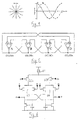
- FIG. 3 A schematic illustration of an implementation of a phase mixer to perform the above mixing is shown in Figure 3.
- each signal is represented by a pair of signal lines.
- the phase mixer comprises four differential amplifiers 31a, 31b, 32a, 32b each of which includes two transistors as illustrated in a conventional fashion.
- Reference clock CLK1 is applied to amplifiers 31a, 31b with opposite polarities, such that one amplifier acts to add the reference clock to the sum signal, while the other subtracts it.
- the current sources I1p, I1n control the extents to which the amplifiers add and subtract the reference signal.
- the current pair I1p, I1n thus are equivalent to the differential circuit weighting W1 enabling W1 to be adjusted from +1 to -1.
- CLK2 is applied to amplifiers 32a, 32b and I2p, I2n are equivalent to W2.
- EP-A-0909035 describes in detail how suitable values of I1p, I1n, I2p, I2n may be generated from a selection of switched current sources of various values. That switching arrangement, and others, however can only provide a certain number of W1, W2 pairs and hence the number of available phase shifts which can be selected is limited. This is illustrated in Figure 4 which corresponds to the arrangement described in EP-A-0909035 and shows a situation where 12 evenly spaced phase shifts are available.
- US patent 5708383 describes a frequency controlled modulator for use in a phase lock loop comprising an adjustable waveform synthesizer.
- the present invention provides apparatus for generating an oscillating signal in a desired phase relationship with an input signal, comprising:
- the present invention provides an arrangement for the generation of the control signals for a phase interpolator, designated I1p, I1n, I2p, I2n above, such that the control signals may be adjusted more finely. More particularly the invention provides signals, the phase of which can be adjusted continuously, or in sufficiently small steps, such that, when input as the control signals to a phase interpolator, fine phase control of the output of the interpolator can be achieved.
- the preferred circuit used to implement the invention is a variation of a ring oscillator circuit, configured such that it provides a pair of signals which correspond to a cos/sin pair, the phase of which can be adjusted to adjust the phase of the interpolator output.
- a phase interpolator is arranged to generate a data recovery clock signal from a pair of quadrature related reference clocks by mixing the reference clocks according to weighting values.
- the frequency of the reference clocks should be close to or the same as the required frequency of the data recovery clock.
- the weighting values are generated by a reversible ring oscillator circuit which outputs a cos/sin pair the phase of which is adjusted by advancing or reversing the ring oscillation according to a phase comparison of the generated data recovery clock and received data.
- EP-A-0828348 describes a phase-tuned ring oscillator in which the frequency of oscillation of the ring can be adjusted.
- the output of each stage in an N stage ring is fed forward M stages as a secondary input to the resulting stage as well as being input as the primary input to the immediately succeeding stage.
- the oscillation frequency can be adjusted by mixing in each stage the primary and secondary inputs in variable proportion.
- the present embodiment is a particular form of that arrangement to generate the weighting values for the phase interpolator.
- N being even means that signals in the required cos/sin relationship are available at opposite points in the ring.
- M being N-2 means that the output of each stage is input to the next stage as the primary input and to the immediately preceding stage as the secondary input.
- FIG. 5 illustrates this in the context of a four stage ring oscillator.
- the signals are shown as single lines, but in the preferred implementation each single line represents a differential pair.
- each single line represents a differential pair.
- the arrangement is symmetrical with regard to the primary (P) inputs and secondary (S) inputs to the stages.
- P primary
- S secondary
- Figure 5 shows a reversible ring oscillator.
- the oscillation proceeds around the ring in the order A ⁇ B ⁇ C ⁇ D
- the S inputs are enabled the oscillation proceeds in the reverse order A ⁇ D ⁇ C ⁇ B.
- effective performance is achieved by using a digital select to enable either the primary inputs or the secondary.
- stage design comprises a current source 61 connected to a pair of PMOS transistors 62a, 62b to which are applied signals D, Dn being a differential pair representing the digital control for the stage.
- the primary input P, Pn is applied to transistor pair 63 controlled by transistor 62a while the secondary input S, Sn is applied to transistor pair 64 controlled by transistor 62b.
- the state of control signal D, Dn will control whether the primary input P, Pn or the secondary input S, Sn is propagated as the output signal O, On, and hence whether the ring oscillates forwards or in reverse as mentioned above.
- the rate at which the phase interpolator is adjusted should be significantly lower than the frequency of the reference clocks.
- the oscillation frequency of the ring oscillator is set lower than the reference clocks and it is designated a Low Frequency Reversible Oscillator (LFRO).
- LFRO Low Frequency Reversible Oscillator
- Control of the phase interpolator is implemented by using outputs from the LFRO as the current weighting values.
- the signals are taken from opposite points in the ring, eg. signals OA, OAn and OC, OCn.
- Phase interpolator 70 of the type shown in detail in Figure 3, generates data recovery clock 30 from reference clocks CLK1, CLK2.
- the control inputs I1p, I1n, I2p, I2n are taken as shown from LFRO 72 which is as shown in Figure 5.
- control of the phase interpolator is effected by the LFRO setting the current weightings.
- the LFRO ring When the LFRO ring is running forward the phase of the interpolator output will advance with respect to the reference clocks, producing an output with frequency f ref + f lfro , where f ref is the frequency of the reference clocks and f lfro is the frequency of the reference oscillator output.
- the ring is reversed the output of the phase interpolator is gradually retarded with reference to the reference clocks, producing an output with frequency f ref - f lfro .
- the generated clock 30 is compared with the received data signal 80. Both signals are applied as shown to a pair of flip-flops 81a, 81b with each data transition being clocked through flip-flop 81a on a rising edge of CLK30 and through flip-flop 81b on a falling edge. Each data transition thus generates a pulse in the output of exclusive-OR gate 32 applied to D inputs of flip-flops 33a, 33b. If a rising edge in received data 80 precedes a rising edge in CLK30, the pulse in the output of gate 32 will begin the rising edge of CLK30 and will accordingly be clocked through flip-flop 33b by the same rising edge as a "pump down" signal. This is applied to Dn in the LFRO to retard the phase of the phase oscillator.
- the normal manner of operation for the LFRO is simply to control the direction of oscillation using a differential logic signal.
- a further feature of the LFRO is the ability to freeze its operation by giving the primary and secondary stages in the ring equal weighting (ie. by setting the oscillation direction control input, D, to zero differential). In reality, this is not a perfect process, and the ring tends to carry on drifting slowly after it has been frozen. However, in practice this is unlikely to be a significant problem in a closed loop clock/data recovery system when the LFRO will be undergoing continual adjustments: the crucial point is that during this mode of operation, the oscillation signals in the ring do not collapse to zero since this would cause the phase interpolator output amplitude to die.
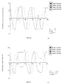
- This operation of the 4-stage LFRO is shown in Figure 10: this is similar to Figure 9 except that the LFRO is held static for a period of 20ns when each change of oscillation direction occurs.
- this arrangement provides a simple configuration enabling close control of the phase of a phase interpolator without the need to provide a large number of different value current sources.
Landscapes
- Stabilization Of Oscillater, Synchronisation, Frequency Synthesizers (AREA)
- Oscillators With Electromechanical Resonators (AREA)
- Networks Using Active Elements (AREA)
Claims (6)
- Dispositif de génération d'un signal oscillant présentant une relation de phase souhaitée avec un signal d'entrée, comprenant :des moyens de mélange (70), agencés pour recevoir une paire de signaux de référence oscillant à une fréquence commune et ayant un déphasage entre eux, et pour mélanger lesdits signaux de référence en des proportions variables selon la valeur de signaux de pondération d'entrée pour générer un signal de sortie ;des moyens de comparaison (74) agencés pour comparer la phase dudit signal de sortie à celle dudit signal d'entrée, afin de déterminer si lesdits signaux sont à ladite relation de phase souhaitée et, dans la négative, pour fournir en sortie un ou plusieurs signaux de commande indicatifs de l'ajustement requis dans la phase dudit signal de sortie pour obtenir ladite relation de phase souhaitée ; et caractérisé parun oscillateur en anneau (72) ajustable comprenant une pluralité d'étages connectés en un anneau et agencés pour propager des oscillations sur ledit anneau, la sortie de chaque étage étant introduite en tant qu'entrée primaire à l'étage suivant dans l'anneau et en tant qu'entrée secondaire à l'étage immédiatement antérieur dans l'anneau, ledit oscillateur en anneau réagissant auxdits un ou plusieurs signaux de commande, pour propager lesdites oscillations, dans une première direction, en activant lesdites entrées primaires et en désactivant lesdites entrées secondaires et, dans une deuxième direction, en désactivant lesdites entrées primaires et en activant lesdites entrées secondaires, et étant agencé pour fournir lesdits signaux de pondération auxdits moyens de mélange, à partir des sorties d'un de ses étages.
- Dispositif selon la revendication 1, dans lequel lesdits signaux de référence sont en relation de quadrature les uns avec les autres, et ledit oscillateur en anneau (72) présente un nombre d'étages pair, de manière que des signaux de pondération, ayant une relation sinus/cosinus mutuelle, soient fournis en des points opposés dans ledit anneau.
- Dispositif selon la revendication 1 ou 2, dans lequel la fréquence de l'oscillation desdits signaux de référence est identique ou similaire à une fréquence d'oscillation escomptée dudit signal d'entrée.
- Dispositif selon l'une quelconque des revendications 1 à 3, dans lequel la fréquence de l'oscillation propagée autour dudit oscillateur en anneau (72) est sensiblement inférieure à la fréquence desdits signaux de référence.
- Dispositif selon l'une quelconque des revendications 1 à 4, dans lequel ledit oscillateur en anneau (72) fournit lesdits signaux de pondération sous la forme de paires de signaux différentiels.
- Dispositif selon la revendication 5, dans lequel lesdits signaux de mélange (70) comprennent une pluralité d'amplificateurs différentiels (31, 32), chaque signal de référence, appliqué à deux desdits amplificateurs différentiels avec une polarité et un courant opposés dans lesdits deux amplificateurs différentiels, étant commandé par la paire différentielle d'un desdits signaux de pondération, la somme des sorties desdits amplificateurs différentiels étant utilisée pour fournir ledit signal de sortie.
Applications Claiming Priority (2)
| Application Number | Priority Date | Filing Date | Title |
|---|---|---|---|
| GB0004298 | 2000-02-23 | ||
| GB0004298A GB2362045B (en) | 2000-02-23 | 2000-02-23 | Analogue-Controlled phase interpolator |
Publications (2)
| Publication Number | Publication Date |
|---|---|
| EP1128559A1 EP1128559A1 (fr) | 2001-08-29 |
| EP1128559B1 true EP1128559B1 (fr) | 2007-05-09 |
Family
ID=9886260
Family Applications (1)
| Application Number | Title | Priority Date | Filing Date |
|---|---|---|---|
| EP01301585A Expired - Lifetime EP1128559B1 (fr) | 2000-02-23 | 2001-02-22 | Dispositif de génération d'un signal oscillant présentant une relation de phase souhaitée avec un signal d'entrée |
Country Status (5)
| Country | Link |
|---|---|
| US (1) | US6466098B2 (fr) |
| EP (1) | EP1128559B1 (fr) |
| AT (1) | ATE362226T1 (fr) |
| DE (1) | DE60128277T2 (fr) |
| GB (1) | GB2362045B (fr) |
Families Citing this family (36)
| Publication number | Priority date | Publication date | Assignee | Title |
|---|---|---|---|---|
| US5978379A (en) | 1997-01-23 | 1999-11-02 | Gadzoox Networks, Inc. | Fiber channel learning bridge, learning half bridge, and protocol |
| US7430171B2 (en) | 1998-11-19 | 2008-09-30 | Broadcom Corporation | Fibre channel arbitrated loop bufferless switch circuitry to increase bandwidth without significant increase in cost |
| WO2001084724A2 (fr) | 2000-04-28 | 2001-11-08 | Broadcom Corporation | Procedes et systemes d'egalisation adaptative pour recepteur |
| JP3636657B2 (ja) * | 2000-12-21 | 2005-04-06 | Necエレクトロニクス株式会社 | クロックアンドデータリカバリ回路とそのクロック制御方法 |
| JP4544780B2 (ja) * | 2001-05-24 | 2010-09-15 | ルネサスエレクトロニクス株式会社 | クロック制御回路 |
| JP4107847B2 (ja) * | 2002-02-01 | 2008-06-25 | 富士通株式会社 | タイミング信号発生回路および受信回路 |
| US8155236B1 (en) | 2002-06-21 | 2012-04-10 | Netlogic Microsystems, Inc. | Methods and apparatus for clock and data recovery using transmission lines |
| TWI289973B (en) * | 2002-10-10 | 2007-11-11 | Via Tech Inc | Method and related circuitry for multiple phase splitting by phase interpolation |
| JP4196657B2 (ja) | 2002-11-29 | 2008-12-17 | 株式会社日立製作所 | データ再生方法およびデジタル制御型クロックデータリカバリ回路 |
| US7151398B2 (en) * | 2003-08-26 | 2006-12-19 | Integrated Device Technology, Inc. | Clock signal generators having programmable full-period clock skew control |
| US6977539B1 (en) | 2003-08-26 | 2005-12-20 | Integrated Device Technology, Inc. | Clock signal generators having programmable full-period clock skew control and methods of generating clock signals having programmable skews |
| US7196562B1 (en) | 2003-08-26 | 2007-03-27 | Integrated Device Technology, Inc. | Programmable clock drivers that support CRC error checking of configuration data during program restore operations |
| US7298194B2 (en) * | 2004-06-12 | 2007-11-20 | Texas Instruments Incorporated | Interpolation |
| KR100630343B1 (ko) | 2004-07-14 | 2006-09-29 | 삼성전자주식회사 | 아날로그 위상 보간 기술을 이용한 클록 데이터 복원 회로및 그 동작 방법 |
| US7532697B1 (en) | 2005-01-27 | 2009-05-12 | Net Logic Microsystems, Inc. | Methods and apparatus for clock and data recovery using a single source |
| KR100679261B1 (ko) | 2005-05-10 | 2007-02-05 | 삼성전자주식회사 | 위상 인터폴레이션 회로 및 그에 따른 위상 인터폴레이션신호의 발생방법 |
| US7321269B2 (en) * | 2005-07-19 | 2008-01-22 | International Business Machines Corporation | High frequency ring oscillator with feed-forward paths |
| US7196564B2 (en) * | 2005-07-22 | 2007-03-27 | Texas Instruments Incorporated | High frequency balanced phase interpolator |
| US7816975B2 (en) | 2005-09-20 | 2010-10-19 | Hewlett-Packard Development Company, L.P. | Circuit and method for bias voltage generation |
| US7769112B2 (en) * | 2005-09-29 | 2010-08-03 | Freescale Semiconductor, Inc. | Method and system for generating wavelets |
| US7432750B1 (en) * | 2005-12-07 | 2008-10-07 | Netlogic Microsystems, Inc. | Methods and apparatus for frequency synthesis with feedback interpolation |
| JP2007180796A (ja) * | 2005-12-27 | 2007-07-12 | Fujitsu Ltd | 差動増幅回路 |
| US7924885B2 (en) * | 2006-11-20 | 2011-04-12 | Siverge Networks Ltd | Methods and apparatuses for circuit emulation multi-channel clock recovery |
| US7777581B2 (en) * | 2007-10-19 | 2010-08-17 | Diablo Technologies Inc. | Voltage Controlled Oscillator (VCO) with a wide tuning range and substantially constant voltage swing over the tuning range |
| US8121239B2 (en) * | 2008-02-11 | 2012-02-21 | Intel Corporation | Unidirectional sweep training for an interconnect |
| US8004335B2 (en) * | 2008-02-11 | 2011-08-23 | International Business Machines Corporation | Phase interpolator system and associated methods |
| US8063683B2 (en) * | 2009-06-08 | 2011-11-22 | Integrated Device Technology, Inc. | Low power clock and data recovery phase interpolator |
| US8520744B2 (en) * | 2010-03-19 | 2013-08-27 | Netlogic Microsystems, Inc. | Multi-value logic signaling in multi-functional circuits |
| US8423814B2 (en) | 2010-03-19 | 2013-04-16 | Netlogic Microsystems, Inc. | Programmable drive strength in memory signaling |
| US8638896B2 (en) * | 2010-03-19 | 2014-01-28 | Netlogic Microsystems, Inc. | Repeate architecture with single clock multiplier unit |
| US8494377B1 (en) | 2010-06-30 | 2013-07-23 | Netlogic Microsystems, Inc. | Systems, circuits and methods for conditioning signals for transmission on a physical medium |
| US8537949B1 (en) | 2010-06-30 | 2013-09-17 | Netlogic Microsystems, Inc. | Systems, circuits and methods for filtering signals to compensate for channel effects |
| US9209821B2 (en) * | 2014-01-24 | 2015-12-08 | Intel Corporation | Apparatus for generating quadrature clock phases from a single-ended odd-stage ring oscillator |
| US20150318860A1 (en) * | 2014-04-30 | 2015-11-05 | Qualcomm Incorporated | Low noise phase locked loops |
| EP3217543B1 (fr) * | 2016-03-11 | 2018-05-09 | Socionext Inc. | Circuit de génération d'horloge |
| CN116846386A (zh) * | 2022-03-23 | 2023-10-03 | 华为技术有限公司 | 鉴频鉴相器、锁相环以及电子设备 |
Family Cites Families (6)
| Publication number | Priority date | Publication date | Assignee | Title |
|---|---|---|---|---|
| US5224125A (en) * | 1991-04-05 | 1993-06-29 | National Semiconductor Corporation | Digital signed phase-to-frequency converter for very high frequency phase locked loops |
| US5132633A (en) * | 1991-05-21 | 1992-07-21 | National Semiconductor Corporation | PLL using a multi-phase frequency correction circuit in place of a VCO |
| US5708383A (en) * | 1996-04-26 | 1998-01-13 | Nat Semiconductor Corp | Integrated circuit frequency controlled modulator for use in a phase lock loop |
| GB9618901D0 (en) * | 1996-09-10 | 1996-10-23 | Phoenix Vlsi Consultants Ltd | Phase-tuned ring oscillator |
| GB9721384D0 (en) * | 1997-10-08 | 1997-12-10 | Phoenix Vlsi Consultants | Phase locked loop |
| DE19949782C1 (de) * | 1999-10-15 | 2001-07-12 | Texas Instruments Deutschland | PLL-Schaltung |
-
2000
- 2000-02-23 GB GB0004298A patent/GB2362045B/en not_active Expired - Lifetime
-
2001
- 2001-02-22 DE DE60128277T patent/DE60128277T2/de not_active Expired - Lifetime
- 2001-02-22 AT AT01301585T patent/ATE362226T1/de not_active IP Right Cessation
- 2001-02-22 EP EP01301585A patent/EP1128559B1/fr not_active Expired - Lifetime
- 2001-02-23 US US09/792,202 patent/US6466098B2/en not_active Expired - Lifetime
Also Published As
| Publication number | Publication date |
|---|---|
| US6466098B2 (en) | 2002-10-15 |
| GB2362045A (en) | 2001-11-07 |
| ATE362226T1 (de) | 2007-06-15 |
| GB2362045B (en) | 2004-05-05 |
| DE60128277D1 (de) | 2007-06-21 |
| EP1128559A1 (fr) | 2001-08-29 |
| US20020125960A1 (en) | 2002-09-12 |
| DE60128277T2 (de) | 2008-01-10 |
| GB0004298D0 (en) | 2000-04-12 |
Similar Documents
| Publication | Publication Date | Title |
|---|---|---|
| EP1128559B1 (fr) | Dispositif de génération d'un signal oscillant présentant une relation de phase souhaitée avec un signal d'entrée | |
| US5451894A (en) | Digital full range rotating phase shifter | |
| US8036300B2 (en) | Dual loop clock recovery circuit | |
| US6242965B1 (en) | Phase synchronization | |
| US5239274A (en) | Voltage-controlled ring oscillator using complementary differential buffers for generating multiple phase signals | |
| US5596610A (en) | Delay stage circuitry for a ring oscillator | |
| US7545188B1 (en) | Multiphase clock generator | |
| US5489864A (en) | Delay interpolation circuitry | |
| US8581651B2 (en) | Duty cycle based phase interpolators and methods for use | |
| EP1538753A1 (fr) | Circuit de combinaison de phase et circuit générateur de signal d'horloge pour transmission de signal à grande vitesse | |
| US5689530A (en) | Data recovery circuit with large retime margin | |
| US6791360B2 (en) | Source synchronous interface using variable digital data delay lines | |
| US8710929B1 (en) | System and method for combined I/Q generation and selective phase interpolation | |
| USRE38482E1 (en) | Delay stage circuitry for a ring oscillator | |
| JP2002141785A (ja) | 位相差信号発生回路並びにこれを用いた多相クロック発生回路及び集積回路 | |
| US5602512A (en) | Comparator of phase between a digital signal and a clock signal, and corresponding phase locked loop | |
| JP4615089B2 (ja) | 遅延ロックループ回路 | |
| WO2023016292A1 (fr) | Système et procédé de récupération d'un signal d'horloge | |
| US6259295B1 (en) | Variable phase shifting clock generator | |
| US20040101079A1 (en) | Delay-lock-loop with improved accuracy and range | |
| JP2001285059A (ja) | リング発振器出力波形間の位相オフセットを補正するための自己補正回路および方法 | |
| EP1158415B1 (fr) | Interface de données parallèles | |
| CN111919387B (zh) | 具有用于相位检测和相位插值的加权输出段的动态加权异或门 | |
| US10659059B2 (en) | Multi-phase clock generation circuit | |
| JP2000124801A (ja) | Pll回路 |
Legal Events
| Date | Code | Title | Description |
|---|---|---|---|
| PUAI | Public reference made under article 153(3) epc to a published international application that has entered the european phase |
Free format text: ORIGINAL CODE: 0009012 |
|
| AK | Designated contracting states |
Kind code of ref document: A1 Designated state(s): AT BE CH CY DE DK ES FI FR GB GR IE IT LI LU MC NL PT SE TR |
|
| AX | Request for extension of the european patent |
Free format text: AL;LT;LV;MK;RO;SI |
|
| 17P | Request for examination filed |
Effective date: 20020228 |
|
| AKX | Designation fees paid |
Free format text: AT BE CH CY DE DK ES LI |
|
| RBV | Designated contracting states (corrected) |
Designated state(s): AT BE CH CY DE DK ES FR GB GR IE IT LI LU MC NL PT SE TR |
|
| RBV | Designated contracting states (corrected) |
Designated state(s): AT BE CH CY DE DK ES FI FR GB GR IE IT LI LU MC NL PT SE TR |
|
| GRAP | Despatch of communication of intention to grant a patent |
Free format text: ORIGINAL CODE: EPIDOSNIGR1 |
|
| GRAS | Grant fee paid |
Free format text: ORIGINAL CODE: EPIDOSNIGR3 |
|
| GRAA | (expected) grant |
Free format text: ORIGINAL CODE: 0009210 |
|
| AK | Designated contracting states |
Kind code of ref document: B1 Designated state(s): AT BE CH CY DE DK ES FI FR GB GR IE IT LI LU MC NL PT SE TR |
|
| PG25 | Lapsed in a contracting state [announced via postgrant information from national office to epo] |
Ref country code: FI Free format text: LAPSE BECAUSE OF FAILURE TO SUBMIT A TRANSLATION OF THE DESCRIPTION OR TO PAY THE FEE WITHIN THE PRESCRIBED TIME-LIMIT Effective date: 20070509 Ref country code: LI Free format text: LAPSE BECAUSE OF FAILURE TO SUBMIT A TRANSLATION OF THE DESCRIPTION OR TO PAY THE FEE WITHIN THE PRESCRIBED TIME-LIMIT Effective date: 20070509 Ref country code: CH Free format text: LAPSE BECAUSE OF FAILURE TO SUBMIT A TRANSLATION OF THE DESCRIPTION OR TO PAY THE FEE WITHIN THE PRESCRIBED TIME-LIMIT Effective date: 20070509 |
|
| REG | Reference to a national code |
Ref country code: GB Ref legal event code: FG4D |
|
| REG | Reference to a national code |
Ref country code: CH Ref legal event code: EP |
|
| REG | Reference to a national code |
Ref country code: IE Ref legal event code: FG4D |
|
| REF | Corresponds to: |
Ref document number: 60128277 Country of ref document: DE Date of ref document: 20070621 Kind code of ref document: P |
|
| PG25 | Lapsed in a contracting state [announced via postgrant information from national office to epo] |
Ref country code: SE Free format text: LAPSE BECAUSE OF FAILURE TO SUBMIT A TRANSLATION OF THE DESCRIPTION OR TO PAY THE FEE WITHIN THE PRESCRIBED TIME-LIMIT Effective date: 20070809 |
|
| PG25 | Lapsed in a contracting state [announced via postgrant information from national office to epo] |
Ref country code: ES Free format text: LAPSE BECAUSE OF FAILURE TO SUBMIT A TRANSLATION OF THE DESCRIPTION OR TO PAY THE FEE WITHIN THE PRESCRIBED TIME-LIMIT Effective date: 20070820 |
|
| ET | Fr: translation filed | ||
| NLV1 | Nl: lapsed or annulled due to failure to fulfill the requirements of art. 29p and 29m of the patents act | ||
| REG | Reference to a national code |
Ref country code: CH Ref legal event code: PL |
|
| PG25 | Lapsed in a contracting state [announced via postgrant information from national office to epo] |
Ref country code: AT Free format text: LAPSE BECAUSE OF FAILURE TO SUBMIT A TRANSLATION OF THE DESCRIPTION OR TO PAY THE FEE WITHIN THE PRESCRIBED TIME-LIMIT Effective date: 20070509 |
|
| PG25 | Lapsed in a contracting state [announced via postgrant information from national office to epo] |
Ref country code: BE Free format text: LAPSE BECAUSE OF FAILURE TO SUBMIT A TRANSLATION OF THE DESCRIPTION OR TO PAY THE FEE WITHIN THE PRESCRIBED TIME-LIMIT Effective date: 20070509 |
|
| PG25 | Lapsed in a contracting state [announced via postgrant information from national office to epo] |
Ref country code: DK Free format text: LAPSE BECAUSE OF FAILURE TO SUBMIT A TRANSLATION OF THE DESCRIPTION OR TO PAY THE FEE WITHIN THE PRESCRIBED TIME-LIMIT Effective date: 20070509 Ref country code: NL Free format text: LAPSE BECAUSE OF FAILURE TO SUBMIT A TRANSLATION OF THE DESCRIPTION OR TO PAY THE FEE WITHIN THE PRESCRIBED TIME-LIMIT Effective date: 20070509 Ref country code: PT Free format text: LAPSE BECAUSE OF FAILURE TO SUBMIT A TRANSLATION OF THE DESCRIPTION OR TO PAY THE FEE WITHIN THE PRESCRIBED TIME-LIMIT Effective date: 20071009 |
|
| PLBE | No opposition filed within time limit |
Free format text: ORIGINAL CODE: 0009261 |
|
| STAA | Information on the status of an ep patent application or granted ep patent |
Free format text: STATUS: NO OPPOSITION FILED WITHIN TIME LIMIT |
|
| 26N | No opposition filed |
Effective date: 20080212 |
|
| PG25 | Lapsed in a contracting state [announced via postgrant information from national office to epo] |
Ref country code: IT Free format text: LAPSE BECAUSE OF FAILURE TO SUBMIT A TRANSLATION OF THE DESCRIPTION OR TO PAY THE FEE WITHIN THE PRESCRIBED TIME-LIMIT Effective date: 20070509 Ref country code: GR Free format text: LAPSE BECAUSE OF FAILURE TO SUBMIT A TRANSLATION OF THE DESCRIPTION OR TO PAY THE FEE WITHIN THE PRESCRIBED TIME-LIMIT Effective date: 20070810 |
|
| PG25 | Lapsed in a contracting state [announced via postgrant information from national office to epo] |
Ref country code: MC Free format text: LAPSE BECAUSE OF NON-PAYMENT OF DUE FEES Effective date: 20080228 |
|
| PG25 | Lapsed in a contracting state [announced via postgrant information from national office to epo] |
Ref country code: IE Free format text: LAPSE BECAUSE OF NON-PAYMENT OF DUE FEES Effective date: 20080222 |
|
| PG25 | Lapsed in a contracting state [announced via postgrant information from national office to epo] |
Ref country code: CY Free format text: LAPSE BECAUSE OF FAILURE TO SUBMIT A TRANSLATION OF THE DESCRIPTION OR TO PAY THE FEE WITHIN THE PRESCRIBED TIME-LIMIT Effective date: 20070509 |
|
| PG25 | Lapsed in a contracting state [announced via postgrant information from national office to epo] |
Ref country code: LU Free format text: LAPSE BECAUSE OF NON-PAYMENT OF DUE FEES Effective date: 20080222 |
|
| PG25 | Lapsed in a contracting state [announced via postgrant information from national office to epo] |
Ref country code: TR Free format text: LAPSE BECAUSE OF FAILURE TO SUBMIT A TRANSLATION OF THE DESCRIPTION OR TO PAY THE FEE WITHIN THE PRESCRIBED TIME-LIMIT Effective date: 20070509 |
|
| REG | Reference to a national code |
Ref country code: FR Ref legal event code: PLFP Year of fee payment: 16 |
|
| REG | Reference to a national code |
Ref country code: FR Ref legal event code: PLFP Year of fee payment: 17 |
|
| REG | Reference to a national code |
Ref country code: FR Ref legal event code: PLFP Year of fee payment: 18 |
|
| PGFP | Annual fee paid to national office [announced via postgrant information from national office to epo] |
Ref country code: GB Payment date: 20200130 Year of fee payment: 20 Ref country code: DE Payment date: 20200115 Year of fee payment: 20 |
|
| PGFP | Annual fee paid to national office [announced via postgrant information from national office to epo] |
Ref country code: FR Payment date: 20200124 Year of fee payment: 20 |
|
| REG | Reference to a national code |
Ref country code: DE Ref legal event code: R071 Ref document number: 60128277 Country of ref document: DE |
|
| REG | Reference to a national code |
Ref country code: GB Ref legal event code: PE20 Expiry date: 20210221 |
|
| PG25 | Lapsed in a contracting state [announced via postgrant information from national office to epo] |
Ref country code: GB Free format text: LAPSE BECAUSE OF EXPIRATION OF PROTECTION Effective date: 20210221 |