EP1129322B1 - Verfahren zum bestimmen der dicke einer vielfach-dünnschichtstruktur - Google Patents
Verfahren zum bestimmen der dicke einer vielfach-dünnschichtstruktur Download PDFInfo
- Publication number
- EP1129322B1 EP1129322B1 EP99958007A EP99958007A EP1129322B1 EP 1129322 B1 EP1129322 B1 EP 1129322B1 EP 99958007 A EP99958007 A EP 99958007A EP 99958007 A EP99958007 A EP 99958007A EP 1129322 B1 EP1129322 B1 EP 1129322B1
- Authority
- EP
- European Patent Office
- Prior art keywords
- layer
- substrate
- structures
- grooves
- geometric
- Prior art date
- Legal status (The legal status is an assumption and is not a legal conclusion. Google has not performed a legal analysis and makes no representation as to the accuracy of the status listed.)
- Expired - Lifetime
Links
Images

Classifications
-
- G—PHYSICS
- G01—MEASURING; TESTING
- G01B—MEASURING LENGTH, THICKNESS OR SIMILAR LINEAR DIMENSIONS; MEASURING ANGLES; MEASURING AREAS; MEASURING IRREGULARITIES OF SURFACES OR CONTOURS
- G01B11/00—Measuring arrangements characterised by the use of optical techniques
- G01B11/02—Measuring arrangements characterised by the use of optical techniques for measuring length, width or thickness
- G01B11/06—Measuring arrangements characterised by the use of optical techniques for measuring length, width or thickness for measuring thickness ; e.g. of sheet material
-
- G—PHYSICS
- G01—MEASURING; TESTING
- G01B—MEASURING LENGTH, THICKNESS OR SIMILAR LINEAR DIMENSIONS; MEASURING ANGLES; MEASURING AREAS; MEASURING IRREGULARITIES OF SURFACES OR CONTOURS
- G01B11/00—Measuring arrangements characterised by the use of optical techniques
- G01B11/02—Measuring arrangements characterised by the use of optical techniques for measuring length, width or thickness
- G01B11/06—Measuring arrangements characterised by the use of optical techniques for measuring length, width or thickness for measuring thickness ; e.g. of sheet material
- G01B11/0616—Measuring arrangements characterised by the use of optical techniques for measuring length, width or thickness for measuring thickness ; e.g. of sheet material of coating
- G01B11/0625—Measuring arrangements characterised by the use of optical techniques for measuring length, width or thickness for measuring thickness ; e.g. of sheet material of coating with measurement of absorption or reflection
Definitions
- the invention relates to a method for determining the thickness at least a layer on a substrate.
- US-A-5 587 792 discloses an apparatus and method for thickness measurement in which an interference waveform dispersion spectrum is known of light, which is due to a multi-layered system is reflected, compared with a waveform that is through numerical calculation using an optical characteristic Matrix yields. In this method, structures are neither on the layer is still taken into account on the substrate surface.
- the non-prepublished document WO 99/31483 describes a Spectrometric method for thickness determination and composition layers integrated during a manufacturing process Semiconductor circuits are applied. This procedure takes into account not structures on the layers or the semiconductor device as further parameters in the calculation of reflections and / or Transmission light intensity values using a Internation model.
- the invention has for its object to provide a method that started a simple and reliable measurement setup, safe Measured values especially during the Schichtaufbringbacters too provides its control and regulation and also in substrates with contained therein or formed on the surface structures provides reliable measured values, as well as the determination of the structure geometry allows.
- the measures according to the invention is in contrast to the conventional Measuring method a correct determination of the layer thicknesses Also possible from substrates with structures, as for example in CD blanks with grooves is the case on which different Layers are applied with predetermined layer thicknesses need to make optical data storage.
- that is Process and in particular the dedicated measuring device very simply because in the method according to the invention the reflection / transmission light intensity values only the zeroth order of diffraction must be measured.
- the Justieraufwand in the inventive method in which only light values of zeroth diffraction order are measured, essential less than conventional methods. With a single meter Therefore, a variety of measuring operations can be performed, as will be explained in detail below.
- the transmission light intensity values become in reflection and / or transmission spekiral, ie measured as a function of the wavelength. These measurements are then evaluated by optical calculations.
- the method is there, the reflection and / or transmission light intensity values from optical models for a layer system too calculate and in each calculation step, the layer thicknesses and / or the spectral material parameters, for example the refractive indices (n) and / or the absorption indices (k), as long as to vary, to the minimum Deviation between measurement and calculation is achieved.
- the inventive method according to this Embodiment is based on the calculation of in-phase superposition Partial electromagnetic waves on the structures, for example the grooves of the substrate or blank, and thus on the interference these partial waves.
- the inventive method according to this Embodiment is based on the calculation of in-phase superposition Partial electromagnetic waves on the structures, for example the grooves of the substrate or blank, and thus on the interference these partial waves.
- the geometric dimensions of the structures so for example the depths, widths and / or distances of grooves or grooves, determined. These geometric dimensions are preferably determine simultaneously with the determination of the layer thicknesses. To this Way, it is for example in the production of optical storage media possible to control the quality of the molding process and to control. For the special case, that on the substrate no layers are applied, the layer thicknesses are zero, the result Measurements of the geometric dimensions of the structures, where it It is possible, over the entire substrate surface spatially resolved Measurements of these geometric structures to make so Production error when manufacturing the substrates, for example during Injection molding of CD substrates to quickly detect.
- Another very advantageous embodiment of the invention is in that the determined data of the layer thickness (s) and / or geometric Structures for controlling manufacturing processes for application at least one layer on a substrate and / or for forming is used by substrate structures.
- the inventive Only process the light intensities of the zeroth diffraction order need to be measured, and therefore both the measuring apparatus as well as the adjustment effort are low, and with a single Measuring device optionally a variety of measurements, for example Layer thickness measurements alone or in conjunction with the geometric dimensions of the substrate structures, or the geometric Dimensions of the substrate structures are made alone can, the inventive method is particularly suitable for inline use.
- the inventive method directly can be used and for the regulation and control of the manufacturing process can be used.
- the production process can be on this Automatically adjusted, controlled and regulated.
- optical data storage such as CD's
- inventive method directly to the products produced So used to determine the actual sizes. These actual sizes are then used directly for new manipulated variables such as for example, the sputtering times, the sputtering rates but also pressures, temperatures and gas flows during the production process of the production plant to provide.
- the inventive method allows it to enter target values in the production process, which then be reached via the closed loop.
- the groove geometries determined by the method according to the invention can be in this way, the quality of the substrates or Blanks with the geometric structures, ie the quality of the molding process, check.
- a special case of the method according to the invention is when the substrates have no geometric structure so only the Layer thicknesses are measured and / or regulated.
- the substrates are blanks for data storage media, For example, CD's, wherein the geometric structures as grooves or Grooves are formed in the blank, and on these blanks at least an information-bearing layer is applied.
- the Information-carrying layer preferably a metal alloy, the by the action of energy of a light beam between 2 phases changeable is.
- the information-bearing layer is preferably between formed two buffer layers.
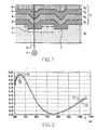
- the quality of such storage media depends essentially on the choice and compliance with the correct layer thicknesses in the layer system 2 the substrate 1 from. Therefore, it is necessary for quality control and / or during the coating process in the inline process the Thicknesses of the individual layers 3 to 6 should be determined as precisely as possible.
- This is achieved with the method according to the invention, wherein a light beam 8 of a light source 9 perpendicular to the applied Layers facing away from the substrate 1 on the substrate 1 is directed.
- the wavelength of the directed onto the substrate light beam 8 in a wavelength range changed from about 400 to 1100 nm.
- Figure 2 shows a diagram in which the reflectivity of a layer structure, as shown for example in Figure 1, is shown as a function of the wavelength of the incident light.
- the substrate 1 is planar, that is, it has no grooves, as shown in Figure 1.
- the curve 21 represents the calculated reflectivity and the curve 22 the measured reflectivity.
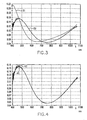
- the light losses in vertical incidence on the sample taking into account these light losses arise through the grooves of the substrate.
- the invention is preferably the in-phase superposition electromagnetic Partial waves at the grooves and thus their interference is calculated.
- the variations of Parameters also included the width b and the depth 7 of the grooves 7.
- a layer system 2 for a CD-RW layer 3 consisted of ZnSSiox, the layer 4 from AglnSbTe, layer 5 from ZnSSiox and layer 6 from ALTi. These layers were on a polycarbonate Substrate or blank 1 with grooves 7.
- FIG. 5 shows a measurement result for the determination of the groove depth t over a polycarbonate blank, which has grooves. There are no layers applied to the blank. Because of the difference Groove depths t over the substrate surface is it quickly and easily possible, production errors during injection molding of Determine substrates or blanks.
- the inventive method and based on this method Meter is with great advantage in production equipment for optical Storage media applicable.
- the reflection and / or transmission light intensity values are spectrally resolved, in the zeroth order of diffraction measured and from this either the layer thicknesses at the same time and determines the groove geometry or the layer thicknesses known groove geometry.
- actual sizes of the layer thicknesses of the target values are the values for the manipulated variables of the production plant, for example the sputtering rate and / or the sputtering time is newly determined or set and transmitted to the production facility.
Landscapes
- Physics & Mathematics (AREA)
- General Physics & Mathematics (AREA)
- Length Measuring Devices By Optical Means (AREA)
- Analysing Materials By The Use Of Radiation (AREA)
- Testing Or Measuring Of Semiconductors Or The Like (AREA)
Description
- Messen von Reflexions- und/oder Transmissions-Lichtintensitäts-Werten nullter Beugungsordnung in Abhängigkeit von der Wellenlänge,
- Berechnen der Reflexions- und/oder Transmissions-Lichtintensitäts-Werte unter Verwendung eines Iterationsmodells, in das die einzelnen Schichtparameter und die geometrischen Abmessungen der geometrischen Strukturen des Substrats als weitere Parameter eingehen, und
- Ändern der Schicht Parameter bis zur Herbeiführung einer Übereinstimmung zwischen den gemessenen und berechneten Werten.
- Fig. 1
- eine schematische Darstellung eines optischen Datenspeichers, bei dem das erfindungsgemäße Verfahren angewandt wird,
- Fig. 2 bis 4
- Diagramme bei denen über die Wellenlänge die Reflexions-Lichtintensitätswerte aufgetragen sind; und
- Fig. 5
- ein Ausführungsbeispiel zur Ermittlung der ortsaufgelösten Abmessungen der Substratstrukturen.
Claims (9)
- Verfahren zum Bestimmen der Dicke wenigstens einer Schicht (3 bis 6) auf einem Substrat (1), das zu Lichtbeugung führende geometrische Strukturen (7) aufweist, durchMessen von Reflexions- und/oder Transmissions-Lichtintensitäts-Werten nullter Beugungsordnung in Abhängigkeit von der Wellenlänge,Berechnen der Reflexions- und/oder Transmissions-Lichtintensitäts-Werte unter Verwendung eines Iterationsmodells, in das die einzelnen Schichtparameter und die geometrischen Abmessungen der geometrischen Strukturen (7) des Substrats (1) als weitere Parameter eingehen, undÄndern der Schichtparameter bis zur Herbeiführung einer Übereinstimmung zwischen den gemessenen und berechneten Werten.
- Verfahren nach Anspruch 1, dadurch gekennzeichnet, daß die geometrischen Abmessungen der Strukturen (7) bestimmt werden.
- Verfahren nach einem der vorhergehenden Ansprüche, dadurch gekennzeichnet, daß die ermittelten Daten der Schichtdicken (n) und/oder der geometrischen Struktur (7) zur Regelung von Fertigungsverfahren zum Aufbringen von wenigstens einer Schicht (3 bis 6) auf ein Substrat (1) und/oder zum Ausbilden von Substratstrukturen (7) herangezogen werden.
- Verfahren nach einem der vorhergehenden Ansprüche, dadurch gekennzeichnet, daß die Substrate (1) Rohlinge für Datenspeichermedien sind.
- Verfahren nach Anspruch 4, dadurch gekennzeichnet, daß geometrische Strukturen (7) als Rillen im Rohling ausgebildet sind.
- Verfahren nach einem der vorhergehenden Ansprüche, dadurch gekennzeichnet, daß wenigstens eine Schicht (3 bis 6) eine informationstragende Schicht (4) ist .
- Verfahren nach Anspruch 6, dadurch gekennzeichnet, daß die informationstragende Schicht (4) eine Metall-Legierung ist, die durch Energie-Einwirkung eines Lichtstrahls zwischen zwei Phasen veränderbar ist.
- Verfahren nach Anspruch 6 oder 7, dadurch gekennzeichnet, daß die informationstragende Schicht (4) zwischen zwei Buffer-Schichten (3, 5) ausgebildet ist.
- Verfahren nach einem der vorhergehenden Ansprüche, gekennzeichnet durch die Verwendung bei der Herstellung von optischen Datenspeicher-Medien.
Applications Claiming Priority (3)
| Application Number | Priority Date | Filing Date | Title |
|---|---|---|---|
| DE19852323A DE19852323C2 (de) | 1998-11-12 | 1998-11-12 | Verfahren zum Bestimmen der Dicke von auf einem Substrat vorgesehenen Schichten |
| DE19852323 | 1998-11-12 | ||
| PCT/EP1999/008534 WO2000029808A1 (de) | 1998-11-12 | 1999-11-06 | Verfahren zum bestimmen der dicke einer vielfach-dünnschichtstruktur |
Publications (2)
| Publication Number | Publication Date |
|---|---|
| EP1129322A1 EP1129322A1 (de) | 2001-09-05 |
| EP1129322B1 true EP1129322B1 (de) | 2005-01-12 |
Family
ID=7887649
Family Applications (1)
| Application Number | Title | Priority Date | Filing Date |
|---|---|---|---|
| EP99958007A Expired - Lifetime EP1129322B1 (de) | 1998-11-12 | 1999-11-06 | Verfahren zum bestimmen der dicke einer vielfach-dünnschichtstruktur |
Country Status (12)
| Country | Link |
|---|---|
| US (1) | US6744521B1 (de) |
| EP (1) | EP1129322B1 (de) |
| JP (1) | JP2002530632A (de) |
| KR (1) | KR100426045B1 (de) |
| CN (1) | CN1177194C (de) |
| AT (1) | ATE287078T1 (de) |
| CA (1) | CA2350511A1 (de) |
| DE (2) | DE19852323C2 (de) |
| ES (1) | ES2237180T3 (de) |
| IL (1) | IL143016A (de) |
| TW (1) | TW414858B (de) |
| WO (1) | WO2000029808A1 (de) |
Cited By (1)
| Publication number | Priority date | Publication date | Assignee | Title |
|---|---|---|---|---|
| EP3081901A1 (de) | 2015-04-17 | 2016-10-19 | Hennecke Systems GmbH | Inspektionsverfahren und vorrichtung zur inspektion einer oberflächenstruktur |
Families Citing this family (9)
| Publication number | Priority date | Publication date | Assignee | Title |
|---|---|---|---|---|
| DE19950559B4 (de) | 1999-10-20 | 2006-08-17 | Steag Eta-Optik Gmbh | Verfahren zum Bestimmen von geometrischen Strukturen auf oder in einem Substrat sowie von Materialparametern |
| US7049156B2 (en) * | 2003-03-19 | 2006-05-23 | Verity Instruments, Inc. | System and method for in-situ monitor and control of film thickness and trench depth |
| DE10346850B4 (de) * | 2003-10-09 | 2005-12-15 | Infineon Technologies Ag | Verfahren zum Ermitteln einer Eigenschaft einer strukturierten Schicht |
| JP4282500B2 (ja) * | 2004-01-29 | 2009-06-24 | 株式会社東芝 | 構造検査方法及び半導体装置の製造方法 |
| JP4639821B2 (ja) * | 2004-02-24 | 2011-02-23 | オムロン株式会社 | 目標値加工装置、温度調節器および制御プロセス実行システム |
| TWI302756B (en) * | 2004-04-19 | 2008-11-01 | Phoseon Technology Inc | Imaging semiconductor structures using solid state illumination |
| JP2006313077A (ja) * | 2005-05-06 | 2006-11-16 | Ricoh Co Ltd | 光学積層体検査方法,光学積層体製造方法および光学積層体検査装置ならびに光学積層体製造装置 |
| JP5186129B2 (ja) | 2006-08-25 | 2013-04-17 | 大日本スクリーン製造株式会社 | 溝パターンの深さの測定方法および測定装置 |
| CN102378909B (zh) * | 2009-04-30 | 2014-07-02 | 威尔科克斯联营公司 | 检查方法和检查装置 |
Family Cites Families (7)
| Publication number | Priority date | Publication date | Assignee | Title |
|---|---|---|---|---|
| DE4228870C2 (de) * | 1992-08-29 | 1997-01-09 | Inst Halbleiterphysik Gmbh | Verfahren zum Bestimmen geometrischer Abmessungen an dünnen, optisch transparenten Schichten |
| JPH074922A (ja) * | 1993-06-21 | 1995-01-10 | Jasco Corp | 半導体多層薄膜膜厚測定装置およびその測定方法 |
| US5604581A (en) * | 1994-10-07 | 1997-02-18 | On-Line Technologies, Inc. | Film thickness and free carrier concentration analysis method and apparatus |
| US5835226A (en) * | 1997-11-13 | 1998-11-10 | Lsi Logic Corporation | Method for determining optical constants prior to film processing to be used improve accuracy of post-processing thickness measurements |
| US5900633A (en) | 1997-12-15 | 1999-05-04 | On-Line Technologies, Inc | Spectrometric method for analysis of film thickness and composition on a patterned sample |
| IL123727A (en) * | 1998-03-18 | 2002-05-23 | Nova Measuring Instr Ltd | Method and apparatus for measurement of patterned structures |
| JP2000310512A (ja) | 1999-04-28 | 2000-11-07 | Hitachi Ltd | 薄膜の膜厚計測方法及びその装置並びにそれを用いた薄膜デバイスの製造方法及びその装置 |
-
1998
- 1998-11-12 DE DE19852323A patent/DE19852323C2/de not_active Expired - Fee Related
-
1999
- 1999-11-06 ES ES99958007T patent/ES2237180T3/es not_active Expired - Lifetime
- 1999-11-06 AT AT99958007T patent/ATE287078T1/de not_active IP Right Cessation
- 1999-11-06 CN CNB998132063A patent/CN1177194C/zh not_active Expired - Fee Related
- 1999-11-06 CA CA002350511A patent/CA2350511A1/en not_active Abandoned
- 1999-11-06 EP EP99958007A patent/EP1129322B1/de not_active Expired - Lifetime
- 1999-11-06 WO PCT/EP1999/008534 patent/WO2000029808A1/de not_active Ceased
- 1999-11-06 KR KR10-2001-7005969A patent/KR100426045B1/ko not_active Expired - Fee Related
- 1999-11-06 IL IL14301699A patent/IL143016A/en not_active IP Right Cessation
- 1999-11-06 US US09/831,842 patent/US6744521B1/en not_active Expired - Fee Related
- 1999-11-06 DE DE59911456T patent/DE59911456D1/de not_active Expired - Lifetime
- 1999-11-06 JP JP2000582762A patent/JP2002530632A/ja active Pending
- 1999-11-08 TW TW088119505A patent/TW414858B/zh not_active IP Right Cessation
Cited By (2)
| Publication number | Priority date | Publication date | Assignee | Title |
|---|---|---|---|---|
| EP3081901A1 (de) | 2015-04-17 | 2016-10-19 | Hennecke Systems GmbH | Inspektionsverfahren und vorrichtung zur inspektion einer oberflächenstruktur |
| WO2016166593A1 (en) | 2015-04-17 | 2016-10-20 | Hennecke Systems Gmbh | Inspection method and device for inspecting a surface pattern |
Also Published As
| Publication number | Publication date |
|---|---|
| DE19852323A1 (de) | 2000-05-31 |
| IL143016A0 (en) | 2002-04-21 |
| TW414858B (en) | 2000-12-11 |
| CA2350511A1 (en) | 2000-05-25 |
| US6744521B1 (en) | 2004-06-01 |
| KR20010086019A (ko) | 2001-09-07 |
| ES2237180T3 (es) | 2005-07-16 |
| JP2002530632A (ja) | 2002-09-17 |
| HK1056772A1 (en) | 2004-02-27 |
| DE19852323C2 (de) | 2001-08-16 |
| ATE287078T1 (de) | 2005-01-15 |
| IL143016A (en) | 2004-09-27 |
| KR100426045B1 (ko) | 2004-04-06 |
| CN1177194C (zh) | 2004-11-24 |
| DE59911456D1 (de) | 2005-02-17 |
| CN1429332A (zh) | 2003-07-09 |
| EP1129322A1 (de) | 2001-09-05 |
| WO2000029808A1 (de) | 2000-05-25 |
Similar Documents
| Publication | Publication Date | Title |
|---|---|---|
| DE4029912A1 (de) | Verfahren zur bildung mindestens eines grabens in einer substratschicht | |
| EP1129322B1 (de) | Verfahren zum bestimmen der dicke einer vielfach-dünnschichtstruktur | |
| DE69612794T2 (de) | Phasengitter, seine Herstellung, sowie optische Kodiereinrichtung, Motor mit einer solchen Kodiereinrichtung und Roboter mit einem solchen Motor | |
| DE2839535C2 (de) | Verfahren zur Herstellung eines Meßkörpers für Interferenzmessungen von Schichtdicken eines einkristallinen Körpers und Verwendung dieses Meßkörpers für die Herstellung eines Halbleiterkörpers | |
| DE3851370T2 (de) | Testvorrichtung zur Durchführung eines Realisierungsverfahrens von Halbleiterstrukturen. | |
| DE4419476A1 (de) | Verfahren und Vorrichtung zur Bestimmung von Schichtdicke und Substrattemperatur | |
| DE3851753T2 (de) | Verfahren zur herstellung von beugungsgittern geringen wirkungsgrades und ein dabei erhaltenes produkt. | |
| EP2331294A1 (de) | Verfahren zum messen der dicke eines scheibenförmigen werkstücks | |
| EP0629592A1 (de) | Verfahren zur Herstellung anorganischer diffraktiver Elemente und Verwendung derselben | |
| DE69426171T2 (de) | Optisches Informationsaufzeichnungsmedium | |
| DE112014005347T5 (de) | Herstellungsverfahren für integrierte Rechenelemente | |
| DE3910491C1 (de) | ||
| EP1012838B1 (de) | Verfahren zur regelung eines beschichtungsvorgangs | |
| EP2825859B1 (de) | Vorrichtung zum bestimmen der temperatur eines substrats | |
| DE4001506C2 (de) | Drei Verfahren zum Bestimmen des einzustellenden Meß-Einfallswinkels eines monochromatischen Meß-Lichtstrahls bei der Messung des Brechungsindex und der Dicke einer dünnen Schicht | |
| DE4440047C2 (de) | Verfahren zum Herstellen eines sich verjüngenden Wellenleiters | |
| DE19950559B4 (de) | Verfahren zum Bestimmen von geometrischen Strukturen auf oder in einem Substrat sowie von Materialparametern | |
| DE60222306T2 (de) | Verfahren zum Bestimmen einer Änderung des Durchlassgrades eines optischen Informationsaufzeichnungsmediums | |
| DE10227376B4 (de) | Verfahren zur Bestimmung von Schichtdickenbereichen | |
| DE2623687C3 (de) | Verfahren zum Messen der Dicke einer epitaxial auf ein Substrat aufgewachsenen Schicht | |
| WO2010037469A1 (de) | Verfahren zum messen der dicke von in einer bearbeitungsmaschine bearbeiteten scheibenförmigen werkstücken | |
| DE102012022343B4 (de) | Verfahren zum Überwachen eines Schichtwachstums und Vorrichtung zum Beschichten | |
| EP0425917B1 (de) | Verfahren zur Qualitätskontrolle von metallischen Oberflächen | |
| DE102015220307A1 (de) | Verfahren zum additiven Herstellen eines Bauteils, insbesondere eines Bauteils für ein Flugtriebwerk | |
| DE10244876A1 (de) | Messchip und Verfahren zu seiner Herstellung |
Legal Events
| Date | Code | Title | Description |
|---|---|---|---|
| PUAI | Public reference made under article 153(3) epc to a published international application that has entered the european phase |
Free format text: ORIGINAL CODE: 0009012 |
|
| 17P | Request for examination filed |
Effective date: 20010602 |
|
| AK | Designated contracting states |
Kind code of ref document: A1 Designated state(s): AT BE CH CY DE DK ES FI FR GB GR IE IT LI LU MC NL PT SE |
|
| GRAP | Despatch of communication of intention to grant a patent |
Free format text: ORIGINAL CODE: EPIDOSNIGR1 |
|
| GRAS | Grant fee paid |
Free format text: ORIGINAL CODE: EPIDOSNIGR3 |
|
| GRAA | (expected) grant |
Free format text: ORIGINAL CODE: 0009210 |
|
| AK | Designated contracting states |
Kind code of ref document: B1 Designated state(s): AT BE CH CY DE DK ES FI FR GB GR IE IT LI LU MC NL PT SE |
|
| PG25 | Lapsed in a contracting state [announced via postgrant information from national office to epo] |
Ref country code: FI Free format text: LAPSE BECAUSE OF FAILURE TO SUBMIT A TRANSLATION OF THE DESCRIPTION OR TO PAY THE FEE WITHIN THE PRESCRIBED TIME-LIMIT Effective date: 20050112 |
|
| REG | Reference to a national code |
Ref country code: GB Ref legal event code: FG4D Free format text: NOT ENGLISH |
|
| REG | Reference to a national code |
Ref country code: CH Ref legal event code: EP |
|
| BECA | Be: change of holder's address |
Owner name: *STEAG ETA-OPTIK G.M.B.H.BORSIGSTRASSE 78-80, D-52 Effective date: 20050112 |
|
| BECH | Be: change of holder |
Owner name: *STEAG ETA-OPTIK G.M.B.H. Effective date: 20050112 |
|
| REF | Corresponds to: |
Ref document number: 59911456 Country of ref document: DE Date of ref document: 20050217 Kind code of ref document: P |
|
| REG | Reference to a national code |
Ref country code: IE Ref legal event code: FG4D Free format text: GERMAN |
|
| PG25 | Lapsed in a contracting state [announced via postgrant information from national office to epo] |
Ref country code: DK Free format text: LAPSE BECAUSE OF FAILURE TO SUBMIT A TRANSLATION OF THE DESCRIPTION OR TO PAY THE FEE WITHIN THE PRESCRIBED TIME-LIMIT Effective date: 20050412 |
|
| REG | Reference to a national code |
Ref country code: SE Ref legal event code: TRGR |
|
| GBT | Gb: translation of ep patent filed (gb section 77(6)(a)/1977) |
Effective date: 20050414 |
|
| REG | Reference to a national code |
Ref country code: GR Ref legal event code: EP Ref document number: 20050401197 Country of ref document: GR |
|
| RAP2 | Party data changed (patent owner data changed or rights of a patent transferred) |
Owner name: STEAG ETA-OPTIK GMBH |
|
| REG | Reference to a national code |
Ref country code: CH Ref legal event code: PUE Owner name: STEAG ETA-OPTIK GMBH Free format text: STEAG HAMATECH AG#FERDINAND-VON-STEINBEIS-RING 10#75447 STERNENFELS (DE) -TRANSFER TO- STEAG ETA-OPTIK GMBH#BORSIGSTRASSE 78-80#52525 HEINSBERG (DE) Ref country code: CH Ref legal event code: NV Representative=s name: KELLER & PARTNER PATENTANWAELTE AG |
|
| REG | Reference to a national code |
Ref country code: ES Ref legal event code: FG2A Ref document number: 2237180 Country of ref document: ES Kind code of ref document: T3 |
|
| REG | Reference to a national code |
Ref country code: GB Ref legal event code: 732E |
|
| NLT2 | Nl: modifications (of names), taken from the european patent patent bulletin |
Owner name: STEAG ETA-OPTIK GMBH |
|
| NLS | Nl: assignments of ep-patents |
Owner name: STEAG ETA-OPTIK GMBH Effective date: 20050802 |
|
| PG25 | Lapsed in a contracting state [announced via postgrant information from national office to epo] |
Ref country code: CY Free format text: LAPSE BECAUSE OF FAILURE TO SUBMIT A TRANSLATION OF THE DESCRIPTION OR TO PAY THE FEE WITHIN THE PRESCRIBED TIME-LIMIT Effective date: 20051106 Ref country code: AT Free format text: LAPSE BECAUSE OF NON-PAYMENT OF DUE FEES Effective date: 20051106 |
|
| PG25 | Lapsed in a contracting state [announced via postgrant information from national office to epo] |
Ref country code: SE Free format text: LAPSE BECAUSE OF NON-PAYMENT OF DUE FEES Effective date: 20051107 Ref country code: IE Free format text: LAPSE BECAUSE OF NON-PAYMENT OF DUE FEES Effective date: 20051107 Ref country code: ES Free format text: LAPSE BECAUSE OF NON-PAYMENT OF DUE FEES Effective date: 20051107 |
|
| PLBE | No opposition filed within time limit |
Free format text: ORIGINAL CODE: 0009261 |
|
| STAA | Information on the status of an ep patent application or granted ep patent |
Free format text: STATUS: NO OPPOSITION FILED WITHIN TIME LIMIT |
|
| PG25 | Lapsed in a contracting state [announced via postgrant information from national office to epo] |
Ref country code: MC Free format text: LAPSE BECAUSE OF NON-PAYMENT OF DUE FEES Effective date: 20051130 Ref country code: LU Free format text: LAPSE BECAUSE OF NON-PAYMENT OF DUE FEES Effective date: 20051130 Ref country code: LI Free format text: LAPSE BECAUSE OF NON-PAYMENT OF DUE FEES Effective date: 20051130 Ref country code: CH Free format text: LAPSE BECAUSE OF NON-PAYMENT OF DUE FEES Effective date: 20051130 Ref country code: BE Free format text: LAPSE BECAUSE OF NON-PAYMENT OF DUE FEES Effective date: 20051130 |
|
| ET | Fr: translation filed | ||
| 26N | No opposition filed |
Effective date: 20051013 |
|
| PG25 | Lapsed in a contracting state [announced via postgrant information from national office to epo] |
Ref country code: NL Free format text: LAPSE BECAUSE OF NON-PAYMENT OF DUE FEES Effective date: 20060601 |
|
| REG | Reference to a national code |
Ref country code: CH Ref legal event code: PL |
|
| EUG | Se: european patent has lapsed | ||
| NLV4 | Nl: lapsed or anulled due to non-payment of the annual fee |
Effective date: 20060601 |
|
| REG | Reference to a national code |
Ref country code: IE Ref legal event code: MM4A |
|
| PGFP | Annual fee paid to national office [announced via postgrant information from national office to epo] |
Ref country code: FR Payment date: 20061124 Year of fee payment: 8 |
|
| PGFP | Annual fee paid to national office [announced via postgrant information from national office to epo] |
Ref country code: GB Payment date: 20061127 Year of fee payment: 8 |
|
| PGFP | Annual fee paid to national office [announced via postgrant information from national office to epo] |
Ref country code: IT Payment date: 20061130 Year of fee payment: 8 |
|
| REG | Reference to a national code |
Ref country code: ES Ref legal event code: FD2A Effective date: 20051107 |
|
| BECA | Be: change of holder's address |
Owner name: *STEAG ETA-OPTIK G.M.B.H.BORSIGSTRASSE 78-80, D-52 Effective date: 20050112 |
|
| BECH | Be: change of holder |
Owner name: *STEAG ETA-OPTIK G.M.B.H. Effective date: 20050112 |
|
| BERE | Be: lapsed |
Owner name: *STEAG ETA-OPTIK G.M.B.H. Effective date: 20051130 |
|
| PG25 | Lapsed in a contracting state [announced via postgrant information from national office to epo] |
Ref country code: PT Free format text: LAPSE BECAUSE OF NON-PAYMENT OF DUE FEES Effective date: 20050612 |
|
| PG25 | Lapsed in a contracting state [announced via postgrant information from national office to epo] |
Ref country code: GR Free format text: LAPSE BECAUSE OF NON-PAYMENT OF DUE FEES Effective date: 20050112 |
|
| GBPC | Gb: european patent ceased through non-payment of renewal fee |
Effective date: 20071106 |
|
| REG | Reference to a national code |
Ref country code: FR Ref legal event code: ST Effective date: 20080930 |
|
| PG25 | Lapsed in a contracting state [announced via postgrant information from national office to epo] |
Ref country code: GB Free format text: LAPSE BECAUSE OF NON-PAYMENT OF DUE FEES Effective date: 20071106 |
|
| PG25 | Lapsed in a contracting state [announced via postgrant information from national office to epo] |
Ref country code: FR Free format text: LAPSE BECAUSE OF NON-PAYMENT OF DUE FEES Effective date: 20071130 |
|
| PG25 | Lapsed in a contracting state [announced via postgrant information from national office to epo] |
Ref country code: IT Free format text: LAPSE BECAUSE OF NON-PAYMENT OF DUE FEES Effective date: 20071106 |
|
| PGFP | Annual fee paid to national office [announced via postgrant information from national office to epo] |
Ref country code: DE Payment date: 20151119 Year of fee payment: 17 |
|
| REG | Reference to a national code |
Ref country code: DE Ref legal event code: R119 Ref document number: 59911456 Country of ref document: DE |
|
| PG25 | Lapsed in a contracting state [announced via postgrant information from national office to epo] |
Ref country code: DE Free format text: LAPSE BECAUSE OF NON-PAYMENT OF DUE FEES Effective date: 20170601 |