EP1132993A2 - Résonateur, filtre, oscillateur, duplexeur et dispositif de communication - Google Patents
Résonateur, filtre, oscillateur, duplexeur et dispositif de communication Download PDFInfo
- Publication number
- EP1132993A2 EP1132993A2 EP01105154A EP01105154A EP1132993A2 EP 1132993 A2 EP1132993 A2 EP 1132993A2 EP 01105154 A EP01105154 A EP 01105154A EP 01105154 A EP01105154 A EP 01105154A EP 1132993 A2 EP1132993 A2 EP 1132993A2
- Authority
- EP
- European Patent Office
- Prior art keywords
- slot
- resonator
- electrode
- shaped opening
- electrode patterns
- Prior art date
- Legal status (The legal status is an assumption and is not a legal conclusion. Google has not performed a legal analysis and makes no representation as to the accuracy of the status listed.)
- Withdrawn
Links
Images



Classifications
-
- H—ELECTRICITY
- H01—ELECTRIC ELEMENTS
- H01P—WAVEGUIDES; RESONATORS, LINES, OR OTHER DEVICES OF THE WAVEGUIDE TYPE
- H01P7/00—Resonators of the waveguide type
- H01P7/08—Strip line resonators
-
- H—ELECTRICITY
- H01—ELECTRIC ELEMENTS
- H01P—WAVEGUIDES; RESONATORS, LINES, OR OTHER DEVICES OF THE WAVEGUIDE TYPE
- H01P1/00—Auxiliary devices
- H01P1/20—Frequency-selective devices, e.g. filters
- H01P1/201—Filters for transverse electromagnetic waves
- H01P1/2016—Slot line filters; Fin line filters
-
- H—ELECTRICITY
- H01—ELECTRIC ELEMENTS
- H01P—WAVEGUIDES; RESONATORS, LINES, OR OTHER DEVICES OF THE WAVEGUIDE TYPE
- H01P1/00—Auxiliary devices
- H01P1/20—Frequency-selective devices, e.g. filters
- H01P1/213—Frequency-selective devices, e.g. filters combining or separating two or more different frequencies
- H01P1/2135—Frequency-selective devices, e.g. filters combining or separating two or more different frequencies using strip line filters
Definitions
- the present invention relates to a resonator having an electrode formed on a dielectric substrate, a filter, an oscillator, a duplexer, and a communication apparatus employing these devices.
- Resonators formed using a dielectric substrate and designed to exhibit resonance in the frequency band of microwaves or millimeter waves include a resonator realized with a slot line.
- one resonator is realized with a straight half-wave slot line.
- Such a resonator realized with a slot line is structured to have an electrode continuously formed around a slot line, and can therefore confine electromagnetic energy in the slot line with high efficiency.
- the resonator is included as a module in a high-frequency circuit, it hardly interferes with any other circuit. This is advantageous.
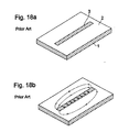
- Fig. 18A and Fig. 18B show an example of a half-wave slot-line resonator having both ends thereof short-circuited.
- an electrode 2 having a slot 3 bored as part thereof is formed on the upper side of a dielectric substrate 1.
- Fig. 18B shows the distribution of the electromagnetic field on the slot-line resonator.
- solid lines denote the electric field and dashed lines denote the magnetic field.
- the efficiency of the resonator realized with a slot line in confining the electromagnetic field depends on the width of the slot. In other words, the larger the width of the slot 3 (slot line), the wider the spread of the electromagnetic field in the slot-line resonator.
- the electric field distribution in a slotted section is as shown in Fig. 19A.
- the equivalent circuit is like that shown in Fig. 19B or Fig. 19C.
- Fig. 19B shows an equivalent circuit for a large-width slot
- Fig. 19C shows an equivalent circuit for a small-width slot.
- the ratio of an electrostatic capacitance C2 (C2') or C3 (C3') to the total electrostatic capacitance is large, or in other words, if the electrostatic capacitance C2 (C2') or C3 (C3') contributes greatly to the total electrostatic capacitance, the spread of the electromagnetic field is thought to be wide.
- the ratio is small or if the electrostatic capacitance C2 (C2') or C3 (C3') contributes little, the degree of concentration of the electromagnetic field in the slot is thought to be high.
- a high-frequency circuit module is assumed to be composed of a slot-linc resonator and another conductive line which are formed using a dielectric substrate. In this case, once the efficiency of the slot-line resonator in confining the electromagnetic field is improved, even if the distance from the slot-line resonator to the conductive line is decreased, undesirable coupling will hardly occur.
- the high-frequency circuit module can therefore be designed compactly.
- the present invention provides a resonator, a filter, an oscillator, a duplexer, and a communication apparatus employing these devices which exhibit improved efficiency in confining an electromagnetic field in an opening of an electrode, suppressed concentration of currents, and minimized conductor loss.
- a resonator has a slot-like opening formed in a dielectric substrate. Electrode patterns are formed in the slot-like opening so that the slot-like opening will be divided into smaller-width slot lines. The electrode patterns by which the slot-like opening is divided into the smaller-width slot lines have a width permitting suppression of an edge effect occurring in the electrode patterns.
- the resonator is structured to have a plurality of slot lines, which serve as resonators, juxtaposed and separated by the electrode patterns.
- the direction of a current flowing along one edge of each of the electrode patterns by which the slot-like opening is divided into the smaller-width slot lines is opposite to the direction of a current flowing along the other parallel edge thereof.
- the currcots flow close to each other in mutually opposite directions. Therefore, loss hardly occurs in each electrode pattern. However, conductor loss occurs at both the edges of each electrode pattern.
- the electrode patterns are preferably formed only in short-circuited or equivalently short-circuited portions of the slot-like opening so that adjoining slot lines will communicate with a portion of the slot-like opening. Owing to this structure, conduction loss occurring in part of eacb electrode pattern which exhibits a high current density is minimized effectively. Moreover, the adjoining slot lines into which the slot-like opening is divided communicate with the portion of the slot-like opening devoid of the electrode patterns. Consequently, occurrence of a spurious pulse mode in each of the slot lines into which the slot-like opening is divided by the electrode patterns can be suppressed. Moreover, a portion of the slot-like opening in which the electrode patterns, by which the slot-like opening is divided into the smaller-width slot lines, are formed is so limited that the electrode patterns can be formed easily.
- the slot-like opening in the resonator is preferably shaped spirally. Consequently, currents flowing along edges formed between two adjoining lines of the slot lines, into which the spiral slot-like opening is divided, are canceled out. Conductor loss occurring at the edges between the slot lines can be minimized more effectively.
- a plurality of slot-like openings is juxtaposed in the resonator, and the width of each slot-like opening is made larger near an equivalently open position.
- Electrode patterns are formed at short-circuited or equivalently short-circuited positions in each slot-like opening so that the slot-like opening will be divided into smaller-width slot lines, whereby the spread of the magnetic field is suppressed.
- the slot-like openings are juxtaposed, the degree of coupling among the openings decreases.
- electric fields are dominant near the equivalently open position in each slot-like opening. Therefore, since the plurality of slot-like openings whose widths are each made larger near the equivalently open position is juxtaposed, the degree of coupling between adjoining slot-like openings can be increased.
- an electrode having an opening as part thereof may be formed on a dielectric substrate, and a plurality of electrode patterns may be extended inwards from the periphery of the opening so that a plurality of slot lines will be arranged substantially radially.
- the electrode patterns extended inwards have a sufficiently small width.
- the direction of a current flowing along one edge of each of the plurality of electrode patterns is opposite to the direction of a current flowing along the other edge thereof parallel to the one edge. Therefore, edge effects are canceled out.
- the slot lines are arranged substantially radially, each of the slot lines adjoins another slot line. The slot lines do not have an edge at which an edge effect occurs. Compared with a resonator realized with a single slot line, the overall conductor loss is suppressed.
- a filter includes a resonator having any of the aforesaid structures, and a signal input/output port.
- an oscillator is a band reflection type oscillator comprising a reflex amplification circuit and the aforesaid resonator.
- the stability in an oscillation frequency is improved by utilizing the property of a resonator that is a high unloaded Q-factor Qo.
- a duplexer is provided with the aforesaid filter as a transmission filter and a reception filter respectively connected between a transmission signal input port and an input/output port used in common for transmission and reception, and between the input/output port used in common for transmission and reception and a reception signal output port.
- a communication apparatus is provided with the aforesaid resonator, filter, oscillator, or duplexer.
- a communication apparatus having a small loss and exhibiting high efficiency in utilizing power is provided by making the most of the property of a resonator that is a high unloaded Q-factor Qo. Moreover, since a resonator, a filter, an oscillator, or a duplexer which can highly efficiently confine electromagnetic fields is adopted, these devices and other circuits or devices can be located close to each other. The communication apparatus can therefore be designed compactly.
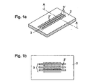
- Fig. 1A is a perspective view of a resonator
- Fig. 1B is a plan view showing an example of the current distribution.
- a dielectric substrate 1 has an electrode 2 formed on an upper side thereof, in which a rectangular slot 3 is machined. Electrode patterns 2' are formed so that the slot 3 is divided into smaller-width slot lines 3'. The slot lines 3' into which the slot 3 is finely divided by the electrode patterns 2' each operate as a half-wave resonator having both ends thereof short-circuited.
- the resonator shown in Fig. 1 Since the slot 3 in the resonator shown in Fig. 1 is divided into the slot lines 3' by the electrode patterns 2', the width of each slot line is smaller than that in the conventional resonator shown in Fig. 19A to Fig. 19C. Therefore, the resonator shown in Fig, 1 enjoys improved efficiency of confining the electromagnetic field.
- the resonator can be said to have three half-wave resonators juxtaposed therein.
- the three half-wave resonators are thought to be mutually coupled. Consequently, current concentration is alleviated and conductor loss is minimized.
- Fig. 1B the direction of a current flowing along one edge of each electrode pattern 2' is opposite to the direction of a current flowing along the other edge thereof. Current concentration at the edge is therefore alleviated. Consequently, almost no current flows through eacb electrode pattern 2'.
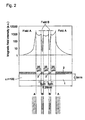
- the distribution of magnetic field intensities was calculated using a finite element method (FEM).
- FEM finite element method
- the upper graph shows the distribution of magnetic field intensities
- the middle diagram shows the slotted section of the resonator including the sections of the three parallel slot lines
- the lower diagram is a plan view of the slotted section.
- the electrode patterns including the edges at which magnetic fields are concentrated, define fields B which are disposed between two adjoining slot lines and fields A in which the effect of the presence of the slot lines is reduced.
- the concentration of the magnetic field sharply reduced in the fields B. The current density between the adjoining slot lines is therefore very low, and conductor loss occurring in the electrode patterns 2' is minimized drastically.
- the foregoing advantage can be expected even when the number of electrode patterns is three or more.
- no electrode is formed on the lower side of the dielectric substrate.
- a ground electrode may be formed all over the lower side of the dielectric substrate.
- an electrode having a slot and electrode patterns may be formed on the lower side of the dielectric substrate so that the slot and electrode patterns will be opposed (mirror-symmetric) to the slot 3 and electrode patterns 2' on the upper side thereof.
- the resonator operates as a resonator having a planar dielectric transmission line (PDTL), that is, having both the sides of the dielectric substrate sandwiched between the slots.
- PDTL planar dielectric transmission line
- Fig. 3A is a perspective view of a resonator
- Fig. 3B is a plan view showing an example of the current distribution.
- a dielectric substrate 1 has an electrode 2 formed on the upper side thereof; in which a slot 3 is machined. Electrode patterns 2' are extended inwards from short-circuited ends or equivalently short-circuited ends of the slot 3 so that the electrode patterns 2' divide the slot 3 into slot lines 3'.
- the resonator operates as a half-wave resonator having both ends thereof short-circuited.
- the electrode patterns 2' are formed as shown in Fig. 3A and Fig. 3B so that the slot 3 will be divided into slot lines at least near the short-circuited ends thereof.
- the efficiency of the resonator in confining the magnetic field is improved.
- the electrode patterns 2' are formed as shown in Fig. 3A and Fig. 3B so that the slot 3 will be divided into slot lines at least near the short-circuited ends thereof. Consequently, current concentration is alleviated.
- the direction of a current flowing along one edge of each of the electrode patterns 2' extended from the short-circuited ends of the slot is opposite to the direction of a current flowing along the other edge thereof. Therefore, almost no conductor loss occurs in the electrode patterns 2'. Consequently, the conductor loss occurring in the whole resonator is minimized.
- Fig. 4A and Fig. 4B are perspective views showing the magnetic field distribution with lines indicating equal magnetic field intensities.
- Fig. 5A and Fig. 5B are sectional views showing sections perpendicular to the direction in which the slot extends, showing magnetic field distributions with the lines indicating equal magnetic field intensities.
- Fig. 4A and Fig. 5A are concerned with the resonator in accordance with the second embodiment, while Fig. 4B and Fig. 5B are concerned with the conventional slot-line resonator.
- the thickness of the dielectric substrate is 0.6 mm
- the relative dielectric constant thereof is 24
- the distance to an upper or lower shield plate placed parallel to the dielectric substrate is 1.0 mm.
- the resonant frequency at which the resonator, with which Fig. 4A and Fig. 5A are concerned, exhibits resonance is 38 GHz.
- the resonant frequency at which the conventional resonator, with which Fig. 4B and Fig. 5B are concerned, exhibits resonance is 37.8 GHz.
- the clectrode patterns are formed to divide the slot into the slot lines in the width direction of the slot, the efficiency of the resonator in confining the electromagnetic field is improved.
- Fig. 3A and Fig. 3B, and other drawings show an example in which no electrode is formed on the lower side of the dielectric substrate.
- an electrode having a slot and electrode patterns may be formed on the lower side of the dielectric substrate so that the slot and electrode patterns will be opposed to the slot 3 and electrode patterns 2' formed on the upper side thereof.
- a resonator having a planar dielectric transmission line (PDTL) may be constructod.
- an electrode 2 having a slot 3 machined therein is formed on the upper side of a dielectric substrate 1.
- the slot 3 is open at both ends of the dielectric substrate 1, and operates as a half-wave resonator having both ends left open.
- electrode patterns 2' are formed in the center of the slot, that is, near an equivalently short-circuited position in the slot so that the slot 3 will be divided into smaller-width slot lines 3'. If the electrode patterns 2' were not present, the current density would be higher near the equivalently short-circuited position along the edges of the slot 3.
- the electrode patterns 2' are formed at the equivalently short-circuited position, current concentration is alleviated in the same manner as that in the aforesaid embodiment. Consequently, the unloaded Q-factor Qo of the resonator can be improved. Moreover, the slot is divided into smaller-width slot lines by the electrode patterns 2', though only part of the slot is divided. Therefore, the efficiency in confining the electromagnetic field is improved.
- one end of the slot 3 is short-circuited, and the other end thereof is left open.
- the slot 3 thus operates as a three-quarter-wave resonator.
- electrode patterns 2' are formed near equivalently short-circuited positions in the slot so that the slot 3 will be divided into smaller-width slot lines. Consequently, the efficiency of the resonator in confining the electromagnetic field is improved without a decrease in the unloaded Q-factor Qo of the resonator.
- an electrode 2 having a slot 3 with one end short-circuited and the other end left open is formed on the upper side of a dielectric substrate 1.
- Electrode patterns 2' having a length (1/2+ ⁇ ) ⁇ g are extended from the open end, where ⁇ denotes any value equal to or smaller than 1/4.
- the electrode patterns 2' are equivalent to the two sets of electrode patterns 2' shown in Fig. 6B. Even when a resonator has this structure, the efficiency of the resonator in confining the electromagnetic field can be improved without a decrease in the unloaded Q-factor Qo thereof.
- Fig. 7 shows the structure of a resonator in accordance with a fourth embodiment.
- an electrode 2 having a slot 3 with both ends left open is formed on the upper side of a dielectric substrate 1.
- the open portions of the slot are formed by machining round openings in the electrode.
- Slot lines formed between the two round openings operate as a resonator.
- Electrode patterns 2' are formed to divide the slot 3 into slot lines. Owing to the structure, the conductor loss occurring in the slot lines is minimized and the efficiency in confining the electromagnetic field is improved.
- Fig. 8 shows the structure of a resonator in accordance with a fifth embodiment.
- an electrode 2 having a slot 3 whose length is ⁇ g is formed on the upper side of a dielectric substrate 1.
- this example adopts a double-wave resonant mode. Both ends of the slot and the center thereof are therefore designed to be equivalently short-circuited positions. Electrode patterns 2' are formed near the equivalently short-circuited positions so that the slot 3 will be divided into smaller-width slot lines.
- an electrode 2 having slots 3a and 3b of a predetermined shape machined therein is formed on the upper side of a dielectric substrate 1.
- the slots 3a and 3b operate as double-wavc resonators having both ends thereof shortcircuited.
- the two slots are located adjacently to each other and are thus coupled to each other.
- Central electrode patterns 4a and 4b are formed in directions perpendicular to the longitudinal directions of the slots 3a and 3b respectively.
- the central electrode patterns 4a and 4b and electrode patterns 2' located on both sides of the central electrode pattern constitute a coplanar conductive line.
- the central electrode patterns 4a and 4b included in the coplanar lines are magnetically coupled to the associated slots.
- the coplanar lines are used as signal input and output lines.
- the filter acts as a bandpass filter having two resonators coupled to each other.
- Fig. 10 shows an example of a filter in accordance with a seventh embodiment.
- an electrode 2 having spiral slots 3 machined therein is formed on the upper side of a dielectric substrate 1.
- One end of each slot is short-cirouited.
- Electrode patterns 2' are extended from the short-circuited ends of the slots by a predetermined length so that the slots will each he divided into smaller-width slot lines. Consequently, the efficiency in confining the electromagnetic field is high. Moreover, unnecessary coupling to outside and unnecessary radiation to outside can be suppressed.
- currents flowing along edges of the electrode between adjoining lines of the spiral slot lines are canceled out. Conductor loss occurring at the edges of the electrode between the adjoining slot lines can be minimized. This results in a resonator exhibiting a higher unloaded Q-factor Qo.
- the spiral slots are symmetric to each other with respect to a straight line between the spiral slots.
- a central electrode pattern 4 is extended in a direction perpendicular to the longitudinal directions of the slots between the equivalently open ends of the slots located in the center of the electrode.
- a coplanar line composed of the central electrode pattern 4 and the electrode 2 extended on both sides of the central electrode pattern is magnetically coupled to the slots operating as resonators.
- An input/output port defined by the coplanar line is coupled to a predetermined conductive line, whereby this filter acts as a trap for attenuating a signal whose frequency is equivalent to a resonant frequency at which the slots operating as resonators exhibit resonance.
- Fig. 11 shows the structure of a resonator in accordance with an eighth embodiment.
- An electrode 2 having slots 3a, 3b, and 3c machined therein is formed on the upper side of a dielectric substrate.
- Electrode patterns 2' are extended from the equivalently short-circuit ends of the slots so that the slots will each be divided into smaller-width slot lines.
- the adjoining slots among the three slots operating as resonators are electromagnetically coupled to each other.
- the electrode patterns 2' work to diminish the spread of the magnetic field. Therefore, the coupling between adjoining slots is weaker than it would be if the adjoining slots were devoid of the electrode patterns 2'. However, since the central portions of the slots in which are dominant are made thicker as shown in Fig. 11, the electrical coupling between adjoining slots is strong.
- Fig. 12A is a perspective view
- Fig. 12B is a plan view
- An electrode 2 having a round opening 6 machined therein is formed on the upper side of a dielectric substrate 1.
- Electrode patterns 2' are extended inwards (radially) from the periphery of the round opening 6. Owing to the structure, a plurality of slot lines is arranged radially from the center of the opening.
- the opening is thus radially divided into the plurality of smaller-width slot lines, whereby the efficiency in confining the magnetic field is improved. Moreover, concentration of currents near a short-circuited end of the opening 6, that is, near the circumference of the opening 6, is alleviated.
- the direction of a current flowing along one edge of each electrode pattern 2' is, as shown in Fig. 12B, opposite to that of a current flowing along the other edge thereof. Almost no current flows through the electrode patterns 2'. Consequently, a conductor loss is minimized and the unloaded Q-factor Qo exhibited by the resonator is improved.
- the resonator would act as a resonator that utilizes a TE 010 mode.
- the resonator having the slot lines arranged radially utilizes a resonant mode different from the TE 010 -mode resonator.
- the area of the opening 6 in the resonator of Figs. 12A and 12B is a quarter or less of that in a TE 010 -mode resonator having the same resonant frequency.
- the resonator can therefore be designed to be much more compact than the TE 010 -mode resonator.
- Fig. 6A to Fig. 12B show examples in which no electrode is formed on the lower side of a dielectric substrate.
- a ground electrode may be formed all over the lower side of the dielectric substrate.
- an electrode having a slot and electrode patterns may be formed on the lower side of the dielectric substrate so that the slot and electrode patterns will be opposed to the slot 3 and electrode patterns 2' on the upper side thereof. This results in a resonator having a planar dielectric transmission line (PDTL).
- PDTL planar dielectric transmission line
- resonators R1, R2, and R3 are formed on the upper side of a dielectric substrate. These resonators are slots each of which is the same as the opening shown in Fig. 12A and Fig. 12B, and has a plurality of slot lines arranged radially. Moreover, on the upper side of the dielectric substrate, central electrode patterns 4a and 4b and an electrode extended around them constitute a coplanar line.
- Adjoining resonators of the resonators R1, R2, and R3 are magnetically coupled to each other. Moreover, the central electrode patterns 4a and 4b are magnetically coupled to the resonators R1 and R3. Consequently, the filter acts as a bandpass filter composed of the three resonators.
- openings may be machined in the lower side of the dielectric substrate so that the openings will be opposed to the slots operating as the resonators R1, R2, and R3.
- a ground electrode may be formed all over the lower side or no electrode may be formed on the lower side.
- Fig. 14 shows an example of the structure of a duplexer in accordance with an eleventh embodiment.
- a transmission filter and a reception filter are realized with dielectric resonators each composed of adjoining resonators each of which has two spiral slots identical to those shown in Fig. 10.
- the transmission filter is characterized in that it passes a transmission frequency band and attenuates a reception frequency band.
- the reception filter is characterized in that it passes the reception frequency band and attenuates the transmission frequency band.
- a transmission signal input port Tx a reception signal output port Rx, and an input/output port ANT used in common for transmission and reception.
- Transmission lines coupled to the ports are coplanar lines.
- a branch circuit is realized with the ANT port, the last-stage (second-stage) resonator of the transmission filter, and the initial-stage (first-stage) resonator of the reception filter which are interconnected over a coplanar line.
- the duplexer is also used as an antenna sharing device for a communication apparatus.
- a resonator R is a slot identical to the opening shown in Fig. 12A and Fig. 12B.
- a conductive line 5 is extended near the resonator R
- the conductive line 5 and an electrode 2 extended on both sides of the conductive line constitute a coplanar line, and the coplanar line is magnetically coupled to the resonator R.
- One end of the conductive line 5 is terminated with a termination resistor 8, and the other end thereof is coupled to a field-effect transistor (FET) 7.
- FET field-effect transistor
- a feedback circuit including the resonator is connected between the drain and gate of the FET 7.
- the resonator R has a band rejection characteristic.
- the distance between the resonator R and the FET 7 is set to a suitable value, whereby the oscillator oscillates at the same frequency as the resonant frequency of the resonator R.
- Another conductive line may be laid on the dielectric substrate shown in Fig. 15 so that it will be coupled to the resonator R.
- a variable-reactance device such as a varactor diode may then be connected to the conductive line.
- a circuit may be included for applying a control voltage to the variable-reactance device. This results in a voltage-controlled oscillator.
- the resonator R enjoys high efficiency in confining the electromagnetic field, the distance between the conductive line coupled to the FET 7 or the electrode and the resonator R may be decreased. Nevertheless, since the coupling between the conductive line or the electrode and the resonator is weak, the oscillator can be constructed on a limited-size dielectric substrate. The oscillator can be designed to be compact.
- slots 3 and 3' are machined on the upper side of a dielectric substrate 1. Slots having the same shapes as the slots 3 and 3' are machined on the lower side thereof so that they will be opposed to the slots 3 and 3'. Shield plates 9 and 10 are placed above and below the dielectric substrate 1.
- the slots 3 machined in the upper and lower sides of the dielectric substrate I and the upper and lower shield plates 9 and 10 operate as planar dielectric transmission lines (PDTL).
- the slots 3' and the upper and lower shield plates 9 and 10 constitute half-wave resonators each including a planar dielectric transmission line (PDTL) and having both ends thereof short-circuited.
- Electrode patterns 2' are extended from the short-circuited ends of each slot 3' so that the slot 3' will be divided into smaller-width slot lines. Consequently, the filter acts as a filter having resonators, which exhibit a high unloaded Q-factor Qo, connected by slot lines.
- the foregoing structure may be adapted to a generally known fin waveguide.
- the filter acts as a filter having resonators connected by transmission lines that are the fin waveguides.
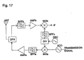
- Fig. 17 is a block diagram showing the configuration of a communication apparatus in accordance with a fourteenth embodiment.
- a transmission/reception antenna ANT a duplexer DPX, bandpass filters BPFa, BPFb, and BPFc, amplification circuits AMPa and AMPb, mixers MIXa and MIXb, an oscillator OSC, and a distributor DIV.
- a voltage-controlled oscillator VCO modulates an oscillation frequency according to a transmission signal (transmission data).
- the mixer MTXa mixes a signal modulated by the voltage-controlled oscillator VCO with a signal output from the oscillator OSC and distributed from the distributor DIV.
- the bandpass filter BPFa passes a component of the mixed output signal output from the mixer MIXa which falls within a transmission band.
- the amplification circuit AMPa amplifies in power a signal output from the bandpass filter BPFa.
- the resultant signal is transmilled from the antenna ANT via the duplexer DPX.
- the bandpass filter BPFb passes a component of a reception signal output from the duplexer DPX which falls within a reception band.
- the amplification circuit AMPb amplifies a signal output from the bandpass filter BPFb.
- the mixer MTXb mixes the fraquency component, which is output from the oscillator OSC, distributed from the distributor DIV, and output from the bandpass filter BPFc, with the reception signal, and outputs an intermediate-frequency signal IF.
- the duplexer shown in Fig. 14 may be adopted as the duplexer DPX shown in Fig. 17.
- the filter shown in Fig. 9, Fig. 10, or Fig. 13 or a filter composed of the resonator shown in any of Fig. 1A to Fig. 12B and a signal input/output unit may be adopted as the bandpass filters BPFa, BPFb, and BPFc.
- a voltage-controlled oscillator realized with the oscillator shown in Fig. 15 is adopted as the voltage-controlled oscillator VCO.
Landscapes
- Physics & Mathematics (AREA)
- Electromagnetism (AREA)
- Control Of Motors That Do Not Use Commutators (AREA)
- Inductance-Capacitance Distribution Constants And Capacitance-Resistance Oscillators (AREA)
Applications Claiming Priority (2)
| Application Number | Priority Date | Filing Date | Title |
|---|---|---|---|
| JP2000061954 | 2000-03-07 | ||
| JP2000061954A JP3521834B2 (ja) | 2000-03-07 | 2000-03-07 | 共振器、フィルタ、発振器、デュプレクサおよび通信装置 |
Publications (2)
| Publication Number | Publication Date |
|---|---|
| EP1132993A2 true EP1132993A2 (fr) | 2001-09-12 |
| EP1132993A3 EP1132993A3 (fr) | 2001-11-14 |
Family
ID=18582025
Family Applications (1)
| Application Number | Title | Priority Date | Filing Date |
|---|---|---|---|
| EP01105154A Withdrawn EP1132993A3 (fr) | 2000-03-07 | 2001-03-02 | Résonateur, filtre, oscillateur, duplexeur et dispositif de communication |
Country Status (3)
| Country | Link |
|---|---|
| US (2) | US6661315B2 (fr) |
| EP (1) | EP1132993A3 (fr) |
| JP (1) | JP3521834B2 (fr) |
Families Citing this family (8)
| Publication number | Priority date | Publication date | Assignee | Title |
|---|---|---|---|---|
| JP2004007349A (ja) * | 2002-03-29 | 2004-01-08 | Murata Mfg Co Ltd | スロット線路を利用した高周波回路デバイスおよびそれを備えた通信装置 |
| FR2864864B1 (fr) * | 2004-01-07 | 2006-03-17 | Thomson Licensing Sa | Dispositif micro-ondes du type ligne-fente avec un structure a bandes interdites photoniques |
| JP4822970B2 (ja) * | 2006-07-27 | 2011-11-24 | 富士通株式会社 | 分割型マイクロストリップライン共振器およびこれを用いたフィルタ |
| WO2008030772A2 (fr) | 2006-09-07 | 2008-03-13 | Qualcomm Incorporated | INTERFACE DE CARTE À CIRCUIT IMPRIMÉ DIÉLECTRIQUE MIXTE DE COAXIAL À MICROBANDE DANS LA BANDE Ku AVEC DUPLEXEUR À MONTAGE EN SURFACE |
| JP5565823B2 (ja) * | 2008-10-07 | 2014-08-06 | 独立行政法人情報通信研究機構 | パルス信号発生装置 |
| KR20130008816A (ko) * | 2011-07-13 | 2013-01-23 | 이용근 | 주파수 선택 표면을 이용한 다중 대역 필터 |
| JP6372511B2 (ja) * | 2016-04-01 | 2018-08-15 | 住友大阪セメント株式会社 | 光変調器 |
| JP6946156B2 (ja) * | 2017-11-20 | 2021-10-06 | アイホン株式会社 | トラップフィルタ |
Family Cites Families (16)
| Publication number | Priority date | Publication date | Assignee | Title |
|---|---|---|---|---|
| US3760302A (en) * | 1969-05-21 | 1973-09-18 | Us Army | Slot line |
| JPS583401B2 (ja) * | 1972-05-23 | 1983-01-21 | 日本放送協会 | マイクロハカイロ |
| IT1207069B (it) * | 1986-05-14 | 1989-05-17 | Gte Telecom Spa | Linea di trasmissione a microstriscia per accoppiamento a risonatore dielettrico. |
| JPH0296402A (ja) * | 1988-09-30 | 1990-04-09 | Matsushita Electric Ind Co Ltd | スパイラル共振器 |
| JP2800566B2 (ja) * | 1991-07-23 | 1998-09-21 | 日本電気株式会社 | 電界効果トランジスタおよび高周波信号発振器および周波数変換回路 |
| JP3484739B2 (ja) * | 1993-11-30 | 2004-01-06 | 株式会社村田製作所 | 誘電体共振器及び誘電体共振器の共振周波数調整方法 |
| JP2897117B2 (ja) * | 1995-09-19 | 1999-05-31 | 株式会社村田製作所 | 周波数可変型誘電体共振器 |
| JPH09154114A (ja) | 1995-11-28 | 1997-06-10 | Nec Corp | 電子会議端末装置 |
| JP3554947B2 (ja) * | 1996-03-12 | 2004-08-18 | 株式会社村田製作所 | 誘電体共振器および帯域通過フィルタ |
| US5825263A (en) * | 1996-10-11 | 1998-10-20 | Northern Telecom Limited | Low radiation balanced microstrip bandpass filter |
| JP3624679B2 (ja) * | 1997-03-26 | 2005-03-02 | 株式会社村田製作所 | 誘電体フィルタ、送受共用器および通信機 |
| US6023206A (en) * | 1997-10-03 | 2000-02-08 | Endgate Corporation | Slot line band pass filter |
| JPH11177310A (ja) * | 1997-10-09 | 1999-07-02 | Murata Mfg Co Ltd | 高周波伝送線路、誘電体共振器、フィルタ、デュプレクサおよび通信機 |
| JP2000101304A (ja) * | 1998-09-17 | 2000-04-07 | Tdk Corp | バンドパスフィルタ |
| JP3444218B2 (ja) * | 1999-02-10 | 2003-09-08 | 株式会社村田製作所 | 誘電体共振器、誘電体フィルタ、誘電体デュプレクサ、発振器、通信機装置 |
| DE19943958A1 (de) | 1999-09-14 | 2001-03-15 | Bosch Gmbh Robert | Verfahren zum Abgleichen der Bandbreite eines Dual-Mode Filters |
-
2000
- 2000-03-07 JP JP2000061954A patent/JP3521834B2/ja not_active Expired - Fee Related
-
2001
- 2001-03-02 EP EP01105154A patent/EP1132993A3/fr not_active Withdrawn
- 2001-03-06 US US09/800,322 patent/US6661315B2/en not_active Expired - Fee Related
-
2003
- 2003-08-22 US US10/645,618 patent/US6909343B2/en not_active Expired - Fee Related
Also Published As
| Publication number | Publication date |
|---|---|
| US20020021186A1 (en) | 2002-02-21 |
| JP2001251110A (ja) | 2001-09-14 |
| JP3521834B2 (ja) | 2004-04-26 |
| EP1132993A3 (fr) | 2001-11-14 |
| US6661315B2 (en) | 2003-12-09 |
| US6909343B2 (en) | 2005-06-21 |
| US20040036543A1 (en) | 2004-02-26 |
Similar Documents
| Publication | Publication Date | Title |
|---|---|---|
| US6411181B1 (en) | Dielectric resonator, inductor, capacitor, dielectric filter, oscillator, and communication device | |
| US6144268A (en) | High-frequency transmission line, dielectric resonator, filter, duplexer, and communication device, with an electrode having gaps in an edge portion | |
| US6624727B2 (en) | Resonator, filter, duplexer, and communication device | |
| US6621381B1 (en) | TEM-mode dielectric resonator and bandpass filter using the resonator | |
| JP3289694B2 (ja) | 高周波回路装置および通信装置 | |
| JP2003508948A (ja) | 伝送ゼロ点を有する高周波帯域フィルタ装置 | |
| EP1126540B1 (fr) | Circuit de suppression de modes parasites dans les lignes de transmission planaires | |
| US6661315B2 (en) | Resonator, filter, oscillator, duplexer, and communication apparatus | |
| US20020027483A1 (en) | Filter, multiplexer, and communication apparatus | |
| US6184758B1 (en) | Dielectric resonator formed by polygonal openings in a dielectric substrate, and a filter, duplexer, and communication apparatus using same | |
| JP2000151228A (ja) | 共振器装置、発振器、フィルタ、デュプレクサ、通信機装置 | |
| KR100349082B1 (ko) | 유전체 필터, 송수신 공용기, 및 통신 장치 | |
| US5559485A (en) | Dielectric resonator | |
| An et al. | An SIW quasi-elliptic filter with a controllable bandwidth based on cross coupling and dual-mode resonance cavity | |
| CA2298479C (fr) | Resonateur a ligne a fente spirale | |
| Fernández‐Prieto et al. | NARROWBAND COUPLED‐RESONATOR BALANCED BANDPASS FILTERS AND DIPLEXERS | |
| EP0785591A2 (fr) | Résonateur à fréquence variable, oscillateur à fréquence variable et filtre à fréquence variable | |
| JP2006115333A (ja) | 共振器装置、発振器、フィルタおよび無線装置 |
Legal Events
| Date | Code | Title | Description |
|---|---|---|---|
| PUAI | Public reference made under article 153(3) epc to a published international application that has entered the european phase |
Free format text: ORIGINAL CODE: 0009012 |
|
| 17P | Request for examination filed |
Effective date: 20010302 |
|
| AK | Designated contracting states |
Kind code of ref document: A2 Designated state(s): AT BE CH CY DE DK ES FI FR GB GR IE IT LI LU MC NL PT SE TR Kind code of ref document: A2 Designated state(s): DE FR GB |
|
| AX | Request for extension of the european patent |
Free format text: AL;LT;LV;MK;RO;SI |
|
| PUAL | Search report despatched |
Free format text: ORIGINAL CODE: 0009013 |
|
| AK | Designated contracting states |
Kind code of ref document: A3 Designated state(s): AT BE CH CY DE DK ES FI FR GB GR IE IT LI LU MC NL PT SE TR |
|
| AX | Request for extension of the european patent |
Free format text: AL;LT;LV;MK;RO;SI |
|
| AKX | Designation fees paid |
Free format text: DE FR GB |
|
| 17Q | First examination report despatched |
Effective date: 20030217 |
|
| RAP1 | Party data changed (applicant data changed or rights of an application transferred) |
Owner name: MURATA MANUFACTURING CO., LTD. |
|
| GRAP | Despatch of communication of intention to grant a patent |
Free format text: ORIGINAL CODE: EPIDOSNIGR1 |
|
| STAA | Information on the status of an ep patent application or granted ep patent |
Free format text: STATUS: THE APPLICATION IS DEEMED TO BE WITHDRAWN |
|
| 18D | Application deemed to be withdrawn |
Effective date: 20080319 |