EP1135770B1 - Tete magnetique d'ecriture - Google Patents
Tete magnetique d'ecriture Download PDFInfo
- Publication number
- EP1135770B1 EP1135770B1 EP99956233A EP99956233A EP1135770B1 EP 1135770 B1 EP1135770 B1 EP 1135770B1 EP 99956233 A EP99956233 A EP 99956233A EP 99956233 A EP99956233 A EP 99956233A EP 1135770 B1 EP1135770 B1 EP 1135770B1
- Authority
- EP
- European Patent Office
- Prior art keywords
- layer
- insulation
- thickness
- write
- coil
- Prior art date
- Legal status (The legal status is an assumption and is not a legal conclusion. Google has not performed a legal analysis and makes no representation as to the accuracy of the status listed.)
- Expired - Lifetime
Links
- 230000005291 magnetic effect Effects 0.000 title claims description 67
- 238000009413 insulation Methods 0.000 claims abstract description 152
- 229920002120 photoresistant polymer Polymers 0.000 claims abstract description 45
- VYPSYNLAJGMNEJ-UHFFFAOYSA-N Silicium dioxide Chemical compound O=[Si]=O VYPSYNLAJGMNEJ-UHFFFAOYSA-N 0.000 claims description 14
- TWNQGVIAIRXVLR-UHFFFAOYSA-N oxo(oxoalumanyloxy)alumane Chemical compound O=[Al]O[Al]=O TWNQGVIAIRXVLR-UHFFFAOYSA-N 0.000 claims description 14
- 239000000377 silicon dioxide Substances 0.000 claims description 7
- 238000000034 method Methods 0.000 claims description 5
- 230000005294 ferromagnetic effect Effects 0.000 claims description 4
- XUIMIQQOPSSXEZ-UHFFFAOYSA-N Silicon Chemical compound [Si] XUIMIQQOPSSXEZ-UHFFFAOYSA-N 0.000 claims description 3
- 238000004519 manufacturing process Methods 0.000 claims description 3
- 229910052710 silicon Inorganic materials 0.000 claims description 3
- 239000010703 silicon Substances 0.000 claims description 3
- 235000012239 silicon dioxide Nutrition 0.000 claims description 3
- 230000002463 transducing effect Effects 0.000 claims description 2
- 229910010272 inorganic material Inorganic materials 0.000 claims 3
- 239000011147 inorganic material Substances 0.000 claims 3
- 238000010276 construction Methods 0.000 abstract description 10
- 230000003247 decreasing effect Effects 0.000 abstract description 4
- 230000009467 reduction Effects 0.000 abstract description 3
- 238000010438 heat treatment Methods 0.000 abstract description 2
- 239000010410 layer Substances 0.000 description 259
- 239000000463 material Substances 0.000 description 12
- 238000007747 plating Methods 0.000 description 12
- 239000000725 suspension Substances 0.000 description 10
- 230000007423 decrease Effects 0.000 description 4
- 239000006185 dispersion Substances 0.000 description 3
- 238000010884 ion-beam technique Methods 0.000 description 3
- 239000010949 copper Substances 0.000 description 2
- 238000005530 etching Methods 0.000 description 2
- 230000004907 flux Effects 0.000 description 2
- 239000011810 insulating material Substances 0.000 description 2
- XEEYBQQBJWHFJM-UHFFFAOYSA-N iron Substances [Fe] XEEYBQQBJWHFJM-UHFFFAOYSA-N 0.000 description 2
- 230000001788 irregular Effects 0.000 description 2
- 238000003801 milling Methods 0.000 description 2
- PXHVJJICTQNCMI-UHFFFAOYSA-N nickel Substances [Ni] PXHVJJICTQNCMI-UHFFFAOYSA-N 0.000 description 2
- 238000003860 storage Methods 0.000 description 2
- RYGMFSIKBFXOCR-UHFFFAOYSA-N Copper Chemical compound [Cu] RYGMFSIKBFXOCR-UHFFFAOYSA-N 0.000 description 1
- 229910001030 Iron–nickel alloy Inorganic materials 0.000 description 1
- 230000004075 alteration Effects 0.000 description 1
- PNEYBMLMFCGWSK-UHFFFAOYSA-N aluminium oxide Inorganic materials [O-2].[O-2].[O-2].[Al+3].[Al+3] PNEYBMLMFCGWSK-UHFFFAOYSA-N 0.000 description 1
- 230000015572 biosynthetic process Effects 0.000 description 1
- 238000004590 computer program Methods 0.000 description 1
- 229910052802 copper Inorganic materials 0.000 description 1
- 230000000593 degrading effect Effects 0.000 description 1
- 230000001419 dependent effect Effects 0.000 description 1
- 230000002349 favourable effect Effects 0.000 description 1
- 238000009499 grossing Methods 0.000 description 1
- 238000011835 investigation Methods 0.000 description 1
- UGKDIUIOSMUOAW-UHFFFAOYSA-N iron nickel Chemical compound [Fe].[Ni] UGKDIUIOSMUOAW-UHFFFAOYSA-N 0.000 description 1
- 238000000059 patterning Methods 0.000 description 1
- 230000035515 penetration Effects 0.000 description 1
- 238000002360 preparation method Methods 0.000 description 1
- 239000011347 resin Substances 0.000 description 1
- 229920005989 resin Polymers 0.000 description 1
- 230000004044 response Effects 0.000 description 1
- 238000004904 shortening Methods 0.000 description 1
- 239000002356 single layer Substances 0.000 description 1
- 238000009987 spinning Methods 0.000 description 1
Images


Classifications
-
- G—PHYSICS
- G11—INFORMATION STORAGE
- G11B—INFORMATION STORAGE BASED ON RELATIVE MOVEMENT BETWEEN RECORD CARRIER AND TRANSDUCER
- G11B5/00—Recording by magnetisation or demagnetisation of a record carrier; Reproducing by magnetic means; Record carriers therefor
- G11B5/127—Structure or manufacture of heads, e.g. inductive
- G11B5/31—Structure or manufacture of heads, e.g. inductive using thin films
-
- G—PHYSICS
- G11—INFORMATION STORAGE
- G11B—INFORMATION STORAGE BASED ON RELATIVE MOVEMENT BETWEEN RECORD CARRIER AND TRANSDUCER
- G11B5/00—Recording by magnetisation or demagnetisation of a record carrier; Reproducing by magnetic means; Record carriers therefor
- G11B5/012—Recording on, or reproducing or erasing from, magnetic disks
-
- G—PHYSICS
- G11—INFORMATION STORAGE
- G11B—INFORMATION STORAGE BASED ON RELATIVE MOVEMENT BETWEEN RECORD CARRIER AND TRANSDUCER
- G11B5/00—Recording by magnetisation or demagnetisation of a record carrier; Reproducing by magnetic means; Record carriers therefor
- G11B5/127—Structure or manufacture of heads, e.g. inductive
- G11B5/31—Structure or manufacture of heads, e.g. inductive using thin films
- G11B5/3109—Details
- G11B5/3116—Shaping of layers, poles or gaps for improving the form of the electrical signal transduced, e.g. for shielding, contour effect, equalizing, side flux fringing, cross talk reduction between heads or between heads and information tracks
-
- G—PHYSICS
- G11—INFORMATION STORAGE
- G11B—INFORMATION STORAGE BASED ON RELATIVE MOVEMENT BETWEEN RECORD CARRIER AND TRANSDUCER
- G11B5/00—Recording by magnetisation or demagnetisation of a record carrier; Reproducing by magnetic means; Record carriers therefor
- G11B5/127—Structure or manufacture of heads, e.g. inductive
- G11B5/31—Structure or manufacture of heads, e.g. inductive using thin films
- G11B5/3109—Details
- G11B5/313—Disposition of layers
-
- G—PHYSICS
- G11—INFORMATION STORAGE
- G11B—INFORMATION STORAGE BASED ON RELATIVE MOVEMENT BETWEEN RECORD CARRIER AND TRANSDUCER
- G11B5/00—Recording by magnetisation or demagnetisation of a record carrier; Reproducing by magnetic means; Record carriers therefor
- G11B5/127—Structure or manufacture of heads, e.g. inductive
- G11B5/31—Structure or manufacture of heads, e.g. inductive using thin films
- G11B5/3163—Fabrication methods or processes specially adapted for a particular head structure, e.g. using base layers for electroplating, using functional layers for masking, using energy or particle beams for shaping the structure or modifying the properties of the basic layers
Definitions
- the present invention relates generally to a magnetic write head for magnetic storage apparatus.
- the heart of a computer is an assembly that is referred to as a magnetic disk drive.
- the disk drive includes a rotating magnetic disk, write and read heads that are suspended by a suspension arm above the rotating disk and an actuator that swings the suspension arm to place the read and write heads over selected circular tracks on the rotating disk.
- the read and write heads are directly mounted on a slider that has an air bearing surface (ABS).
- ABS air bearing surface
- the suspension arm biases the slider into contact with the surface of the disk when the disk is not rotating but, when the disk rotates, air is swirled by the rotating disk adjacent the ABS causing the slider to ride on an air bearing a slight distance from the surface of the rotating disk.
- the write and read heads are employed for writing magnetic impressions to and reading magnetic impressions from the rotating disk.
- the read and write heads are connected to processing circuitry that operates according to a computer program to implement the writing and reading functions.
- the write head includes a coil layer embedded in first, second and third insulation layers (insulation stack), the insulation stack being sandwiched between first and second pole piece layers.
- a write gap layer between the first and second pole piece layers forms a magnetic gap at an air bearing surface (ABS) of the write head.
- the pole piece layers are connected at a back gap.
- Current conducted to the coil layer induces a magnetic field across the magnetic gap between the pole pieces. This field fringes across the magnetic gap for the purpose of writing information in tracks on moving media, such as the circular tracks on the aforementioned rotating disk or a linearly moving magnetic tape in a tape drive.
- the read head includes first and second shield layers, first and second gap layers, a read sensor and first and second lead layers that are connected to the read sensor for conducting a sense current through the read sensor.
- the first and second gap layers are located between the first and second shield layers and the read sensor and the first and second lead layers are located between the first and second gap layers.
- the distance between the first and second shield layers determines the linear read density of the read head.
- the read sensor has first and second side edges that define a track width of the read head. The product of the linear density and the track density equals the areal density of the read head which is the bit reading capability of the read head per square inch of the magnetic media.
- Track density is expressed in the art as tracks per inch (TPI) which is the number of tracks that the write head can write per inch of width of a rotating disk or linearly moving magnetic tape.
- TPI tracks per inch
- This pole tip is typically the second pole tip of the write head.
- the track width is measured between first and second side walls of the second pole tip at the ABS. It is important that these side walls be straight and well-formed so that the width is uniform between the side walls from the bottom to the top of the second pole tip. If these side walls are irregular the write head will write a poor magnetic impression into the rotating disk and the track width will be unpredictable from head to head.
- a problem in constructing a highly defined narrow track width second pole tip has been "reflective notching" which occurs during the construction of the second pole tip at the ABS.
- the second pole piece layer is constructed after constructing the insulation stack which insulates one or more coil layers.
- a seed layer is sputter deposited on the insulation stack for frame plating the second pole piece layer.
- This seed layer which is typically nickel iron (NiFe), is highly reflective to light.
- a photoresist layer is spun on a wafer where the magnetic head is to be constructed.
- the photoresist layer has a height on top of the insulation stack and a depth in a pole tip region where the second pole tip is to be constructed.
- the photoresist layer tends to be planarized, due to the spinning operation, the depth of the photoresist in the pole tip region is greater than the height of the photoresist above the insulation stack.
- the photoresist layer is photo-imaged exposing a region of the photoresist layer that is to be removed. This region is then removed by a developer which provides an opening in the photoresist layer where the second pole piece and second pole tip are to be formed.
- a developer which provides an opening in the photoresist layer where the second pole piece and second pole tip are to be formed.
- light can be reflected into regions adjacent the first and second side wall sites of the second pole tip which, upon developing, removes portions of the photoresist mask adjacent the first and second side walls.
- the flare point is where the second pole piece layer first commences to widen after the pole tip region.
- the sloping surfaces of the insulation stack behind the flare point are the reflective regions which reflect the unwanted light adjacent the first and second side walls of the second pole tip. Accordingly, the prior art tends to locate the flare point further from the ABS so that the amount of light reflection is minimized. Unfortunately, the longer the pole tip region between the flare point and the ABS the greater the magnetic saturation of the second pole tip, which reduces the recording strength of the write head.
- Factors bearing upon the degree of reflective notching are the height of the insulation stack, the proximity of the insulation stack to the ABS, the location of the flare point and the apex angle.
- the apex angle is the angle that the insulation stack takes with respect to the plane of the write gap layer. As this angle becomes less than 45° there is less light reflected into the regions adjacent the second pole tip region.
- the height of the insulation stack also bears on the thickness of the photoresist in the pole tip region. The greater this thickness the greater the dispersion of light during the light exposure step, which causes poor resolution of the light at the bottom of the photoresist where the side walls are to be formed. Reflective notching is further explained in commonly assigned U. S. Patent No. 5,798,897.
- Reflective notching has been a serious problem in obtaining high track width densities.
- US Patent 5,621,596 to Santini discloses a magnetic write head comprising first and second ferromagnetic pole piece layers; an insulating stack; an electrically conductive coil layer embedded in the stack; the insulating stack being located between the first and the second pole piece layers in the yoke area, a nonmagnetic write gap layer located between the first and second pole piece layers in the pole tip area; the first and second pole piece layers being connected together in the back gap region; the thickness (2.5 ⁇ m ⁇ 20%) of the coil layer being equal to the thickness (3 ⁇ m) of the second pole piece layer.
- US Patent 5,241,440, to Ashida et al. discloses that the plurality of insulating layers formed between the upper and lower magnetic cores can be made of either an organic insulating material or an inorganic insulating material such as SiO 2 and that an organic resin, for example hard baked photoresist, is preferred.
- Linear recording density is measured in bits per inch (BPI), which is the number of bits that can be written by the write head per linear length of a track along the magnetic disk.
- BPI bits per inch
- Linear bit density is directly dependent upon the length of the write gap between the first and second pole tips. This length is equal to the thickness of the write gap layer.
- the first insulation layer of the insulation stack is constructed on top of the first pole piece layer, the write coil layer is frame plated on the first insulation layer, the second insulation layer is formed on the write coil layer and a third insulation layer is typically employed for smoothing out the ripples of the second insulation layer.
- the insulation layers are hard baked photoresist. Photoresist is spun on the wafer, light exposed in areas that are to be removed by a developer. After constructing all of the insulation layers they are then hard baked so that they become hard.
- the write coil layer is constructed by frame plating. A photoresist layer is spun on the head, light exposed in the regions to be removed and then developed.
- the photoresist is removed and the wafer is ion beam milled in order to remove all portions of the seed layer except the seed layer underneath the write coil layer. It is this ion beam milling step, in particular, that reduces the thickness of the write gap layer causing this thickness to be unreliable. Accordingly, the prior art tends to deposit a thicker write gap layer to account for the ion beam milling operation.
- the product of the track density and the linear density of the second pole tip determine the overall recording density of the write head. This product is known in the art as "areal density”.
- area density Another factor rating the capability of the write head is its data rate.
- the data rate of the write head is its frequency of writing bits of information into the circular tracks of the rotating disk.
- the data rate is inversely proportional to the inductance of the write head. Inductance is directly proportional to the length, width and thickness of the first and second pole piece layers. Accordingly, it is desirable to reduce the size of these layers in order to increase the data rate.
- a write current is conducted through the write coil at high frequencies which generates heat.
- the amount of heat generated is inversely proportional to the cross section of the turns of the coil.
- the heat can cause a protrusion problem at the air bearing surface.
- the heat causes the insulation stack to expand more than the overcoat layer which results in the overcoat layer being pushed forward beyond the ABS. While it is desirable to decrease the thickness of the write coil layer in order to reduce the height of the insulation stack so as to minimize reflective notching, this is difficult to do because of the heat generated by the smaller coil layer.
- a magnetic write head as specified in claim 1 a magnetic disc drive as specified in claim 6 and a method of making a magnetic write head as specified in claim 7.
- most of the significant dimensions of a write head are scaled down proportionally in order to achieve a higher recording density and a higher data rate than that achieved by the prior art.
- One dimension not scaled down proportionally is the thickness of the write coil.
- Another dimension not scaled down proportionally is the apex angle which is the angle that the insulation stack takes with respect to the plane of the write gap layer. In a preferred embodiment, this angle remains at between 20° and 25°. As stated hereinabove, the lower this angle below 45° the lower the amount of reflective notching will occur adjacent the second pole tip region.
- the dimensions scaled down are the thickness of the write gap layer, the zero throat height, the distance of the coil layer from the ABS, the pitch of the coil (distance between commencement of one turn to commencement of adjacent turn of the coil layer), the thicknesses of the first and second pole piece layers, the height of the insulation stack and the flare point.
- a scaling down of all these factors is achieved without increasing reflective notching, degrading the write gap layer, decreasing the data rate or increasing the generation of heat within the head.
- a lower stack height has been accomplished, even though the write coil layer has not been scaled down proportionally. This has been achieved by providing a unique combination of insulation layers in the insulation stack.
- the first insulation layer is preferably a thin layer of aluminum oxide (Al 2 O 3 ), silicon dioxide (S i O 2 ) or silicon (Si) formed directly on top of the first pole piece layer.
- the write coil layer is preferably formed by frame plating on the first insulation layer followed by formation of a hard baked photoresist second insulation layer.
- the second insulation layer fills in the spaces between the turns of the coil and covers the top of the coil sufficiently to insulate the coil from the second pole piece layer.
- the second insulation layer can be the only baked photoresist layer in the insulation stack. Because of this reduced height there will be less reflective notching of the second pole tip, as discussed hereinabove.
- Reflective notching is still further minimized by employing a scaled down thickness of the second pole piece layer. Since the second pole piece layer is thinner the thickness of the photoresist patterning layer is thinner so that light penetration during the light exposure step is more effective. We have found that the thickness of the write coil layer can be equal to or greater than the thickness of the second pole piece layer. with the aforementioned arrangement the apex angle can be kept between 20° and 25°, which is desirable for minimizing reflective notching.
- the write gap layer is constructed after the construction of the insulation stack so that the processing steps in constructing the insulation stack do not alter the thickness dimension of the write gap layer. Accordingly, after constructing the insulation stack and before frame plating the second pole piece layer, the write gap layer is deposited on top of the first pole piece layer in a pole tip region and is preferably also deposited on top of the insulation stack in a yoke region. The processing steps in constructing the second pole piece layer do not alter the thickness dimension of the write gap layer. The extension of the write gap layer on top of the insulation stack provides additional insulation between the coil layer and the second pole piece layer. Accordingly, the thickness of the second insulation layer baked photoresist can be reduced because of the insulation provided by the extended write gap layer over the insulation stack.
- the length and thickness of the first and second pole piece layers is scaled down. This is accomplished by scaling down the pitch of the write coil layer as well as the distance of the write coil layer from the air bearing surface. With the reduced pitch of the write coil the write current field is increased so that the length of the second piece can be decreased. The reduction of the distance of the coil layer from the ABS also decreases the length of the second pole piece layer. The reduced thickness of the second pole piece layer has been made possible by the reduction of other significant dimensions of the write head. Since the second pole piece layer has been scaled down, it then follows that the first pole piece layer can be scaled down accordingly. With less material in the first and second pole piece layers there is less inductance which equates to a higher data rate.
- the thickness of the write coil layer has not been scaled down proportionally. Accordingly, no additional heat is generated by the present write head, which heat can cause a protusion problem at the ABS. Further, the aforementioned materials for the first insulation layer of the insulation stack dissipate heat better than the prior art baked photoresist layer.
- the drive 30 includes a spindle 32 that supports and rotates a magnetic disk 34.
- the spindle 32 is rotated by a motor 36 that is controlled by a motor controller 38.
- a combined read and write magnetic head 40 is mounted on a slider 42 that is supported by a suspension 44 and actuator arm 46.
- a plurality of disks, sliders and suspensions may be employed in a large capacity direct access storage device (DASD) as shown in Fig. 3.
- DASD direct access storage device
- the suspension 44 and actuator arm 46 position the slider 42 so that the magnetic head 40 is in a transducing relationship with a surface of the magnetic disk 34.
- the slider when the disk 34 is rotated by the motor 36 the slider is supported on a thin (typically, .05 ⁇ m) cushion of air (air bearing) between the surface of the disk 34 and the air bearing surface (ABS) 48.
- the magnetic head 40 may then be employed for writing information to multiple circular tracks on the surface of the disk 34, as well as for reading information therefrom.
- Processing circuitry 50 exchanges signals, representing such information, with the head 40, provides motor drive signals for rotating the magnetic disk 34, and provides control signals for moving the slider to various tracks.
- the slider 42 is shown mounted to the suspension 44.
- the components described hereinabove may be mounted on a frame 54 of a housing 55, as shown in Fig. 3.
- Fig. 5 is an ABS view of the slider 42 and the magnetic head 40.
- the slider has a center rail 56 that supports the magnetic head 40, and side rails 58 and 60.
- the rails 56, 58 and 60 extend from a cross rail 62.
- the cross rail 62 is at a leading edge 64 of the slider and the magnetic head 40 is at a trailing edge 66 of the slider.
- Fig. 6 is a side cross-sectional elevation view of the merged MR or spin valve head 40 which has a write head portion 70 and a read head portion 72, the read head portion employing an MR or spin valve sensor 74.
- Fig. 7 is an ABS view of Fig. 6.
- the sensor 74 is located between first and second gap layers 76 and 78 and the gap layers are located between first and second shield layers 80 and 82.
- the resistance of the sensor 74 changes.
- a sense current Is conducted through the sensor causes these resistance changes to be manifested as potential changes. These potential changes are then processed as readback signals by the processing circuitry 50 shown in Fig. 3.
- the write head portion of the merged head includes a coil layer 84 located between first and second insulation layers 86 and 88.
- a third insulation layer 90 may be employed for planarizing the head to eliminate ripples in the second insulation layer caused by the coil layer 84.
- the first, second and third insulation layers are referred to in the art as an "insulation stack".
- the coil layer 84 and the first, second and third insulation layers 86, 88 and 90 are located between first and second pole piece layers 92 and 94.
- the first and second pole piece layers 92 and 94 are magnetically coupled at a back gap 96 and have first and second pole tips 98 and 100 which are separated by a write gap layer 102 at the ABS. As shown in Figs.
- first and second connections 104 and 106 connect leads from the sensor 74 to leads 112 and 114 on the suspension 44 and third and fourth connections 116 and 118 connect leads 120 and 122 from the coil 84 (see Fig. 8) to leads 124 and 126 on the suspension.
- the merged head 50 employs a single layer 82/92 to serve a double function as a second shield layer for the read head and as a first pole piece for the write head.
- a piggyback head employs two separate layers for these functions.
- the write head 200 of one embodiment of the present invention is illustrated in Fig. 9.
- the write head includes a write coil layer 202 which is embedded in an insulation stack 204.
- the insulation stack includes a first insulation layer 206, a second insulation layer 208 and preferably a third insulation layer 210, which will be described in more detail hereinafter.
- the insulation stack is located between first and second pole piece layers 212 and 214 in a yoke region of the head.
- a write gap layer 216 is located between the first and second pole piece layers 212 and 214 in a pole tip region of the head.
- the first and second pole piece layers 212 and 214 are connected at a back gap (BG) 218.
- BG back gap
- the present invention employs a nonorganic material for this layer, such as aluminum oxide (Al 2 O 3 ), silicon dioxide (SiO 2 ) or silicon (Si).
- This layer has been scaled down to a thickness range of 0.25 ⁇ m to 0.50 ⁇ m with an exemplary thickness of 0.5 ⁇ m.
- the coil layer 202 has a thickness range of 1.50 ⁇ m to 1.75 ⁇ m with an exemplary thickness of 1.6 ⁇ m.
- the second insulation layer 208 is a baked photoresist layer and has a thickness above the top of the write coil layer in the range of 0.5 ⁇ m to 0.65 ⁇ m with an exemplary thickness of 0.60 ⁇ m.
- the write gap layer 216 is extended over the top of the second insulation layer 208 which provides the third insulation layer 210 for the insulation stack.
- the thickness of the second insulation layer 208 above the write coil layer can be reduced to the aforementioned preferred height.
- the overall stack height, including the third insulation layer is approximately 2.75 ⁇ m. This height is significantly less than prior art stack heights even though the write coil layer has not been reduced in thickness.
- the only hard baked photoresist layer in the insulation stack is the second insulation layer 208.
- the reduced stack height significantly contributes to reducing reflective notching during construction of the second pole tip portion of the second pole piece 214.
- the thickness of the second pole piece layer has been scaled down to a preferred range of 1.5 ⁇ m to 1.75 ⁇ m with an exemplary thickness of 1.6 ⁇ m. It should be noted that this thickness is the same as the thickness of the write coil layer 202.
- the thickness of the write coil layer 202 is equal to or greater than the thickness of the second pole piece layer 214.
- the reduced thickness of the second pole piece layer also significantly contributes to reducing reflective notching during construction of the second pole piece layer 214.
- the preferred range of the apex angle is 20° to 25° with an exemplary angle of 22° as shown in Fig. 9.
- a seed layer is sputtered on the wafer in preparation for frame plating the second pole piece layer 214.
- a photoresist layer is then spun on the head which causes it to substantially planarize across the write head with a thickness greater in the pole tip region than in the yoke region.
- the thickness of the photoresist layer in the pole tip region is significantly reduced over the prior art so as to minimize dispersion of light during the light exposure step of the photoresist layer.
- the flare point is located at 1.5 ⁇ m from the ABS which can be seen in Figs. 9 and 10.
- the insulation stack behind the flare point is the troublesome portion of the insulation stack for light reflection into areas adjacent the first and second side walls of the intended second pole tip. Since the apex angle has been maintained between 20° and 25° by the small height of the insulation stack, reflective notching during the light exposure step of the photoresist layer for frame plating the second pole piece layer 214 is substantially nonexistent. Accordingly, first and second side walls 222 and 224 of a second pole tip 226, shown in Fig. 11, will be well formed.
- the track width of the second pole tip 226 can be submicron such as in a range of 0.5 ⁇ m to 0.75 ⁇ m.
- the flare point can be in the range of 1.0 ⁇ m to 1.5 ⁇ m from the ABS without incurring saturation of the pole tip 226 which can best be seen in Fig. 10.
- the write gap layer 216 has a preferred thickness range of .075 to .085 ⁇ m with an exemplary thickness of .08 ⁇ m. This determines the linear density of the write head.
- the present invention constructs the write gap layer 216 after construction of the insulation stack 204 except for the third insulation layer 210 which, in the present invention, is an extension of the write gap layer. Accordingly, the write gap layer at the ABS will not be altered by various processing steps in the construction of the insulation stack, such as etching of a seed layer after frame plating the write coil layer 202. Accordingly, the write gap layer 216 at the ABS can be made extremely thin and reliably dimensioned.
- Another significant dimension scaled down is the pitch of the coil layer 202 which is the distance between the commencement of one turn to the commencement of an adjacent turn.
- the preferred range for the pitch of the coil layer is 2.5 ⁇ m to 3.0 ⁇ m with an exemplary pitch of 2.5 ⁇ m.
- the length of the second pole piece layer can be shortened which, in turn, permits shortening of the first pole piece layer 212.
- inductance of the head is significantly reduced which equates to a higher data rate.
- the lengths of the first and second pole piece layers 212 and 214 is further shortened by scaling down the distance of the coil layer 202 from the ABS.
- This distance is preferably in the range of 5 ⁇ m to 7 ⁇ m with an exemplary distance of 5.0 ⁇ m, as shown in Fig. 9. It has been found that this scaled down distance has been permitted by lowering the heights of the first and second insulation layers 206 and 208 and, optionally, the third insulation layer 210. Further, the low height of the insulation stack 204 permits the zero throat height (ZTH) to be aggressively placed close to the ABS. This is important from the standpoint of quickly separating the first and second pole piece layers so as to reduce leakage of flux therebetween.
- the preferred range for the ZTH is 0.25 ⁇ m to 0.5 ⁇ m with an exemplary ZTH of .35 ⁇ m, as shown in Fig. 9.
- the first insulation layer 206 is made of a nonorganic material, as discussed hereinabove. This provides a greater heat sink for the heat than that provided by the typical baked photoresist layer.
- the alumina material of the extended write gap layer 210 also provides a better heat sink for the coil than hard baked photoresist.
- the coil layer 202 has not been scaled down proportionately so that it does not generate undue heat. Accordingly, protrusion of the overcoat layer 220 at the ABS due to expansion of the insulation stack 204 has been obviated by the present invention.
- a chart which lists the preferred dimensions, preferred ratios and preferred ranges for the various parameters of the present write head.
- the preferred dimensions are shown in Figs. 9, 10 and 11 and have resulted in a write head with a recording density of 11.3 gigabits per square inch and a data rate of 60 megabytes per second. This is accomplished with a write coil layer with 10 turns, as shown in Fig. 9, a yoke length of 30 ⁇ m and yoke width of 17 ⁇ m. It should be understood that these preferred dimensions may be altered within the dimensions of the preferred ranges without departing from the spirit of the invention. with "X" equal to 0.5 ⁇ m the preferred ratios for the various layers are shown in the third column of the chart hereinbelow.
- the material of the first pole piece layer 212 is a low moment material, such as Ni 80 Fe 20
- the material of the second pole piece layer 214 is a high moment material, such as Ni 45 Fe 55
- the first insulation layer 206 is aluminum oxide (Al 2 O 3 )
- the coil layer 202 is copper (Cu)
- the second insulation layer 208 is baked photoresist
- the third insulation layer 210 which is an extension of the write gap layer 216, is aluminum oxide (Al 2 O 3 ).
- the overcoat layer is aluminum oxide (Al 2 O 3 ).
- Fig. 12 illustrates a front portion of another embodiment of the present write head which includes the coil turn 202 embedded in the insulation stack 204.
- the insulation stack includes the first insulation layer 206, the second insulation layer 208 and, preferably, the third insulation 210 which is an extension of the write gap layer 216.
- the pitch of the coil layer is 2.6 ⁇ m and the commencement of the coil layer 202 from the ZTH is 6 ⁇ m.
- the flare point remains at 1.5 ⁇ m.
- the overall stack height is 2.6 ⁇ m.
- the distance from the ZTH to the back portion of the back gap is 41 ⁇ m for a 10-turn write coil, 34 ⁇ m for an 8-turn write coil and 28 ⁇ m for a 6-turn write coil.
- Fig. 13 illustrates still another embodiment 250 of the present invention which is the same as the embodiment shown in Fig. 12 except a third insulation layer 252 of the insulation stack is an additional baked photoresist layer on top of the second insulation layer 208.
- the extension of the write gap layer 216 becomes a fourth insulation layer 210 for the insulation stack.
- the stack height is increased from 3.0 ⁇ m to 3.4 ⁇ m.
- the distance of the coil layer from the ZTH is increased from 6 ⁇ m in Fig. 12 to 7 ⁇ m.
- the embodiment in Fig. 13 provides additional insulation between the coil layer and the second pole piece layer 212, it has been found that this additional insulation is not necessary. Accordingly, the embodiments shown in Figs. 9-12 are preferred over the embodiments shown in Fig. 13.
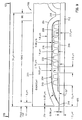
- the insulation stack 300 of the present head is compared to an insulation stack 302 of a low profile type write head and to an insulation stack 304 of a typical prior art write head.
- the present head investigated is typified by the head 200 shown in Fig. 9. It can be seen that the write coil layer 306 of the present write head is considerably closer to the ZTH than the locations of the write coils 308 and 310 of the other heads to the ZTH. This significantly decreases the lengths of the first and second pole pieces in the present write head. Further, it should be noted that the apex angles of the insulation stacks 302 and 304 are significantly greater at the ZTH than the apex angle of the insulation stack 300 of the present head. These increased apex angles will contribute to unwanted reflective notching of the second pole tip, as discussed hereinabove. Accordingly, the insulation stack 300 is considerably more favorable than the insulation stacks 302 and 304.
- Fig. 15 illustrates various levels of photoresist layers employed for frame plating the second pole piece layer of the present head and the other two heads investigated. It can be seen that the photoresist layer 320 is shallow in the pole tip region which is desirable for minimizing dispersion of light during the light exposure step of the photoresist layer. The photoresist layer 322 of the low profile head is considerably deeper in the pole tip region and the photoresist layer 324 of the prior art head 304 is still deeper in the pole tip region. Accordingly, the high aspect ratios of the insulation stacks and the thicker resist layers employed for frame plating the second pole piece for the other two heads investigated significantly increases the risk of reflective notching which degrades the track width density of the write head.
- a method of making the write head includes forming the first pole piece layer 212 in the pole tip, yoke and back regions, forming the first insulation layer 206 of a nonorganic material on the first pole piece layer 212 in the yoke region, forming an electrically conductive coil layer 202 in the yoke region, forming a second insulation layer 208 of baked photoresist on the coil layer 202, forming the write gap layer 216 on the first pole piece layer 212 in the pole tip region and, preferably, on the second insulation layer 208 in the yoke region to form the third insulation layer 210, etching the write gap layer at the back gap region, forming the second pole piece layer 214 on the third insulation layer 210 in the yoke region, on the write gap layer 216 in the pole tip region and connecting the second pole piece layer 214 to the first pole piece layer 212 in the back gap region (BG) at 218.
- BG back gap region
- the forming of the coil layer 202 and the forming of the second pole piece layer 214 forms the coil layer 202 with a thickness that is equal to or greater than the thickness of the second pole piece layer 214.
- all of the significant dimensions such as the thickness of the write gap layer 216, the zero throat height, the distance of the coil layer 202 to the ABS, the pitch of the coil, the thicknesses of the first and second pole piece layers 212 and 214, the height of the insulation stack 204 and the flare point are all scaled down proportionally. Proportional scaling has not been applied to the write coil layer 202 so as to prevent undue heating of the head.
- the write lead has a well-defined second pole tip and a write gap layer that has a reliably defined thickness at the ABS.
- the write head that is scaled down without causing a protrusion problem at the ABS.
- the write head has a lower stack height even though a thickness of a write coil layer is not scaled down proportionally with other parameters of the write head.
- the construction employed does not increase reflective notching, decreases alteration of the write gap thickness, increases the data rate and reduces protrusion at the air bearing surface.
Landscapes
- Engineering & Computer Science (AREA)
- Manufacturing & Machinery (AREA)
- Magnetic Heads (AREA)
- Adjustment Of The Magnetic Head Position Track Following On Tapes (AREA)
Claims (10)
- Tête magnétique d'écriture (200) qui comporte une surface à coussin d'air (ABS), une hauteur d'étranglement nulle (ZTH), un point d'évasement et une région de culasse qui est située entre une région de pointe polaire et une région d'entrefer arrière, la région de pointe polaire s'étendant depuis la surface ABS vers le point d'évasement et la région de culasse s'étendant depuis le point d'évasement vers la région d'entrefer arrière comprenant :des première et seconde couches de pièce polaire ferromagnétiques (212, 214) s'étendant sur toutes les régions de pointe polaire, de culasse et d'entrefer arrière, chaque couche de pièce polaire présentant une épaisseur dans la région de la culasse,une pile d'isolement (204),une couche de bobinage électriquement conductrice (202) incorporée dans la pile d'isolement, la couche de bobinage présentant une épaisseur,la pile d'isolement (204) étant située entre les première et seconde couches de pièce polaire (212, 214) dans la culasse,une couche d'entrefer d'écriture non magnétique (216) située entre les première et seconde couches de pièce polaire (212, 214) dans la région de la pointe polaire,les première et seconde couches de pièce polaire (212, 214) étant reliées ensemble dans la région d'entrefer arrière, etl'épaisseur de la couche de bobinage (202) étant supérieure ou égale à l'épaisseur de la seconde couche de pièce polaire (214),la tête d'écriture magnétique (200) étant caractérisée en ce que la pile d'isolement (204) comprend :une première couche d'isolement (206) de matériau inorganique directement sur la première couche de pièce polaire (214) dans la région de la culasse,la couche de bobinage (202) étant directement sur la première couche d'isolement (206), etune seconde couche d'isolement (208) de résine photosensible cuite directement sur la couche de bobinage (202) et qui constitue la seule couche de résine photosensible cuite dans la pile d'isolement.
- Tête magnétique d'écriture (200) selon la revendication 1, dans laquelle la pile d'isolement (204) comprend en outre :une troisième couche d'isolement directement sur la seconde couche d'isolement,la troisième couche d'isolement étant une extension de la couche d'entrefer d'écriture (216).
- Tête magnétique d'écriture (200) selon la revendication 1 ou la revendication 2, dans laquelle le matériau inorganique est sélectionné à partir du groupe de l'oxyde d'aluminium (Al2O3), du dioxyde de silicium (SiO2) et du silicium (Si).
- Tête magnétique d'écriture (200) selon l'une quelconque des revendications 1 à 3, comprenant :la première couche d'isolement (206) présentant une épaisseur d'environ 0,2 de l'épaisseur de la couche de bobinage (202),la seconde couche d'isolement (208) présentant une hauteur au-dessus de la couche de bobinage (202) d'environ 0,40 de l'épaisseur de la couche de bobinage (202), etla couche d'entrefer d'écriture (216) présentant une épaisseur d'environ 1/20 de l'épaisseur de la couche de bobinage (202).
- Tête magnétique d'écriture (200) selon l'une quelconque des revendications précédentes, comprenant :la pile d'isolement (204) présentant une hauteur d'environ le double de l'épaisseur de la couche de bobinage (202),une distance depuis la surface ABS jusqu'à la couche de bobinage (202) qui est d'environ trois fois l'épaisseur de la couche de bobinage (202), etla hauteur ZTH étant environ 1/3 de l'épaisseur de la couche de bobinage (202).
- Unité de disque magnétique qui comprend au moins une tête de lecture et une tête d'écriture combinées, dans laquelle la tête d'écriture est selon l'une quelconque des revendications 1 à 5, et la tête de lecture comprend :un capteur de lecture et des première et seconde couches de conducteur reliées au capteur de lecture,des première et seconde couches d'entrefer de lecture non magnétiques électriquement isolantes,le capteur de lecture et les première et seconde couches de conducteur étant situés entre les première et seconde couches d'entrefer de lecture,des première et seconde couches de blindage, etles première et seconde couches d'entrefer étant situées entre les première et seconde couches de blindage,l'unité de disque magnétique comprenant en outre :un boítier,un disque magnétique supporté avec possibilité de rotation dans le boítier,un support monté dans le boítier afin de supporter la tête magnétique avec sa surface ABS face au disque magnétique, de sorte que la tête magnétique soit dans une relation de transduction avec le disque magnétique,un moyen destiné à faire tourner le disque magnétique,un moyen de positionnement relié au support afin de déplacer la tête magnétique vers des positions multiples par rapport audit disque magnétique, etun moyen de traitement relié à la tête magnétique, au moyen destiné à faire tourner le disque magnétique et au moyen de positionnement afin d'échanger des signaux avec la tête magnétique incorporée, en vue de commander le déplacement du disque magnétique et en vue de commander la position de la tête magnétique.
- Procédé de réalisation d'une tête magnétique d'écriture (200) qui comporte une surface de coussin d'air (ABS), une hauteur d'étranglement nulle (ZTH), un point d'évasement et une région de culasse qui est située entre une région de pointe polaire et une région d'entrefer arrière, la région de pointe polaire s'étendant depuis la surface ABS vers le point d'évasement et la région de culasse s'étendant depuis le point d'évasement vers la région d'entrefer arrière, comprenant :la formation d'une première couche de pièce polaire ferromagnétique (212) dans les régions de pointe polaires de culasse et d'entrefer arrière,la formation d'une première couche d'isolement (206) sur la première couche de pièce polaire (212) dans la région de culasse,la formation d'une couche de bobinage électriquement conductrice (202) présentant une épaisseur sur la première couche d'isolement,la formation d'une seconde couche d'isolement (208) sur la couche de bobinage (212),la formation d'une couche d'entrefer d'écriture non magnétique (216) sur la première couche de pièce polaire (212) dans la région de pointe polaire,la formation d'une seconde couche de pièce polaire ferromagnétique (214) sur la seconde couche d'isolement (208) dans la région de la culasse, sur l'entrefer d'écriture dans la région de pointe polaire, et reliée à la première couche de pièce polaire (212) dans la région de l'entrefer arrière, etla formation de la couche de bobinage (202) et la formation de la seconde couche de pièce polaire (214) formant la couche de bobinage (202) avec une épaisseur qui est supérieure ou égale à une épaisseur de la seconde couche de pièce polaire,le procédé étant caractérisé en ce que la pile d'isolement (204) est réalisée par :la formation d'une première couche d'isolement (206) d'un matériau inorganique directement sur la première couche de pièce polaire (212) dans la région de la culasse,la formation de la couche de bobinage (202) directement sur la première couche d'isolement, etla formation d'une seconde couche d'isolement (208) de résine photosensible cuite directement sur la couche de bobinage (202) qui est la seule couche de résine photosensible cuite dans la pile d'isolement (204).
- Procédé selon la revendication 7, dans lequel la pile d'isolement (204) est en outre réalisée par :la formation d'une troisième couche d'isolement directement sur la seconde couche d'isolement, dans laquelle la troisième couche d'isolement constitue une extension de la couche d'entrefer d'écriture.
- Procédé selon la revendication 7 ou la revendication 8, comprenant :la formation de la première couche d'isolement avec une épaisseur d'environ 0,2 de l'épaisseur du bobinage,la formation de la seconde couche d'isolement avec une hauteur au-dessus de la couche de bobinage (202) d'environ 0,40 de l'épaisseur de la couche de bobinage, etla formation de la couche d'entrefer d'écriture avec une épaisseur d'environ 1/20 de l'épaisseur de la couche de bobinage.
- Procédé selon l'une quelconque des revendications 7 à 9, comprenant :la formation de la pile d'isolement (204) avec une hauteur qui est environ double de l'épaisseur de la couche de bobinage (202),la formation de la couche de bobinage (202) avec une distance depuis la surface ABS jusqu'à la couche de bobinage (202) qui est d'environ trois fois l'épaisseur de la couche de bobinage, etla formation de la hauteur ZTH avec une épaisseur d'environ 1/3 de l'épaisseur de la couche de bobinage.
Applications Claiming Priority (3)
| Application Number | Priority Date | Filing Date | Title |
|---|---|---|---|
| US09/205,476 US6181514B1 (en) | 1998-12-04 | 1998-12-04 | Scaled write head with high recording density and high data rate |
| US205476 | 1998-12-04 | ||
| PCT/GB1999/003950 WO2000034945A1 (fr) | 1998-12-04 | 1999-11-29 | Tete magnetique d'ecriture |
Publications (2)
| Publication Number | Publication Date |
|---|---|
| EP1135770A1 EP1135770A1 (fr) | 2001-09-26 |
| EP1135770B1 true EP1135770B1 (fr) | 2002-10-02 |
Family
ID=22762340
Family Applications (1)
| Application Number | Title | Priority Date | Filing Date |
|---|---|---|---|
| EP99956233A Expired - Lifetime EP1135770B1 (fr) | 1998-12-04 | 1999-11-29 | Tete magnetique d'ecriture |
Country Status (12)
| Country | Link |
|---|---|
| US (1) | US6181514B1 (fr) |
| EP (1) | EP1135770B1 (fr) |
| JP (1) | JP2002532814A (fr) |
| KR (1) | KR100420540B1 (fr) |
| CN (1) | CN1135532C (fr) |
| AT (1) | ATE225555T1 (fr) |
| AU (1) | AU1287600A (fr) |
| DE (1) | DE69903344T2 (fr) |
| HK (1) | HK1041973B (fr) |
| HU (1) | HUP0104499A3 (fr) |
| MY (1) | MY117618A (fr) |
| WO (1) | WO2000034945A1 (fr) |
Families Citing this family (32)
| Publication number | Priority date | Publication date | Assignee | Title |
|---|---|---|---|---|
| JP3799168B2 (ja) * | 1998-08-20 | 2006-07-19 | 株式会社日立グローバルストレージテクノロジーズ | 磁気記録再生装置 |
| JP2000099913A (ja) * | 1998-09-24 | 2000-04-07 | Tdk Corp | 薄膜磁気ヘッドおよびその製造方法 |
| JP3599235B2 (ja) * | 1999-07-19 | 2004-12-08 | Tdk株式会社 | 薄膜磁気ヘッド、磁気ヘッド装置及び磁気ディスク装置 |
| US6396660B1 (en) * | 1999-08-23 | 2002-05-28 | Read-Rite Corporation | Magnetic write element having a thermally dissipative structure |
| US6631546B1 (en) * | 2000-02-01 | 2003-10-14 | International Business Machines Corporation | Self-aligned void filling for mushroomed plating |
| US6493183B1 (en) * | 2000-06-29 | 2002-12-10 | International Business Machines Corporation | Thermally-assisted magnetic recording system with head having resistive heater in write gap |
| US6687083B2 (en) * | 2001-08-22 | 2004-02-03 | Hitachi Global Storage Technologies Netherlands B.V. | Enhanced low profile magnet write head |
| JP2003085707A (ja) * | 2001-09-12 | 2003-03-20 | Hitachi Ltd | 磁気ヘッドおよび磁気ヘッドの製造方法並びにこれを用いた磁気ディスク装置 |
| US6914750B2 (en) * | 2001-10-05 | 2005-07-05 | Headway Technologies, Inc. | Thermal protrusion reduction in magnet heads by utilizing heat sink layers |
| US6721138B1 (en) | 2001-10-24 | 2004-04-13 | Western Digital (Fremont), Inc. | Inductive transducer with stitched pole tip and pedestal defining zero throat height |
| JP3763526B2 (ja) * | 2002-04-04 | 2006-04-05 | Tdk株式会社 | マイクロデバイス及びその製造方法 |
| US7170713B2 (en) * | 2002-08-08 | 2007-01-30 | Hitachi Global Storage Technologies Netherlands B.V. | Heat sink for a magnetic recording head |
| EP1398763B1 (fr) * | 2002-08-08 | 2006-05-03 | Hitachi Global Storage Technologies Netherlands B.V. | Radiateur pour une tête d'enregistrement magnétique |
| US6989963B2 (en) * | 2002-09-13 | 2006-01-24 | Seagate Technology Llc | Writer core structures having improved thermal dissipation properties |
| JP3799322B2 (ja) * | 2002-11-15 | 2006-07-19 | 株式会社日立グローバルストレージテクノロジーズ | 磁気ディスク装置 |
| US6867940B2 (en) * | 2003-06-16 | 2005-03-15 | Seagate Technology Llc | Method and apparatus for mitigating thermal pole tip protrusion |
| US7268973B2 (en) * | 2003-07-24 | 2007-09-11 | Hitachi Global Storage Technologies Netherlands, B.V. | Perpendicular magnetic head having thermally assisted recording element |
| US7031121B2 (en) * | 2003-07-30 | 2006-04-18 | Hitachi Global Storage Technologies Netherlands B.V. | Perpendicular recording magnetic head with a write shield magnetically coupled to a first pole piece |
| US6975472B2 (en) * | 2003-09-12 | 2005-12-13 | Seagate Technology Llc | Head with heating element and control regime therefor |
| US7310204B1 (en) | 2003-12-19 | 2007-12-18 | Western Digital (Fremont), Llc | Inductive writer design for using a soft magnetic pedestal having a high magnetic saturation layer |
| US7748439B2 (en) | 2004-04-13 | 2010-07-06 | Headway Technologies, Inc. | Heat extractor for magnetic reader-writer |
| US7522379B1 (en) | 2004-07-30 | 2009-04-21 | Western Digital (Fremont), Llc | Write element with recessed pole and heat sink layer for ultra-high density writing |
| US7379269B1 (en) * | 2004-07-30 | 2008-05-27 | Western Digital (Fremont), Llc | Write element with reduced yoke length for ultra-high density writing |
| US7238292B1 (en) | 2004-07-30 | 2007-07-03 | Western Digital (Fremont), Inc. | Method of fabricating a write element with a reduced yoke length |
| US7411264B2 (en) * | 2004-11-18 | 2008-08-12 | Seagate Technology Llc | Etch-stop layers for patterning block structures for reducing thermal protrusion |
| JP2006268947A (ja) * | 2005-03-23 | 2006-10-05 | Fujitsu Ltd | 磁気ヘッド構造 |
| US7808746B2 (en) | 2005-08-11 | 2010-10-05 | Seagate Technology Llc | Method and apparatus for active control of spacing between a head and a storage medium |
| US8724263B2 (en) | 2005-08-11 | 2014-05-13 | Seagate Technology Llc | Method for active control of spacing between a head and a storage medium |
| US7791834B2 (en) * | 2006-08-14 | 2010-09-07 | International Business Machines Corporation | Magnetic head having a ratio of back gap width to front gap width in about a defined range |
| CN101241707A (zh) | 2007-02-07 | 2008-08-13 | 新科实业有限公司 | 具有静电防护结构的柔性装配磁头、磁头折片组合及磁盘驱动单元 |
| CN102270458A (zh) | 2010-06-03 | 2011-12-07 | 新科实业有限公司 | 具有灵敏反馈装置用于形成磁头的磁条及制造磁头的方法 |
| US8817425B1 (en) * | 2013-03-15 | 2014-08-26 | Headway Technologies, Inc. | Dual-piece heat sink layer for robust reader in magnetic recording head |
Family Cites Families (19)
| Publication number | Priority date | Publication date | Assignee | Title |
|---|---|---|---|---|
| JPS5819716A (ja) * | 1981-07-27 | 1983-02-04 | Hitachi Ltd | 薄膜磁気ヘツドおよびその製造方法 |
| JPS5898822A (ja) * | 1981-12-09 | 1983-06-11 | Comput Basic Mach Technol Res Assoc | 薄膜磁気ヘツド |
| JPS58212615A (ja) * | 1982-06-04 | 1983-12-10 | Hitachi Ltd | 薄膜磁気ヘツド |
| JPS5971115A (ja) * | 1982-10-15 | 1984-04-21 | Hitachi Ltd | 磁気ヘッド |
| JPH07118057B2 (ja) * | 1984-08-06 | 1995-12-18 | 富士写真フイルム株式会社 | 薄膜磁気ヘッドの製造方法 |
| JPS63177311A (ja) * | 1987-01-19 | 1988-07-21 | Hitachi Ltd | 薄膜磁気ヘツド |
| JPH01128215A (ja) * | 1987-11-12 | 1989-05-19 | Sumitomo Metal Ind Ltd | 薄膜磁気ヘッドおよびその製造方法 |
| JPH0294013A (ja) * | 1988-09-30 | 1990-04-04 | Hitachi Ltd | 薄膜磁気ヘツド |
| US5032944A (en) * | 1989-01-12 | 1991-07-16 | Mitsubishi Denki Kabushiki Kaisha | Membrane type magnetic head |
| US5241440A (en) * | 1989-08-23 | 1993-08-31 | Hitachi, Ltd. | Thin film magnetic head and manufacturing method therefor |
| DE69123487T2 (de) * | 1990-05-31 | 1997-06-26 | Sony Corp | Dünnfilmmagnetkopf |
| JPH05151534A (ja) * | 1991-11-29 | 1993-06-18 | Hitachi Ltd | 複合型薄膜磁気ヘツド |
| JPH0778312A (ja) * | 1993-09-09 | 1995-03-20 | Tdk Corp | 薄膜磁気ヘッド |
| US5486968A (en) * | 1993-11-10 | 1996-01-23 | International Business Machines Corporation | Method and apparatus for simultaneous write head planarization and lead routing |
| TW273618B (fr) * | 1994-08-25 | 1996-04-01 | Ibm | |
| JPH08138211A (ja) * | 1994-11-10 | 1996-05-31 | Fujitsu Ltd | 薄膜磁気ヘッド |
| US5606478A (en) * | 1994-12-08 | 1997-02-25 | International Business Machines Corporation | Ni45 Fe55 metal-in-gap thin film magnetic head |
| US5515221A (en) * | 1994-12-30 | 1996-05-07 | International Business Machines Corporation | Magnetically stable shields for MR head |
| US5798897A (en) | 1996-10-21 | 1998-08-25 | International Business Machines Corporation | Inductive write head with insulation stack configured for eliminating reflective notching |
-
1998
- 1998-12-04 US US09/205,476 patent/US6181514B1/en not_active Expired - Lifetime
-
1999
- 1999-11-16 MY MYPI99004975A patent/MY117618A/en unknown
- 1999-11-29 EP EP99956233A patent/EP1135770B1/fr not_active Expired - Lifetime
- 1999-11-29 KR KR10-2001-7006777A patent/KR100420540B1/ko not_active Expired - Fee Related
- 1999-11-29 CN CNB998141011A patent/CN1135532C/zh not_active Expired - Fee Related
- 1999-11-29 AT AT99956233T patent/ATE225555T1/de not_active IP Right Cessation
- 1999-11-29 JP JP2000587326A patent/JP2002532814A/ja active Pending
- 1999-11-29 AU AU12876/00A patent/AU1287600A/en not_active Abandoned
- 1999-11-29 HK HK02103372.0A patent/HK1041973B/zh not_active IP Right Cessation
- 1999-11-29 WO PCT/GB1999/003950 patent/WO2000034945A1/fr not_active Ceased
- 1999-11-29 DE DE69903344T patent/DE69903344T2/de not_active Expired - Fee Related
- 1999-11-29 HU HU0104499A patent/HUP0104499A3/hu unknown
Also Published As
| Publication number | Publication date |
|---|---|
| DE69903344D1 (de) | 2002-11-07 |
| HUP0104499A3 (en) | 2002-06-28 |
| AU1287600A (en) | 2000-06-26 |
| WO2000034945A1 (fr) | 2000-06-15 |
| CN1329740A (zh) | 2002-01-02 |
| EP1135770A1 (fr) | 2001-09-26 |
| HK1041973B (zh) | 2004-09-10 |
| ATE225555T1 (de) | 2002-10-15 |
| HK1041973A1 (en) | 2002-07-26 |
| CN1135532C (zh) | 2004-01-21 |
| KR20010101098A (ko) | 2001-11-14 |
| JP2002532814A (ja) | 2002-10-02 |
| HUP0104499A2 (hu) | 2002-03-28 |
| DE69903344T2 (de) | 2003-07-31 |
| MY117618A (en) | 2004-07-31 |
| US6181514B1 (en) | 2001-01-30 |
| KR100420540B1 (ko) | 2004-03-02 |
Similar Documents
| Publication | Publication Date | Title |
|---|---|---|
| EP1135770B1 (fr) | Tete magnetique d'ecriture | |
| US6552874B1 (en) | Shared pole magnetic read-write head for achieving optimized erase band width and method of fabricating the same | |
| US6339523B1 (en) | Write head before read head constructed magnetic head with track width and zero throat height defined by first pole tip | |
| US6693769B2 (en) | High data rate write head | |
| US6377423B2 (en) | Planar stitched write head having write coil insulated with inorganic insulation | |
| US6417998B1 (en) | Ultra small advanced write transducer and method for making same | |
| EP0389143B1 (fr) | Têtes magnétiques à films minces, leur fabrication et appareil de stockage d'information magnétique les incluant | |
| US5935644A (en) | Method of making thin film induction recording head having an inset first insulation layer that defines zero throat height and pole tip apex angle | |
| US6353511B1 (en) | Thin film write head for improved high speed and high density recording | |
| US6278591B1 (en) | Inverted merged MR head having plated notched first pole tip and self-aligned second pole tip | |
| US7464458B2 (en) | Method for manufacturing a self-aligned, notched trailing shield for perpendicular recording | |
| US6104576A (en) | Inductive head with reduced height insulation stack due to partial coverage zero throat height defining insulation layer | |
| US6785953B2 (en) | Process of fabricating a write head with protection of a second pole tip thickness | |
| KR19980032173A (ko) | 제로 스롯 높이를 정하는 절연층의 평탄부 상에서 리세스되고 스티치된 요크를 갖는 기록 헤드 | |
| US6862798B2 (en) | Method of making a narrow pole tip by ion beam deposition | |
| US6687083B2 (en) | Enhanced low profile magnet write head | |
| US6722018B2 (en) | Method of forming a second pole piece of a write head | |
| US6725527B2 (en) | Method of making a magnetic head assembly having open yoke write head with highly defined narrow track width | |
| US5296979A (en) | Magnetic disc apparatus with thin film head suitable for high-density recording | |
| US20050068677A1 (en) | Stitched write head with staircase P2 defined throat height | |
| US7969683B2 (en) | Write first design for a perpendicular thin film head | |
| US7002776B2 (en) | Thin film magnetic head and method of manufacturing same | |
| MXPA01005359A (en) | Magnetic write head |
Legal Events
| Date | Code | Title | Description |
|---|---|---|---|
| PUAI | Public reference made under article 153(3) epc to a published international application that has entered the european phase |
Free format text: ORIGINAL CODE: 0009012 |
|
| 17P | Request for examination filed |
Effective date: 20010622 |
|
| AK | Designated contracting states |
Kind code of ref document: A1 Designated state(s): AT BE CH CY DE DK ES FI FR GB GR IE IT LI LU MC NL PT SE |
|
| GRAG | Despatch of communication of intention to grant |
Free format text: ORIGINAL CODE: EPIDOS AGRA |
|
| 17Q | First examination report despatched |
Effective date: 20020131 |
|
| GRAG | Despatch of communication of intention to grant |
Free format text: ORIGINAL CODE: EPIDOS AGRA |
|
| GRAH | Despatch of communication of intention to grant a patent |
Free format text: ORIGINAL CODE: EPIDOS IGRA |
|
| GRAH | Despatch of communication of intention to grant a patent |
Free format text: ORIGINAL CODE: EPIDOS IGRA |
|
| GRAA | (expected) grant |
Free format text: ORIGINAL CODE: 0009210 |
|
| AK | Designated contracting states |
Kind code of ref document: B1 Designated state(s): AT BE CH CY DE DK ES FI FR GB GR IE IT LI LU MC NL PT SE |
|
| PG25 | Lapsed in a contracting state [announced via postgrant information from national office to epo] |
Ref country code: NL Free format text: LAPSE BECAUSE OF FAILURE TO SUBMIT A TRANSLATION OF THE DESCRIPTION OR TO PAY THE FEE WITHIN THE PRESCRIBED TIME-LIMIT Effective date: 20021002 Ref country code: LI Free format text: LAPSE BECAUSE OF FAILURE TO SUBMIT A TRANSLATION OF THE DESCRIPTION OR TO PAY THE FEE WITHIN THE PRESCRIBED TIME-LIMIT Effective date: 20021002 Ref country code: IT Free format text: LAPSE BECAUSE OF FAILURE TO SUBMIT A TRANSLATION OF THE DESCRIPTION OR TO PAY THE FEE WITHIN THE PRE;WARNING: LAPSES OF ITALIAN PATENTS WITH EFFECTIVE DATE BEFORE 2007 MAY HAVE OCCURRED AT ANY TIME BEFORE 2007. THE CORRECT EFFECTIVE DATE MAY BE DIFFERENT FROM THE ONE RECORDED.SCRIBED TIME-LIMIT Effective date: 20021002 Ref country code: GR Free format text: LAPSE BECAUSE OF FAILURE TO SUBMIT A TRANSLATION OF THE DESCRIPTION OR TO PAY THE FEE WITHIN THE PRESCRIBED TIME-LIMIT Effective date: 20021002 Ref country code: FI Free format text: LAPSE BECAUSE OF FAILURE TO SUBMIT A TRANSLATION OF THE DESCRIPTION OR TO PAY THE FEE WITHIN THE PRESCRIBED TIME-LIMIT Effective date: 20021002 Ref country code: CH Free format text: LAPSE BECAUSE OF FAILURE TO SUBMIT A TRANSLATION OF THE DESCRIPTION OR TO PAY THE FEE WITHIN THE PRESCRIBED TIME-LIMIT Effective date: 20021002 Ref country code: BE Free format text: LAPSE BECAUSE OF FAILURE TO SUBMIT A TRANSLATION OF THE DESCRIPTION OR TO PAY THE FEE WITHIN THE PRESCRIBED TIME-LIMIT Effective date: 20021002 Ref country code: AT Free format text: LAPSE BECAUSE OF FAILURE TO SUBMIT A TRANSLATION OF THE DESCRIPTION OR TO PAY THE FEE WITHIN THE PRESCRIBED TIME-LIMIT Effective date: 20021002 |
|
| REF | Corresponds to: |
Ref document number: 225555 Country of ref document: AT Date of ref document: 20021015 Kind code of ref document: T |
|
| REG | Reference to a national code |
Ref country code: GB Ref legal event code: FG4D |
|
| REG | Reference to a national code |
Ref country code: CH Ref legal event code: EP |
|
| REG | Reference to a national code |
Ref country code: IE Ref legal event code: FG4D |
|
| REG | Reference to a national code |
Ref country code: CH Ref legal event code: NV Representative=s name: JULIAN DAVID WILLIAMS C/O INTERNATIONAL BUSINESS M |
|
| REF | Corresponds to: |
Ref document number: 69903344 Country of ref document: DE Date of ref document: 20021107 |
|
| PG25 | Lapsed in a contracting state [announced via postgrant information from national office to epo] |
Ref country code: LU Free format text: LAPSE BECAUSE OF NON-PAYMENT OF DUE FEES Effective date: 20021129 |
|
| PG25 | Lapsed in a contracting state [announced via postgrant information from national office to epo] |
Ref country code: CY Free format text: LAPSE BECAUSE OF FAILURE TO SUBMIT A TRANSLATION OF THE DESCRIPTION OR TO PAY THE FEE WITHIN THE PRESCRIBED TIME-LIMIT Effective date: 20021130 |
|
| PG25 | Lapsed in a contracting state [announced via postgrant information from national office to epo] |
Ref country code: SE Free format text: LAPSE BECAUSE OF FAILURE TO SUBMIT A TRANSLATION OF THE DESCRIPTION OR TO PAY THE FEE WITHIN THE PRESCRIBED TIME-LIMIT Effective date: 20030102 Ref country code: PT Free format text: LAPSE BECAUSE OF FAILURE TO SUBMIT A TRANSLATION OF THE DESCRIPTION OR TO PAY THE FEE WITHIN THE PRESCRIBED TIME-LIMIT Effective date: 20030102 Ref country code: DK Free format text: LAPSE BECAUSE OF FAILURE TO SUBMIT A TRANSLATION OF THE DESCRIPTION OR TO PAY THE FEE WITHIN THE PRESCRIBED TIME-LIMIT Effective date: 20030102 |
|
| NLV1 | Nl: lapsed or annulled due to failure to fulfill the requirements of art. 29p and 29m of the patents act | ||
| ET | Fr: translation filed | ||
| PG25 | Lapsed in a contracting state [announced via postgrant information from national office to epo] |
Ref country code: ES Free format text: LAPSE BECAUSE OF FAILURE TO SUBMIT A TRANSLATION OF THE DESCRIPTION OR TO PAY THE FEE WITHIN THE PRESCRIBED TIME-LIMIT Effective date: 20030429 |
|
| REG | Reference to a national code |
Ref country code: CH Ref legal event code: PL |
|
| PG25 | Lapsed in a contracting state [announced via postgrant information from national office to epo] |
Ref country code: MC Free format text: LAPSE BECAUSE OF NON-PAYMENT OF DUE FEES Effective date: 20030601 |
|
| PLBE | No opposition filed within time limit |
Free format text: ORIGINAL CODE: 0009261 |
|
| STAA | Information on the status of an ep patent application or granted ep patent |
Free format text: STATUS: NO OPPOSITION FILED WITHIN TIME LIMIT |
|
| 26N | No opposition filed |
Effective date: 20030703 |
|
| REG | Reference to a national code |
Ref country code: GB Ref legal event code: 732E |
|
| REG | Reference to a national code |
Ref country code: FR Ref legal event code: TP |
|
| PGFP | Annual fee paid to national office [announced via postgrant information from national office to epo] |
Ref country code: IE Payment date: 20080923 Year of fee payment: 10 |
|
| PGFP | Annual fee paid to national office [announced via postgrant information from national office to epo] |
Ref country code: DE Payment date: 20081126 Year of fee payment: 10 |
|
| PGFP | Annual fee paid to national office [announced via postgrant information from national office to epo] |
Ref country code: FR Payment date: 20081017 Year of fee payment: 10 |
|
| PGFP | Annual fee paid to national office [announced via postgrant information from national office to epo] |
Ref country code: GB Payment date: 20081021 Year of fee payment: 10 |
|
| GBPC | Gb: european patent ceased through non-payment of renewal fee |
Effective date: 20091129 |
|
| REG | Reference to a national code |
Ref country code: FR Ref legal event code: ST Effective date: 20100730 |
|
| REG | Reference to a national code |
Ref country code: IE Ref legal event code: MM4A |
|
| PG25 | Lapsed in a contracting state [announced via postgrant information from national office to epo] |
Ref country code: IE Free format text: LAPSE BECAUSE OF NON-PAYMENT OF DUE FEES Effective date: 20091130 Ref country code: FR Free format text: LAPSE BECAUSE OF NON-PAYMENT OF DUE FEES Effective date: 20091130 |
|
| PG25 | Lapsed in a contracting state [announced via postgrant information from national office to epo] |
Ref country code: DE Free format text: LAPSE BECAUSE OF NON-PAYMENT OF DUE FEES Effective date: 20100601 |
|
| PG25 | Lapsed in a contracting state [announced via postgrant information from national office to epo] |
Ref country code: GB Free format text: LAPSE BECAUSE OF NON-PAYMENT OF DUE FEES Effective date: 20091129 |