EP1139122A2 - Integriert optischer Baustein mit fester dreidimensionaler Struktur - Google Patents
Integriert optischer Baustein mit fester dreidimensionaler Struktur Download PDFInfo
- Publication number
- EP1139122A2 EP1139122A2 EP01107915A EP01107915A EP1139122A2 EP 1139122 A2 EP1139122 A2 EP 1139122A2 EP 01107915 A EP01107915 A EP 01107915A EP 01107915 A EP01107915 A EP 01107915A EP 1139122 A2 EP1139122 A2 EP 1139122A2
- Authority
- EP
- European Patent Office
- Prior art keywords
- light
- semiconductor crystal
- ball
- emitting
- receiving
- Prior art date
- Legal status (The legal status is an assumption and is not a legal conclusion. Google has not performed a legal analysis and makes no representation as to the accuracy of the status listed.)
- Withdrawn
Links
Images


Classifications
-
- G—PHYSICS
- G02—OPTICS
- G02B—OPTICAL ELEMENTS, SYSTEMS OR APPARATUS
- G02B6/00—Light guides; Structural details of arrangements comprising light guides and other optical elements, e.g. couplings
- G02B6/10—Light guides; Structural details of arrangements comprising light guides and other optical elements, e.g. couplings of the optical waveguide type
- G02B6/12—Light guides; Structural details of arrangements comprising light guides and other optical elements, e.g. couplings of the optical waveguide type of the integrated circuit kind
- G02B6/12004—Combinations of two or more optical elements
-
- G—PHYSICS
- G02—OPTICS
- G02B—OPTICAL ELEMENTS, SYSTEMS OR APPARATUS
- G02B6/00—Light guides; Structural details of arrangements comprising light guides and other optical elements, e.g. couplings
- G02B6/10—Light guides; Structural details of arrangements comprising light guides and other optical elements, e.g. couplings of the optical waveguide type
- G02B6/12—Light guides; Structural details of arrangements comprising light guides and other optical elements, e.g. couplings of the optical waveguide type of the integrated circuit kind
- G02B6/12002—Three-dimensional structures
-
- G—PHYSICS
- G02—OPTICS
- G02B—OPTICAL ELEMENTS, SYSTEMS OR APPARATUS
- G02B6/00—Light guides; Structural details of arrangements comprising light guides and other optical elements, e.g. couplings
- G02B6/10—Light guides; Structural details of arrangements comprising light guides and other optical elements, e.g. couplings of the optical waveguide type
- G02B6/12—Light guides; Structural details of arrangements comprising light guides and other optical elements, e.g. couplings of the optical waveguide type of the integrated circuit kind
- G02B6/13—Integrated optical circuits characterised by the manufacturing method
- G02B6/132—Integrated optical circuits characterised by the manufacturing method by deposition of thin films
-
- G—PHYSICS
- G02—OPTICS
- G02B—OPTICAL ELEMENTS, SYSTEMS OR APPARATUS
- G02B6/00—Light guides; Structural details of arrangements comprising light guides and other optical elements, e.g. couplings
- G02B6/10—Light guides; Structural details of arrangements comprising light guides and other optical elements, e.g. couplings of the optical waveguide type
- G02B6/12—Light guides; Structural details of arrangements comprising light guides and other optical elements, e.g. couplings of the optical waveguide type of the integrated circuit kind
- G02B2006/12035—Materials
- G02B2006/12061—Silicon
-
- G—PHYSICS
- G02—OPTICS
- G02B—OPTICAL ELEMENTS, SYSTEMS OR APPARATUS
- G02B6/00—Light guides; Structural details of arrangements comprising light guides and other optical elements, e.g. couplings
- G02B6/10—Light guides; Structural details of arrangements comprising light guides and other optical elements, e.g. couplings of the optical waveguide type
- G02B6/12—Light guides; Structural details of arrangements comprising light guides and other optical elements, e.g. couplings of the optical waveguide type of the integrated circuit kind
- G02B2006/12083—Constructional arrangements
- G02B2006/12121—Laser
-
- G—PHYSICS
- G02—OPTICS
- G02B—OPTICAL ELEMENTS, SYSTEMS OR APPARATUS
- G02B6/00—Light guides; Structural details of arrangements comprising light guides and other optical elements, e.g. couplings
- G02B6/10—Light guides; Structural details of arrangements comprising light guides and other optical elements, e.g. couplings of the optical waveguide type
- G02B6/12—Light guides; Structural details of arrangements comprising light guides and other optical elements, e.g. couplings of the optical waveguide type of the integrated circuit kind
- G02B2006/12083—Constructional arrangements
- G02B2006/12123—Diode
Definitions
- This method aims to solve the pin-bottle-neck problem by replacing a portion of the electric wiring by optical wiring.
- the total number of electric wires can be reduced owing to characteristics of non-electromagnetic induction and broad band of the optical wiring.
- the optical wiring is arranged using conventional optical fiber and semiconductor waveguides, the width of the optical path becomes far thicker than that of electric wires. Accordingly, only a limited portion of the electric wiring can be replaced by optical wiring, and the resultant configuration inevitably lacks flexibility.
- the above requirements are typically satisfied by a structure in which the light-emitting device is composed of III - V N semiconductor material, and the light-receiving device is composed of III-V N semiconductor material or SiGe.
- x is approximately equal to 0.03
- an active layer composed thereof can emit light at a wavelength of about 1.3 ⁇ m which cannot be absorbed by Si.
- LED light emitting diodes
- VCSEL vertical cavity surface emitting laser
- Crystal growth of the optical device will be described.
- Such technology as that disclosed in Japanese Patent Application Laid-Open No. 12(2000)-332229 can be used for the crystal growth of the optical device.
- a mask for selective growth is formed on a Si wafer with a (100) face, on which the electronic device is formed.
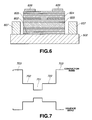
- N-type GaAs/AlAs reflective layer 602 with a reflectivity of 90 %, GaInNAs/GaAs single quantum well (SQW) active layer 603, and p-type GaAs/AlAs reflective layer 604 with a reflectivity of 90 % are formed on the wafer of the buffer layer 502.
- reflective layers 602 and 604 are provided to enhance its emission efficiency (i.e., to effectively take out much light in a desired direction).
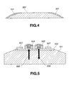
- the Si ball 101 is entirely covered with a nitride layer or the like, and a flat portion for forming an optical device thereon with a size of about 10 ⁇ m is formed by abrasion and chemical polishing.
- the (001) face and its equivalent faces (in total, six faces) are used (see Fig. 8).
- the (111) face and its equivalent faces can also be used.
- the combination of AlNAs/GaNAs is used in the n-type reflective layer 602 to achieve the lattice matching between the reflective layer 602 and the GaNAs buffer layer 502, and reduce the hetero-barrier in a conduction band of the reflective layer 604.
- a highly-reflective layer can be formed with a small number of layers, and at the same time a series resistance due to the hetero-barrier can be reduced.
- VCSEL 801 capable of operating at small current and low voltage can be achieved.
- the active layer 603 is formed of III - V N and III - V semiconductor materials to obtain the radiation wavelength (e.g., 1.3 ⁇ m) longer than a wavelength of Si absorption edge such that the interior of the Si ball 101 can be used as an optical transmission line and achieve a large band-offset in the conduction band such that thermal characteristics of the VCSEL can be improved.
- the radiation wavelength e.g., 1.3 ⁇ m
- the light-receiving device can also be fabricated by a method similar to the above fabrication method of the light source. Those optical devices can be fabricated at a time by the above selective growth technique (see Fig. 9), but the devices can be separately fabricated by the selective growth. Fig. 8 illustrates the latter example.
- the active layer of the VCSEL 801 needs to be formed of III-V N and III-V semiconductor materials such that the interior of the Si ball 101 can be used as an optical transmission line, but the active layer of the light-receiving device 802 may be formed of SiGe such that light at a 1.3- ⁇ m band can be received thereby.
- the active layer of the light-receiving device 802 is formed of SiGe, selective growths for the light source and the light-receiving device need to be separately performed.
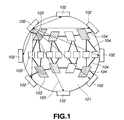
- a processor element (PE) 103 consisting of CMOS and the like
- necessary processing is performed in the PE 103.
- its output is supplied to another PE 103 through the electric wire 104 or optical path 105.
- the electric wire 104 transmits the signal in the same way as an ordinary IC.
- the optical directivity factor of the laser used in the second embodiment is high, and hence, the signal is transmitted only to a desired light-receiving device. For example, an optical signal emitted from the (001) face can be received only by the light-receiving device 102 on the (00-1) face as illustrated in Fig. 8.
- an optical signal emitted from the (100) face can be received only by the light-receiving device 102 on the (-100) face.
- the received signal is processed by the PE nearby, and transmitted through the electric wire 104 or optical wiring 105.
- electric wiring 104 and optical wiring 105 can be organically connected.
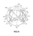
- Fig. 10 illustrates the third embodiment.
- reference numeral 102a is a light-emitting device for 1 ⁇ N optical wiring.
- an output from the PE can be converted into multiple outputs (i.e., fan-out).
- Reference numeral 102b is a light-emitting device for 1 ⁇ 1 optical wiring.
- 1 ⁇ 1 optical wiring can be achieved. In the 1 ⁇ 1 optical wiring, high speed data transfer can be achieved though flexibility of the wiring is somewhat lowered compared to the 1 ⁇ N optical wiring.
- an optical device whose consumption electric power is very small can be fabricated, since a light radiation layer of GaAsN series can be readily laid down on the Si ball.
Landscapes
- Physics & Mathematics (AREA)
- Engineering & Computer Science (AREA)
- Microelectronics & Electronic Packaging (AREA)
- General Physics & Mathematics (AREA)
- Optics & Photonics (AREA)
- Light Receiving Elements (AREA)
- Semiconductor Lasers (AREA)
- Led Devices (AREA)
- Photo Coupler, Interrupter, Optical-To-Optical Conversion Devices (AREA)
- Led Device Packages (AREA)
Applications Claiming Priority (2)
| Application Number | Priority Date | Filing Date | Title |
|---|---|---|---|
| JP2000090826A JP3689615B2 (ja) | 2000-03-29 | 2000-03-29 | 立体形状を有する光電融合デバイス |
| JP2000090826 | 2000-03-29 |
Publications (2)
| Publication Number | Publication Date |
|---|---|
| EP1139122A2 true EP1139122A2 (de) | 2001-10-04 |
| EP1139122A3 EP1139122A3 (de) | 2005-01-12 |
Family
ID=18606377
Family Applications (1)
| Application Number | Title | Priority Date | Filing Date |
|---|---|---|---|
| EP01107915A Withdrawn EP1139122A3 (de) | 2000-03-29 | 2001-03-28 | Integriert optischer Baustein mit fester dreidimensionaler Struktur |
Country Status (3)
| Country | Link |
|---|---|
| US (1) | US6563137B2 (de) |
| EP (1) | EP1139122A3 (de) |
| JP (1) | JP3689615B2 (de) |
Cited By (3)
| Publication number | Priority date | Publication date | Assignee | Title |
|---|---|---|---|---|
| EP1219994A3 (de) * | 2000-12-28 | 2004-11-10 | Canon Kabushiki Kaisha | Halbleiteranordnung, optoelektronische Platte und Verfahren zu deren Herstellung |
| US6819813B2 (en) | 2002-09-11 | 2004-11-16 | International Business Machines Corporation | Optical land grid array interposer |
| EP1496381A3 (de) * | 2003-07-01 | 2008-02-06 | Matsushita Electric Industrial Co., Ltd. | Halterungsanordnung, optische Übertragungsleitung und photoelektrische Leiterplatte |
Families Citing this family (16)
| Publication number | Priority date | Publication date | Assignee | Title |
|---|---|---|---|---|
| JP3890999B2 (ja) * | 2002-02-14 | 2007-03-07 | 住友電気工業株式会社 | 光送信モジュール |
| JP3927883B2 (ja) | 2002-08-02 | 2007-06-13 | キヤノン株式会社 | 光導波装置、およびそれを用いた光電融合基板 |
| JP3897688B2 (ja) * | 2002-12-11 | 2007-03-28 | キヤノン株式会社 | 光電融合配線基板 |
| CN101853889B (zh) * | 2003-12-01 | 2012-07-04 | 加利福尼亚大学董事会 | 用于光伏器件的多频带半导体组合物 |
| US7928424B2 (en) * | 2004-03-11 | 2011-04-19 | Epistar Corporation | Nitride-based light-emitting device |
| US8562738B2 (en) | 2004-03-11 | 2013-10-22 | Epistar Corporation | Nitride-based light-emitting device |
| US9524869B2 (en) | 2004-03-11 | 2016-12-20 | Epistar Corporation | Nitride-based semiconductor light-emitting device |
| JP4019284B2 (ja) * | 2005-02-04 | 2007-12-12 | セイコーエプソン株式会社 | 面発光型装置及びその製造方法 |
| JP4019285B2 (ja) * | 2005-02-04 | 2007-12-12 | セイコーエプソン株式会社 | 面発光型装置及びその製造方法 |
| US8338186B2 (en) * | 2005-05-18 | 2012-12-25 | Ecovu Analytics Inc. | Method and system for fluid purification and analysis |
| CA2547489C (en) * | 2005-05-18 | 2011-06-14 | Ecovu Analytics Inc. | Fluid contamination analyzer and sample cell therefor |
| US20070082505A1 (en) * | 2005-10-11 | 2007-04-12 | Freescale Semiconductor, Inc. | Method of forming an electrically insulating layer on a compound semiconductor |
| US7531371B2 (en) * | 2006-02-21 | 2009-05-12 | Rather John D G | Multisurfaced microdevice system array and a method of producing the array |
| JP2007234724A (ja) * | 2006-02-28 | 2007-09-13 | Canon Inc | 垂直共振器型面発光レーザ、該垂直共振器型面発光レーザにおける二次元フォトニック結晶の製造方法 |
| JP4973940B2 (ja) * | 2007-10-15 | 2012-07-11 | ソニー株式会社 | 半導体発光素子の製造方法 |
| JP4215812B1 (ja) | 2008-02-27 | 2009-01-28 | 国立大学法人広島大学 | 光集積回路装置 |
Family Cites Families (11)
| Publication number | Priority date | Publication date | Assignee | Title |
|---|---|---|---|---|
| US5200631A (en) * | 1991-08-06 | 1993-04-06 | International Business Machines Corporation | High speed optical interconnect |
| JP3194503B2 (ja) | 1992-06-04 | 2001-07-30 | キヤノン株式会社 | 化合物半導体装置及びその製造方法 |
| US5937274A (en) * | 1995-01-31 | 1999-08-10 | Hitachi, Ltd. | Fabrication method for AlGaIn NPAsSb based devices |
| US5955776A (en) * | 1996-12-04 | 1999-09-21 | Ball Semiconductor, Inc. | Spherical shaped semiconductor integrated circuit |
| US6097472A (en) | 1997-04-17 | 2000-08-01 | Canon Kabushiki Kaisha | Apparatus and method for exposing a pattern on a ball-like device material |
| JPH1154406A (ja) | 1997-08-04 | 1999-02-26 | Mitsui High Tec Inc | 球状icの露光方法 |
| JPH11161766A (ja) * | 1997-11-28 | 1999-06-18 | Mitsui High Tec Inc | Icカード |
| US6052517A (en) * | 1998-06-30 | 2000-04-18 | Ball Semiconductor, Inc. | Spherical cell design for VLSI circuit design on a spherical semiconductor |
| JP3865944B2 (ja) * | 1998-07-23 | 2007-01-10 | Ntn株式会社 | シリコン球の製造方法および装置 |
| JP4054480B2 (ja) | 1999-05-18 | 2008-02-27 | キヤノン株式会社 | Si基板上の光電融合デバイス構造、その製造方法、及び成膜方法 |
| US6423974B1 (en) * | 1999-05-28 | 2002-07-23 | Ball Semiconductor, Inc. | X-ray imaging apparatus using spherical semiconductor detectors |
-
2000
- 2000-03-29 JP JP2000090826A patent/JP3689615B2/ja not_active Expired - Fee Related
-
2001
- 2001-03-27 US US09/817,344 patent/US6563137B2/en not_active Expired - Fee Related
- 2001-03-28 EP EP01107915A patent/EP1139122A3/de not_active Withdrawn
Cited By (6)
| Publication number | Priority date | Publication date | Assignee | Title |
|---|---|---|---|---|
| EP1219994A3 (de) * | 2000-12-28 | 2004-11-10 | Canon Kabushiki Kaisha | Halbleiteranordnung, optoelektronische Platte und Verfahren zu deren Herstellung |
| US6897430B2 (en) | 2000-12-28 | 2005-05-24 | Canon Kabushiki Kaisha | Semiconductor device, optoelectronic board, and production methods therefor |
| US6936808B2 (en) | 2000-12-28 | 2005-08-30 | Canon Kabushiki Kaisha | Semiconductor device, optoelectronic board, and production methods therefor |
| US7141778B2 (en) | 2000-12-28 | 2006-11-28 | Canon Kabushiki Kaisha | Semiconductor device, optoelectronic board, and production methods therefor |
| US6819813B2 (en) | 2002-09-11 | 2004-11-16 | International Business Machines Corporation | Optical land grid array interposer |
| EP1496381A3 (de) * | 2003-07-01 | 2008-02-06 | Matsushita Electric Industrial Co., Ltd. | Halterungsanordnung, optische Übertragungsleitung und photoelektrische Leiterplatte |
Also Published As
| Publication number | Publication date |
|---|---|
| JP3689615B2 (ja) | 2005-08-31 |
| US20010032984A1 (en) | 2001-10-25 |
| EP1139122A3 (de) | 2005-01-12 |
| US6563137B2 (en) | 2003-05-13 |
| JP2001284635A (ja) | 2001-10-12 |
Similar Documents
| Publication | Publication Date | Title |
|---|---|---|
| US6563137B2 (en) | Optoelectric integrated device having a three-dimensional solid configuration | |
| US5357122A (en) | Three-dimensional optical-electronic integrated circuit device with raised sections | |
| US5633527A (en) | Unitary lens semiconductor device | |
| US5861636A (en) | Surface emitting visible light emiting diode having ring-shaped electrode | |
| Delbeke et al. | High-efficiency semiconductor resonant-cavity light-emitting diodes: a review | |
| US6261859B1 (en) | Method for fabricating surface-emitting semiconductor device, surface-emitting semiconductor device fabricated by the method, and display device using the device | |
| US7787511B2 (en) | Array of surface-emitting laser diodes having reduced device resistance and capable of performing high output operation and method of fabricating the surface-emitting laser diode | |
| US7680162B2 (en) | Long wavelength vertical cavity surface emitting laser device and method of fabricating the same | |
| EP1026798B1 (de) | Oberflächenemittierender laser mit vertikalem Resonator (VCSEL) unter Verwendung von vergrabenen Bragg-Reflektoren und Herstellungsverfahren | |
| US20060001117A1 (en) | Semiconductor device, optoelectronic board, and production methods therefor | |
| US5665985A (en) | Light-emitting diode of edge-emitting type, light-receiving device of lateral-surface-receiving type, and arrayed light source | |
| CN104769467A (zh) | 半导体装置 | |
| CN1079076A (zh) | 竖直腔面发射激光器光学互连工艺 | |
| JPH0555703A (ja) | 面発光レーザ装置 | |
| US20240332901A1 (en) | Surface-emitting semiconductor laser and method for producing a surface-emitting semiconductor laser | |
| US20230352910A1 (en) | Light emitting element, light emitting element unit, electronic device, light emitting device, sensing device, and communication device | |
| KR100413708B1 (ko) | 광자리사이클링을지닌마이크로공동발광다이오드 | |
| JP7593332B2 (ja) | 発光素子及びその製造方法、並びに、発光素子アレイ | |
| US7406112B2 (en) | Surface-emitting laser, method for manufacturing surface-emitting laser, device and electronic apparatus | |
| US20250038478A1 (en) | Surface-emitting photonic crystal laser, optoelectronic system, and method for producing a surface-emitting photonic crystal laser | |
| US20090129426A1 (en) | Semiconductor System Having a Ring Laser Fabricated by Epitaxial Layer Overgrowth | |
| US7629187B2 (en) | Fabrication method of semiconductor luminescent device | |
| JPH03236276A (ja) | 光機能素子 | |
| JP2004063634A (ja) | 半導体分布ブラッグ反射器および面発光レーザ素子および面発光レーザアレイおよび光通信システムおよび光インターコネクションシステム | |
| JP2002252418A (ja) | 光通信システム |
Legal Events
| Date | Code | Title | Description |
|---|---|---|---|
| PUAI | Public reference made under article 153(3) epc to a published international application that has entered the european phase |
Free format text: ORIGINAL CODE: 0009012 |
|
| AK | Designated contracting states |
Kind code of ref document: A2 Designated state(s): AT BE CH CY DE DK ES FI FR GB GR IE IT LI LU MC NL PT SE TR |
|
| AX | Request for extension of the european patent |
Free format text: AL;LT;LV;MK;RO;SI |
|
| PUAL | Search report despatched |
Free format text: ORIGINAL CODE: 0009013 |
|
| AK | Designated contracting states |
Kind code of ref document: A3 Designated state(s): AT BE CH CY DE DK ES FI FR GB GR IE IT LI LU MC NL PT SE TR |
|
| AX | Request for extension of the european patent |
Extension state: AL LT LV MK RO SI |
|
| 17P | Request for examination filed |
Effective date: 20050711 |
|
| AKX | Designation fees paid |
Designated state(s): DE FR GB |
|
| STAA | Information on the status of an ep patent application or granted ep patent |
Free format text: STATUS: THE APPLICATION HAS BEEN WITHDRAWN |
|
| 18W | Application withdrawn |
Effective date: 20101015 |