EP1139392A2 - Verbesserter Träger für Waferbehälter und Verfahren zum Beladen von zwei Waferbehältern - Google Patents
Verbesserter Träger für Waferbehälter und Verfahren zum Beladen von zwei Waferbehältern Download PDFInfo
- Publication number
- EP1139392A2 EP1139392A2 EP01107075A EP01107075A EP1139392A2 EP 1139392 A2 EP1139392 A2 EP 1139392A2 EP 01107075 A EP01107075 A EP 01107075A EP 01107075 A EP01107075 A EP 01107075A EP 1139392 A2 EP1139392 A2 EP 1139392A2
- Authority
- EP
- European Patent Office
- Prior art keywords
- wafer boat
- moveable
- wafer
- supported
- support
- Prior art date
- Legal status (The legal status is an assumption and is not a legal conclusion. Google has not performed a legal analysis and makes no representation as to the accuracy of the status listed.)
- Granted
Links
Images


Classifications
-
- H—ELECTRICITY
- H10—SEMICONDUCTOR DEVICES; ELECTRIC SOLID-STATE DEVICES NOT OTHERWISE PROVIDED FOR
- H10P—GENERIC PROCESSES OR APPARATUS FOR THE MANUFACTURE OR TREATMENT OF DEVICES COVERED BY CLASS H10
- H10P72/00—Handling or holding of wafers, substrates or devices during manufacture or treatment thereof
- H10P72/30—Handling or holding of wafers, substrates or devices during manufacture or treatment thereof for conveying, e.g. between different workstations
- H10P72/34—Handling or holding of wafers, substrates or devices during manufacture or treatment thereof for conveying, e.g. between different workstations the wafers being stored in a carrier, involving loading and unloading
- H10P72/3411—Handling or holding of wafers, substrates or devices during manufacture or treatment thereof for conveying, e.g. between different workstations the wafers being stored in a carrier, involving loading and unloading involving loading and unloading of wafers
- H10P72/3412—Batch transfer of wafers
-
- H—ELECTRICITY
- H10—SEMICONDUCTOR DEVICES; ELECTRIC SOLID-STATE DEVICES NOT OTHERWISE PROVIDED FOR
- H10P—GENERIC PROCESSES OR APPARATUS FOR THE MANUFACTURE OR TREATMENT OF DEVICES COVERED BY CLASS H10
- H10P72/00—Handling or holding of wafers, substrates or devices during manufacture or treatment thereof
- H10P72/10—Handling or holding of wafers, substrates or devices during manufacture or treatment thereof using carriers specially adapted therefor, e.g. front opening unified pods [FOUP]
- H10P72/13—Horizontal boat type carrier whereby the substrates are vertically supported, e.g. comprising rod-shaped elements
-
- H—ELECTRICITY
- H10—SEMICONDUCTOR DEVICES; ELECTRIC SOLID-STATE DEVICES NOT OTHERWISE PROVIDED FOR
- H10P—GENERIC PROCESSES OR APPARATUS FOR THE MANUFACTURE OR TREATMENT OF DEVICES COVERED BY CLASS H10
- H10P72/00—Handling or holding of wafers, substrates or devices during manufacture or treatment thereof
- H10P72/30—Handling or holding of wafers, substrates or devices during manufacture or treatment thereof for conveying, e.g. between different workstations
- H10P72/34—Handling or holding of wafers, substrates or devices during manufacture or treatment thereof for conveying, e.g. between different workstations the wafers being stored in a carrier, involving loading and unloading
- H10P72/3411—Handling or holding of wafers, substrates or devices during manufacture or treatment thereof for conveying, e.g. between different workstations the wafers being stored in a carrier, involving loading and unloading involving loading and unloading of wafers
Definitions
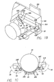
- the invention provides an apparatus for automatically and simultaneously loading a "long" wafer boat or a plurality of wafer boats onto a cantilever paddle, and automatically and/or simultaneously unloading the loaded wafer boats from the cantilever paddle.
- a stationary first track (16-1,43) is aligned with a first opening of a furnace, and a first carriage (42-1) is moveable on the first track, the first carriage (42-1) supporting the first cantilever paddle (47-1).
- the apparatus includes a first vertical translation mechanism (34A), a second vertical translation mechanism (34B), a first horizontal translation mechanism (50A) supported by the first vertical translation mechanism (34A). and a second horizontal translation mechanism (50B) supported by the first vertical translation mechanism.
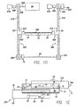
- a second rack gear 78 is attached to the upper surface of base 86.
- a pinion gear 79 is rotatably supported on horizontally moveable intermediate arm 72, causing it to rotate as intermediate horizontally moveable arm 72 moves in the direction of one of arrows 79 as a result of operation of motor 84.
- a pulley 76 is mounted axially with and attached to pinion gear 77.
- Pulley 76 carries a belt 74 which is also supported by an idler pulley 75 at the opposite end of horizontally moveable intermediate arm 72.
- a coupler 73 connects a point on belt 74, which moves in one of the directions of arrows 80, to horizontally moveable arm 51A, causing it to move in one of the directions of arrows 22 in response to operation of motor 84.
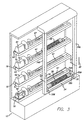
- microcontroller 29 operates to move horizontally moveable arms 51A and 51B and the loaded wafer boats supported thereby over the destination cantilever paddle, for example cantilever paddle 47-1, as shown in Fig. 2A.
- Microcontroller 29 also adjusts for any needed offset correction as previously described to ensure that the wafer boats are precisely aligned with the longitudinal axis of cantilever paddle 47-1.
- Control software of the system 29 causes horizontal translation mechanisms 50A and 50B to perfectly align the up to eight boatloads of wafers over the cantilever paddle 47, and then gently lower them onto cantilever paddle 47 without any abrasion. This is important because it prevents generation of microscopic particulates which, if present, cause imperfections on the integrated circuits being formed and thereby reduce processing yields.
- Microcontroller 29 then operates motor assembly 64 of Fig. 1D to gently rest the wafer boats 26 onto cantilever paddle 47-1.
- the wafer boat loading/unloading mechanism then is operated in the reverse order from that described above to remove each group of loaded wafer boats from the cantilever paddle 47 and return each group to the location shown in Fig. 1A. All of the wafer boats of each group then can be carried away by an operator, or, if available, an automated shuttle machine.
- the upper surface 87A of load platform 87 can be precisely raised and lowered by means of an elongated, inflatable bladder and inflation pump as shown in Fig. 5 to allow wafer boat nest 99 to be lowered enough to clear the lowest portions of boat support assembly 102 and wafer boats 24 as wafer boats 24 are carried between load platform 87 and the location shown in Fig-4C.
Landscapes
- Container, Conveyance, Adherence, Positioning, Of Wafer (AREA)
Applications Claiming Priority (2)
| Application Number | Priority Date | Filing Date | Title |
|---|---|---|---|
| US19251600P | 2000-03-28 | 2000-03-28 | |
| US192516 | 2002-07-08 |
Publications (3)
| Publication Number | Publication Date |
|---|---|
| EP1139392A2 true EP1139392A2 (de) | 2001-10-04 |
| EP1139392A3 EP1139392A3 (de) | 2006-01-25 |
| EP1139392B1 EP1139392B1 (de) | 2007-08-15 |
Family
ID=22709990
Family Applications (1)
| Application Number | Title | Priority Date | Filing Date |
|---|---|---|---|
| EP01107075A Expired - Lifetime EP1139392B1 (de) | 2000-03-28 | 2001-03-21 | Verbesserter Träger für Waferbehälter und Verfahren zum Beladen von zwei Waferbehältern |
Country Status (2)
| Country | Link |
|---|---|
| EP (1) | EP1139392B1 (de) |
| DE (1) | DE60129870D1 (de) |
Cited By (3)
| Publication number | Priority date | Publication date | Assignee | Title |
|---|---|---|---|---|
| CN111525001A (zh) * | 2020-06-01 | 2020-08-11 | 青岛赛瑞达电子装备股份有限公司 | 一种长桨端部支撑装置 |
| CN112117349A (zh) * | 2020-09-09 | 2020-12-22 | 湖州奥博石英科技有限公司 | 一种太阳能电池硅片扩散插片工艺 |
| CN113917172A (zh) * | 2021-11-03 | 2022-01-11 | 北京吉天仪器有限公司 | 自动进样系统和方法 |
Family Cites Families (4)
| Publication number | Priority date | Publication date | Assignee | Title |
|---|---|---|---|---|
| GB8410251D0 (en) * | 1984-04-19 | 1984-05-31 | Heraeus Schott Quarzschmelze | Handling semiconductor wafers |
| JPS62128523A (ja) * | 1985-11-29 | 1987-06-10 | Mitsubishi Electric Corp | ウエ−ハ収納ボ−トの熱処理炉への搬入出装置 |
| KR0129406B1 (ko) * | 1988-03-24 | 1998-04-07 | 카자마 젠쥬 | 반도체 웨이퍼처리장치 |
| US5765982A (en) * | 1995-07-10 | 1998-06-16 | Amtech Systems, Inc. | Automatic wafer boat loading system and method |
-
2001
- 2001-03-21 DE DE60129870T patent/DE60129870D1/de not_active Expired - Lifetime
- 2001-03-21 EP EP01107075A patent/EP1139392B1/de not_active Expired - Lifetime
Cited By (3)
| Publication number | Priority date | Publication date | Assignee | Title |
|---|---|---|---|---|
| CN111525001A (zh) * | 2020-06-01 | 2020-08-11 | 青岛赛瑞达电子装备股份有限公司 | 一种长桨端部支撑装置 |
| CN112117349A (zh) * | 2020-09-09 | 2020-12-22 | 湖州奥博石英科技有限公司 | 一种太阳能电池硅片扩散插片工艺 |
| CN113917172A (zh) * | 2021-11-03 | 2022-01-11 | 北京吉天仪器有限公司 | 自动进样系统和方法 |
Also Published As
| Publication number | Publication date |
|---|---|
| EP1139392B1 (de) | 2007-08-15 |
| DE60129870D1 (de) | 2007-09-27 |
| EP1139392A3 (de) | 2006-01-25 |
Similar Documents
| Publication | Publication Date | Title |
|---|---|---|
| US6537010B2 (en) | Wafer boat support and method for twin tower wafer boat loader | |
| JP6850725B2 (ja) | 基板搬送ロボットおよび基板処理システム | |
| US6279724B1 (en) | Automated semiconductor processing system | |
| US6273110B1 (en) | Automated semiconductor processing system | |
| JPH02297925A (ja) | 縦型cvd拡散装置に於けるウェーハ移載方法及び装置 | |
| US6052913A (en) | Positioning device and positioning method | |
| KR102091915B1 (ko) | 기판 반송 로봇 및 기판 처리 시스템 | |
| WO2000028581A2 (en) | Processing chamber with rapid wafer exchange | |
| WO1995030238A1 (en) | Semiconductor wafer processing system | |
| KR19990021969A (ko) | 기판반송장치 및 그것을 이용한 열처리 시스템 | |
| JP2004524673A (ja) | 自動処理システム | |
| JPH01502866A (ja) | 自動ウェファーローディング方法及び装置 | |
| JPH028120A (ja) | 少なくとも一つの支持体から少なくとも一つの他の支持体へ品物を搬送するための装置 | |
| JP3008758B2 (ja) | タイヤ移載装置 | |
| JPH0230194B2 (de) | ||
| US6352399B1 (en) | Twin tower wafer boat loading system and method | |
| US4664575A (en) | Workpiece transferring apparatus for a robot | |
| JP4690414B2 (ja) | ワーク搬入出システム及び搬送装置 | |
| EP1139392B1 (de) | Verbesserter Träger für Waferbehälter und Verfahren zum Beladen von zwei Waferbehältern | |
| JP2000512218A (ja) | 全方向に傾斜可能なz軸駆動アーム | |
| JPH07106402A (ja) | 板状体搬送装置 | |
| JPH06211320A (ja) | ウエハ搬出搬入装置 | |
| JP3762974B2 (ja) | 搬送装置、並びに、倉庫装置 | |
| JP2002134587A (ja) | 被処理体の搬送機構及び処理システム | |
| KR20010074681A (ko) | 자동 반도체 가공 시스템 |
Legal Events
| Date | Code | Title | Description |
|---|---|---|---|
| PUAI | Public reference made under article 153(3) epc to a published international application that has entered the european phase |
Free format text: ORIGINAL CODE: 0009012 |
|
| 17P | Request for examination filed |
Effective date: 20010321 |
|
| AK | Designated contracting states |
Kind code of ref document: A2 Designated state(s): AT BE CH CY DE DK ES FI FR GB GR IE IT LI LU MC NL PT SE TR |
|
| AX | Request for extension of the european patent |
Free format text: AL;LT;LV;MK;RO;SI |
|
| PUAL | Search report despatched |
Free format text: ORIGINAL CODE: 0009013 |
|
| AK | Designated contracting states |
Kind code of ref document: A3 Designated state(s): AT BE CH CY DE DK ES FI FR GB GR IE IT LI LU MC NL PT SE TR |
|
| AX | Request for extension of the european patent |
Extension state: AL LT LV MK RO SI |
|
| RIC1 | Information provided on ipc code assigned before grant |
Ipc: H01L 21/68 20060101AFI20051202BHEP |
|
| AKX | Designation fees paid |
Designated state(s): DE FR GB IT NL |
|
| GRAP | Despatch of communication of intention to grant a patent |
Free format text: ORIGINAL CODE: EPIDOSNIGR1 |
|
| GRAS | Grant fee paid |
Free format text: ORIGINAL CODE: EPIDOSNIGR3 |
|
| GRAA | (expected) grant |
Free format text: ORIGINAL CODE: 0009210 |
|
| AK | Designated contracting states |
Kind code of ref document: B1 Designated state(s): DE FR GB IT NL |
|
| REG | Reference to a national code |
Ref country code: GB Ref legal event code: FG4D |
|
| REF | Corresponds to: |
Ref document number: 60129870 Country of ref document: DE Date of ref document: 20070927 Kind code of ref document: P |
|
| ET | Fr: translation filed | ||
| PG25 | Lapsed in a contracting state [announced via postgrant information from national office to epo] |
Ref country code: NL Free format text: LAPSE BECAUSE OF FAILURE TO SUBMIT A TRANSLATION OF THE DESCRIPTION OR TO PAY THE FEE WITHIN THE PRESCRIBED TIME-LIMIT Effective date: 20070815 |
|
| NLV1 | Nl: lapsed or annulled due to failure to fulfill the requirements of art. 29p and 29m of the patents act | ||
| PLBE | No opposition filed within time limit |
Free format text: ORIGINAL CODE: 0009261 |
|
| STAA | Information on the status of an ep patent application or granted ep patent |
Free format text: STATUS: NO OPPOSITION FILED WITHIN TIME LIMIT |
|
| 26N | No opposition filed |
Effective date: 20080516 |
|
| PG25 | Lapsed in a contracting state [announced via postgrant information from national office to epo] |
Ref country code: DE Free format text: LAPSE BECAUSE OF FAILURE TO SUBMIT A TRANSLATION OF THE DESCRIPTION OR TO PAY THE FEE WITHIN THE PRESCRIBED TIME-LIMIT Effective date: 20071116 |
|
| PGFP | Annual fee paid to national office [announced via postgrant information from national office to epo] |
Ref country code: GB Payment date: 20080530 Year of fee payment: 8 |
|
| GBPC | Gb: european patent ceased through non-payment of renewal fee |
Effective date: 20090321 |
|
| PG25 | Lapsed in a contracting state [announced via postgrant information from national office to epo] |
Ref country code: GB Free format text: LAPSE BECAUSE OF NON-PAYMENT OF DUE FEES Effective date: 20090321 |
|
| PG25 | Lapsed in a contracting state [announced via postgrant information from national office to epo] |
Ref country code: IT Free format text: LAPSE BECAUSE OF NON-PAYMENT OF DUE FEES Effective date: 20080331 |
|
| REG | Reference to a national code |
Ref country code: FR Ref legal event code: PLFP Year of fee payment: 16 |
|
| PGFP | Annual fee paid to national office [announced via postgrant information from national office to epo] |
Ref country code: FR Payment date: 20160328 Year of fee payment: 16 |
|
| REG | Reference to a national code |
Ref country code: FR Ref legal event code: ST Effective date: 20171130 |
|
| PG25 | Lapsed in a contracting state [announced via postgrant information from national office to epo] |
Ref country code: FR Free format text: LAPSE BECAUSE OF NON-PAYMENT OF DUE FEES Effective date: 20170331 |