EP1139486A1 - Dispositif non-réciproque et dispositif de communication l'incorporant - Google Patents
Dispositif non-réciproque et dispositif de communication l'incorporant Download PDFInfo
- Publication number
- EP1139486A1 EP1139486A1 EP01107516A EP01107516A EP1139486A1 EP 1139486 A1 EP1139486 A1 EP 1139486A1 EP 01107516 A EP01107516 A EP 01107516A EP 01107516 A EP01107516 A EP 01107516A EP 1139486 A1 EP1139486 A1 EP 1139486A1
- Authority
- EP
- European Patent Office
- Prior art keywords
- conductor
- circuit device
- reciprocal circuit
- composite base
- laminate
- Prior art date
- Legal status (The legal status is an assumption and is not a legal conclusion. Google has not performed a legal analysis and makes no representation as to the accuracy of the status listed.)
- Withdrawn
Links
- 239000004020 conductor Substances 0.000 claims abstract description 208
- 239000002131 composite material Substances 0.000 claims abstract description 90
- 239000003990 capacitor Substances 0.000 claims abstract description 61
- 239000002184 metal Substances 0.000 claims abstract description 24
- 229910052751 metal Inorganic materials 0.000 claims abstract description 24
- 238000009413 insulation Methods 0.000 claims abstract description 11
- 239000000919 ceramic Substances 0.000 claims description 25
- 230000005540 biological transmission Effects 0.000 claims description 12
- 229920005992 thermoplastic resin Polymers 0.000 claims description 11
- 230000001413 cellular effect Effects 0.000 claims description 9
- 230000004907 flux Effects 0.000 claims description 4
- 239000002223 garnet Substances 0.000 description 13
- 238000005245 sintering Methods 0.000 description 13
- RYGMFSIKBFXOCR-UHFFFAOYSA-N Copper Chemical compound [Cu] RYGMFSIKBFXOCR-UHFFFAOYSA-N 0.000 description 12
- 229910052802 copper Inorganic materials 0.000 description 12
- 239000010949 copper Substances 0.000 description 12
- 238000004519 manufacturing process Methods 0.000 description 12
- XEEYBQQBJWHFJM-UHFFFAOYSA-N Iron Chemical compound [Fe] XEEYBQQBJWHFJM-UHFFFAOYSA-N 0.000 description 8
- BQCADISMDOOEFD-UHFFFAOYSA-N Silver Chemical compound [Ag] BQCADISMDOOEFD-UHFFFAOYSA-N 0.000 description 8
- 229910052709 silver Inorganic materials 0.000 description 8
- 239000004332 silver Substances 0.000 description 8
- 238000010030 laminating Methods 0.000 description 6
- 229910000679 solder Inorganic materials 0.000 description 5
- 238000005476 soldering Methods 0.000 description 5
- 229910052742 iron Inorganic materials 0.000 description 4
- 150000002739 metals Chemical class 0.000 description 4
- 238000007747 plating Methods 0.000 description 4
- -1 polyethylene Polymers 0.000 description 4
- 229910045601 alloy Inorganic materials 0.000 description 3
- 239000000956 alloy Substances 0.000 description 3
- 239000007772 electrode material Substances 0.000 description 3
- 230000003628 erosive effect Effects 0.000 description 3
- PCHJSUWPFVWCPO-UHFFFAOYSA-N gold Chemical compound [Au] PCHJSUWPFVWCPO-UHFFFAOYSA-N 0.000 description 3
- 238000003780 insertion Methods 0.000 description 3
- 230000037431 insertion Effects 0.000 description 3
- 238000000034 method Methods 0.000 description 3
- 238000003825 pressing Methods 0.000 description 3
- VYPSYNLAJGMNEJ-UHFFFAOYSA-N Silicium dioxide Chemical compound O=[Si]=O VYPSYNLAJGMNEJ-UHFFFAOYSA-N 0.000 description 2
- 125000003118 aryl group Chemical group 0.000 description 2
- 238000005336 cracking Methods 0.000 description 2
- 238000010586 diagram Methods 0.000 description 2
- 229910052737 gold Inorganic materials 0.000 description 2
- 239000010931 gold Substances 0.000 description 2
- 239000004973 liquid crystal related substance Substances 0.000 description 2
- 238000005259 measurement Methods 0.000 description 2
- 238000000465 moulding Methods 0.000 description 2
- 229920000139 polyethylene terephthalate Polymers 0.000 description 2
- 239000005020 polyethylene terephthalate Substances 0.000 description 2
- 229920000642 polymer Polymers 0.000 description 2
- 238000012360 testing method Methods 0.000 description 2
- 229910001369 Brass Inorganic materials 0.000 description 1
- 229910000906 Bronze Inorganic materials 0.000 description 1
- 229910017061 Fe Co Inorganic materials 0.000 description 1
- 229910003271 Ni-Fe Inorganic materials 0.000 description 1
- OAICVXFJPJFONN-UHFFFAOYSA-N Phosphorus Chemical compound [P] OAICVXFJPJFONN-UHFFFAOYSA-N 0.000 description 1
- 239000004698 Polyethylene Substances 0.000 description 1
- 239000004734 Polyphenylene sulfide Substances 0.000 description 1
- 239000004743 Polypropylene Substances 0.000 description 1
- 229910000831 Steel Inorganic materials 0.000 description 1
- 230000015572 biosynthetic process Effects 0.000 description 1
- 239000010951 brass Substances 0.000 description 1
- 239000010974 bronze Substances 0.000 description 1
- 239000010960 cold rolled steel Substances 0.000 description 1
- 239000000470 constituent Substances 0.000 description 1
- KUNSUQLRTQLHQQ-UHFFFAOYSA-N copper tin Chemical compound [Cu].[Sn] KUNSUQLRTQLHQQ-UHFFFAOYSA-N 0.000 description 1
- 230000003247 decreasing effect Effects 0.000 description 1
- 230000007547 defect Effects 0.000 description 1
- 230000006866 deterioration Effects 0.000 description 1
- 239000003989 dielectric material Substances 0.000 description 1
- 230000000694 effects Effects 0.000 description 1
- 238000005530 etching Methods 0.000 description 1
- 239000000945 filler Substances 0.000 description 1
- 230000012447 hatching Effects 0.000 description 1
- 238000001746 injection moulding Methods 0.000 description 1
- 239000011810 insulating material Substances 0.000 description 1
- 229910000765 intermetallic Inorganic materials 0.000 description 1
- LQBJWKCYZGMFEV-UHFFFAOYSA-N lead tin Chemical compound [Sn].[Pb] LQBJWKCYZGMFEV-UHFFFAOYSA-N 0.000 description 1
- 239000000463 material Substances 0.000 description 1
- 239000007769 metal material Substances 0.000 description 1
- 238000012986 modification Methods 0.000 description 1
- 230000004048 modification Effects 0.000 description 1
- 238000005192 partition Methods 0.000 description 1
- 229920000573 polyethylene Polymers 0.000 description 1
- 229920000069 polyphenylene sulfide Polymers 0.000 description 1
- 229920001155 polypropylene Polymers 0.000 description 1
- 239000000843 powder Substances 0.000 description 1
- 229920005989 resin Polymers 0.000 description 1
- 239000011347 resin Substances 0.000 description 1
- 238000004904 shortening Methods 0.000 description 1
- 239000000377 silicon dioxide Substances 0.000 description 1
- 239000010959 steel Substances 0.000 description 1
- 229920003002 synthetic resin Polymers 0.000 description 1
- 239000000057 synthetic resin Substances 0.000 description 1
- 229920001169 thermoplastic Polymers 0.000 description 1
- 239000004416 thermosoftening plastic Substances 0.000 description 1
- 229910000859 α-Fe Inorganic materials 0.000 description 1
Images


Classifications
-
- H—ELECTRICITY
- H01—ELECTRIC ELEMENTS
- H01P—WAVEGUIDES; RESONATORS, LINES, OR OTHER DEVICES OF THE WAVEGUIDE TYPE
- H01P1/00—Auxiliary devices
- H01P1/32—Non-reciprocal transmission devices
-
- H—ELECTRICITY
- H01—ELECTRIC ELEMENTS
- H01P—WAVEGUIDES; RESONATORS, LINES, OR OTHER DEVICES OF THE WAVEGUIDE TYPE
- H01P1/00—Auxiliary devices
- H01P1/32—Non-reciprocal transmission devices
- H01P1/38—Circulators
- H01P1/383—Junction circulators, e.g. Y-circulators
- H01P1/387—Strip line circulators
Definitions
- the present invention relates to a non-reciprocal circuit device such as a circulator, an isolator, etc., particularly to a miniaturized, low-loss, highly reliable non-reciprocal circuit device and wireless communications equipment such as a cellular phone comprising such a non-reciprocal circuit device.
- Non-reciprocal circuit devices such as circulators, isolators, etc. have characteristics of transmitting a signal to only a particular direction while preventing the signal from being transmitted in the opposite direction, and thus are indispensable parts for transmission circuits of microwave transmission equipment for automobile phones, etc. In such applications, the non-reciprocal circuit devices are required to be miniaturized and reduced in loss.
- a non-reciprocal circuit device for instance, an isolator, comprises a magnetic body such as a garnet member, etc., three central conductors disposed on the magnetic body such as a garnet member while overlapping at a 120° interval with electric insulation from each other, a permanent magnet for applying a DC magnetic field to the magnetic body, matching capacitors and a metal case serving as a magnetic yoke and containing these parts.
- Fig. 15 shows an isolator, one example of the conventional non-reciprocal circuit devices, disclosed in Japanese Patent Laid-Open No. 11-205011.
- This isolator comprises a box-shaped resin-conductor composite base 96 disposed on a lower case 92, the resin-conductor composite base 96 having recesses 100 for respectively receiving a central conductor assembly 4 comprising three central conductors 11a-11c disposed on a garnet member 12 with electric insulation from each other, matching capacitors constituted by three flat capacitors 94a-94c, and a chip resistor 95.
- Each recess 100 of the resin-conductor composite base 96 is defined by an insulating thermoplastic resin partition 101 for positioning each part.
- a ground electrode 102 (indicated by hatching) for connecting the central conductor assembly 4 and the capacitors 94a-94c to a ground.
- Each central conductor 11a-11c has one end connected to an electrode of each capacitor 94a-94c and the other end connected to a ground electrode 102 on the resin-conductor composite base 96.
- Each flat capacitor 94a-94c has two opposing electrodes, one connected to each central conductor 11a-11c, and the other connected to the ground conductor 102.
- a resistor 95 is connected to the flat capacitor 94c in parallel.
- a permanent magnet 93 for applying a DC magnetic field to the central conductor assembly 4 is disposed in an upper case 91, which is combined with the lower case 92 to constitute an isolator.
- Each of the upper case 91 and the lower case 92 is formed by an iron-based magnetic sheet such as SPCC (cold-rolled steel sheet) plated with silver for functioning as a magnetic yoke constituting a magnetic circuit for applying a magnetic force of the permanent magnet 93 to the central conductor assembly 4.
- a conductor plate constituting the ground electrode 102 in the resin-conductor composite base 96 is bent to integrally have ground terminals 97b, 97c exposing from the lower and side surfaces of the resin-conductor composite base, exposed portions of the conductor plate being plated with silver.
- the resin-conductor composite base 96 is provided on a lower surface with an input/output terminal 97a and ground terminals 97b, 97c.
- each of the two central conductors 11a, 11b has one end connected to the input/output terminal 97a via the flat capacitor 94a, 94b, and the other end connected to the ground terminal 97b, 97c via the ground electrode 102.
- the remaining one central conductor 11c is connected to the ground terminal 102 for termination via the capacitor 94c and the resistor 95.
- Fig. 16 shows an isolator, another example of the conventional non-reciprocal circuit devices, disclosed in Japanese Patent Laid-Open No. 9-55607.
- This isolator has matching capacitors formed inside a laminate module 105 disposed on a lower case 92, and the laminate module 105 having a center opening 110 for receiving a garnet member 12 and a central conductor assembly 4 constituted by three central conductors 11a-11c, one end of each of three central conductors 11a-11c being connected to a capacitor 106a-106c printed on an upper surface of the laminate module 105.
- a capacitor 106c connected to one central conductor 11c is electrically connected to a resistor 107 in parallel.
- a permanent magnet 93 for applying a DC magnetic field to the central conductor assembly 4 is disposed in the upper case 91, which is assembled to the lower case 92 to constitute an isolator.
- the laminate module 105 has projections 112 on both sides of a lower surface thereof, onto which an input/output terminal and ground terminals (not shown) are mounted, and a recess 114 between the two projections 112 is formed with an electrode (not shown) for connecting to the lower case, whereby the ground terminals are connected to the lower case-connecting electrodes.
- the other ends of the central conductors 11a-11c namely the side of the central conductors 11a-11c connected to the lower case 92, are connected to a ground in a circuit board via the lower case 92 and the lower case-connecting electrode and the ground terminals 108b, 108c of the laminate module 105.
- C ⁇ r ⁇ o ⁇ S/d
- C is a capacitance of a capacitor
- ⁇ r is a specific dielectric constant of a dielectric body
- ⁇ o is a dielectric constant of vacuum
- S is an area of an electrode
- d is a thickness of a dielectric body between the electrodes.
- the formula (1) indicates that to keep the same level of capacitance even when the electrode area S is reduced by the miniaturization of the matching capacitor, it is necessary to use a dielectric body with a large specific dielectric constant ⁇ r or to reduce the thickness d of a dielectric body between the electrodes.
- dielectric bodies having large specific dielectric constants generally tend to have large dielectric loss, resulting in the loss characteristics of capacitors and thus increase in the loss of isolators.
- a dielectric body disposed between the electrodes has a small thickness
- its handling is difficult during the production process, resulting in cracking and breakage of capacitors, leading to a poor yield.
- a garnet member has a small diameter
- a central conductor assembly comprising the central conductors and the garnet member has a small inductance, necessitating the capacitors to have larger capacitance to operate at the same operation frequency, causing the same problems as the miniaturization of the capacitors.
- the garnet member having a larger thickness can increase the inductance of the central conductor assembly, it undesirably hinders the reduction of the thickness of an isolator.
- the miniaturization of parts such as the capacitors and the garnet member results in the complicated structure of a box-shaped resin-conductor composite base, making it difficult to produce the resin-conductor composite base.
- the isolator of Japanese Patent Laid-Open No. 9-55607 has a structure in which matching capacitors are formed inside the laminate module 105, it is considered that capacitance can easily be obtained by forming capacitors in a plurality of layers of the laminate module.
- the miniaturization of the laminate module is expected, because the above structure makes it easy to reduce an electrode area of a capacitor without reducing capacitance.
- the above isolator uses a laminate module 105 having an opening 110
- the other ends of the central conductors 11a-11c are directly soldered to the lower case 92
- lower case-connecting electrodes (not shown) in the recess 114 on the lower surface of the laminate module 105 are soldered to the lower case 92.
- the lower case-connecting electrodes on the lower surface of the laminate module 105 are connected to ground terminals 108b, 108c, the other ends of the central conductors 11a-11c are grounded via the lower case 92 and lower case-connecting electrodes on the lower surface of the laminate module 105.
- the case is made of highly conductive materials such as silver, copper, etc., or it is provided with as thick plating or electrode as 30 ⁇ m or more to reduce electric resistance.
- the lower case 92 is made of an iron-based metal, because it constitutes a magnetic yoke, thereby having a relatively low electric conductivity.
- the case is as expensive as two times or more than otherwise.
- the electrode cannot be made fully thick, resulting in poor electric conductivity in the lower case-connecting electrodes directly formed on the laminate module 105, making it difficult to ground the central conductors without loss. Thus, large loss cannot be avoided in the above isolator.
- external terminals 108a-108c are integrally formed on the bottom or side surfaces of the laminate module 105 for connection to a circuit board. It is considered that the laminate module 105 provided with external terminals is superior to a resin-conductor composite base provided with external terminals like the isolator as shown in Fig. 15, because of a smaller number of parts.
- stress would be concentrated on the external terminals of the isolator, if the parts-mounting circuit board forming the external circuit is deformed for some reasons, for instance, by dropping a mobile terminal, etc. Therefore, the laminate module 105 is easily broken, resulting in breakage of the isolator.
- ridges 112 should be provided on both side ends on the lower surface of the laminate module 105 to provide the laminate module 105 with external terminals 108a-108c.
- such integral steps make it impossible to press green sheets uniformly in a plane, leaving difference in density between the ridges and the recesses.
- This difference in press density leads to difference in a sintering shrinkage ratio between the ridges and the recesses, resulting in a deformed laminate module 105 after sintering.
- the external terminals have poor flatness, resulting in poor connection to the external circuit on the circuit board.
- a vertical load may be applied to the laminate module during sintering to suppress its deformation in a plane, this makes the sintering process complicated, undesirably increasing production cost.
- an object of the present invention is to provide a miniaturized, low-loss, high-reliability, easy-to-produce non-reciprocal circuit device, and a wireless communications equipment comprising such a non-reciprocal circuit device.
- the non-reciprocal circuit device of the present invention comprises a plurality of central conductors overlapping with electric insulation from each other at a predetermined angle, a magnetic body disposed in contact with or close to the central conductors, matching capacitors, a permanent magnet disposed for applying a DC magnetic field to the central conductors and the magnetic body, and metal cases for receiving these parts and serving as a magnetic yoke, at least the matching capacitors being integrally constituted in a laminate module having a substantially flat lower surface, and the laminate module being disposed on a substantially flat surface of a composite base comprising an insulation member and conductor plates.
- the matching capacitors are formed in the laminate module in single or plural layers, the number of layers may be properly set to obtain the desired capacitance. Therefore, the capacitance of capacitors can be increased without increasing an electrode area. Because a reduced electrode area can be achieved with the same capacitance, the laminate module constituting capacitors can be miniaturized, resulting in miniaturization of an isolator. Further, by selecting materials having a small dielectric constant for the laminate module, the capacitors can be provided with reduced dielectric loss, thereby improving the loss characteristics of the isolator.
- the laminate module having a flat lower surface is directly disposed on a flat upper surface of the composite base, a wide contact area can be obtained between both ground electrodes. Also, the composite base is disposed on the lower case, and the laminate module is disposed thereon, resulting in easiness in assembling of parts.
- the composite base comprises a ground electrode connected to the central conductors and the capacitors of the laminate module and terminal electrodes connected to the central conductors and the capacitors of the laminate module on the same plane, the ground terminals connected to the ground electrode and the input/output terminals connected to the terminal electrodes being provided as external terminals on side surfaces and/or a lower surface of the laminate module.
- the laminate module has a ground electrode for connecting the capacitors to a ground on a substantially entire lower surface thereof, the ground electrode of the laminate module being disposed directly on a substantially entire upper surface of a ground electrode of the composite base and electrically connected thereto, and the ground electrode of the composite base being disposed directly on a lower metal case and electrically connected thereto.
- the lower surface of the laminate module is in close contact with the ground electrode (conductor plate) of the composite base and directly soldered to each other.
- the ground electrode (conductor plate) on a lower surface of the composite base is in close contact with the upper surface of the lower base and directly soldered to each other. Because this provides a wide contact area, the insertion loss is decreased, thereby providing good connection of the ground electrode and the terminal electrodes without loss. Further, it provides geed characteristics of attenuating second and third harmonic, and improved mechanical strength.
- the close contact of the laminate module and the resin-conductor composite base to the lower case without gap is an important feature of the present invention.
- external terminals such as the ground terminals connected to the ground electrode and the input/output terminals connected to the terminal electrodes, they are integrally formed on side surfaces and/or a lower surface of the composite base with a conductor plate, low loss can be achieved. Also, because the lower surface of the resin-conductor composite base is highly flat, insufficient contact is not likely with a test board or a parts-mounting circuit board, thereby providing a non-reciprocal circuit device with stable characteristics.
- the composite base is desirably a resin-conductor composite base comprising conductor plates having an electric resistance of 5.5 x 10 -8 ⁇ m or less integrally molded with an insulating thermoplastic resin.
- insulating materials forming the laminate module may be synthetic resins and ceramics, insulating thermoplastic resins such as polyethylene, polypropylene, polyethylene terephthalate (PET), etc. are preferable from the aspect of easy of production and impact resistance. Considering strength and heat resistance, it is preferable to use insulating thermoplastic engineering resins such as liquid-crystal, aromatic polymers containing silica fillers, polyphenylene sulfide, etc.
- the conductor plate may be made of steel such as SPCC, copper, silver and other metals having the same low electric resistance preferable. Specifically, high-conductivity metals having electric resistance of 5.5 x 10 -8 ⁇ m or less or metals plated with silver or copper are preferable. From the aspect of erosion of a circuit board with solder, a copper plate is preferable. From the aspect of formability, a metal plate of 0.03-0.15 mm in thickness is preferable.
- the terminal electrodes and at least one input/output terminal are integrally formed by the same conductor plate in the resin-conductor composite base. With this structure, an electric resistance can extremely be reduced between the terminal electrodes and the input/output terminals of the resin-conductor composite base, thereby remarkably suppressing electric loss in the connection of the central conductors and the capacitors to the external circuit.
- a ground electrode and at least one ground terminal are preferably integrally formed by the same conductor plate in the resin-conductor composite base.
- the ground electrode and the terminal electrodes of the resin-conductor composite base preferably have contact surfaces in the same plane.
- the laminate module has input/output electrodes connected to the terminals of the resin-conductor composite base and a ground electrode connected to the ground electrode of the resin-conductor composite base in the same plane on a surface in contact with the resin-conductor composite base.
- the resin-conductor composite base preferably has a means for positioning the laminate module on a flat upper surface thereof.
- a positioning means is, for instance, external terminals provided on side surfaces of the resin-conductor composite base.
- the central conductors are preferably formed in an integral central conductor laminate comprising a plurality of ceramic sheets having central conductor patterns.
- the ceramic sheets are preferably formed of magnetic ceramics such as garnet.
- This structure makes it possible to form the capacitors and the central conductors into an integral laminate, thereby achieving the miniaturization of the non-reciprocal circuit device, the simplification of its structure, and thus shortening the production processes. Also, to obtain high dimension accuracy and stable electric characteristics, it is effective to use a central conductor assembly comprising central conductors formed from a copper plate by etching, which are wound around a microwave magnetic, sintered ferrite member at a predetermined angle.
- the electrode patterns in the laminate module are preferably connected through via-electrodes and/or side-surface electrodes.
- the electrode patterns in the central conductor laminate are preferably connected through via-electrodes and/or side-surface electrodes.
- via-electrodes the number of production can be reduced to lower the production cost of the non-reciprocal circuit device, though they are slightly disadvantageous in miniaturization.
- the non-reciprocal circuit device can be further miniaturized. Using both via-electrodes and electrodes printed on side surfaces, the resistance of conductors can be suppressed while compensating defects of both electrodes, thereby achieving low loss.
- the central conductors are preferably bent along an outer surface of the magnetic body, and insulation films are disposed between the central conductors in their crossing portions.
- the central conductors and the magnetic body are formed by an integral laminate comprising a plurality of ceramic sheets having central conductor patterns.
- At least a lower case of the metal cases is formed by an integral laminate of a metal having as high saturation magnetic flux density as 0.6 T or more clad with a high-conductivity metal having an electric resistance of 5.5 x 10 -8 ⁇ m or less, whereby the lower case serves as an electrically conductive magnetic yoke.
- the wireless communications equipment of the present invention comprises the above non-reciprocal circuit device, a transmission circuit, a reception circuit, and an antenna.
- the wireless communications equipment is preferably a cellular phone.
- the present invention is characterized in that a miniaturized, low-loss, high-reliability non-reciprocal circuit device is obtained by constituting at least matching capacitors in a laminate module, electrically conducting an internal circuit of the laminate module to an external circuit of a parts-mounting circuit board via external terminals mounted onto a composite base (resin-conductor composite base), and by connecting the laminate module to the resin-conductor composite base and the lower case by placing them in a plane.
- the laminate module is obtained by printing electrodes on ceramic green sheets, laminating and pressing the green sheets, and then sintering them, like laminate chips.
- the internal electrodes of the laminate module are formed at the same time as sintering the ceramic. Electrodes on the side surfaces of the laminate module may be formed by sintering together with the ceramic, or by printing an electrode material on the sintered ceramic green sheets, and laminating and burning them.
- the non-reciprocal circuit device is exemplified by an isolator, though it is not restricted to an isolator, because a circulator can be constituted when one capacitor is not terminated by a resistor.
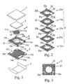
- Fig. 1 is an exploded perspective view showing an isolator according to the first embodiment of the present invention.
- This isolator comprises a laminate module 5 and a central conductor assembly 4 disposed on a resin-conductor composite base 6, a permanent magnet 3 disposed thereon for applying a DC magnetic field to the central conductor assembly 4, and metal cases 1, 2 serving as a magnetic yoke and enclosing these parts vertically.
- the central conductor assembly 4 may basically have the same structure as that of the above-described conventional one.
- a disc-shaped magnetic body made of garnet, etc.
- the central conductor assembly 4 is inserted into a center bore 10 of the laminate module 5, with one end of each central conductor 11a-11c connected to an electrode 13a-13c of each capacitor on an upper surface of the laminate module 5, and with the other end of each central conductor 11a-11c connected to a ground electrode (conductor plate) 18 of the resin-conductor composite base 6 via a ground conductor positioning on a lower surface of the garnet member 12.
- the laminate module 5 is constituted by laminating dielectric ceramic green sheets 21a-21e printed with electrode patterns 22a-22c, 23a-23c and 24a-24c for forming capacitors and a ground electrode 24, the electrode patterns 22a, 23a, 24a forming an input-side capacitor, the electrode patterns 22b, 23b, 24b forming an output-side capacitor, and the electrode patterns 22c, 23c, 24c forming a load-side capacitor.
- These green sheets 21a-21e are laminated, pressed and then sintered to form each capacitor. Electrodes inside the laminate module 5 are formed at the same time as sintering a ceramic. In this laminate module 5, the load electrodes 22c, 23c, 24c are connected through a via-electrode 26.
- connection of electrodes existing on different layers are achieved with side-surface electrodes formed by printing an electrode material on side surfaces of the laminate module 5 after sintering and burning it, like a side-surface electrode 14a for connecting the electrodes 22a, 23a, 24a.
- the electrodes 22a, 23a, 24a and 22b, 23b, 24b for capacitors may be connected through via-electrodes.
- the ground electrodes 14b, 14c are also formed as side-surface electrodes.
- the bore 10 may be provided substantially at a center of the laminate module 5 by laminating green sheets 21a-21e each having a bore 25, though the bore 10 is preferably provided in a laminate block obtained by laminating and pressing the green sheets.
- a resistor 15 is formed on the upper surface of the laminate module 5 by printing and burning.
- a chip resistor may be used in place of the printed resistor, and a resistor may be formed by simultaneous burning with the ceramic.
- input/output electrodes 28a, 28b connectable to terminal electrodes 16a, 16b (separate conductor plates) of the resin-conductor composite base 6 are formed at corners on a lower surface of the laminate module 5, namely a surface of the laminate module 5, which is to be in contact with the ground electrode 18 (conductor plate) of the resin-conductor composite base 6.
- a ground electrode 27, which is to be in contact with the ground electrode 18 of the resin-conductor composite base 6, is formed on an entire lower surface of the laminate module 5 except for exposed portions surrounding the input/output electrodes 28a, 28b.
- This ground electrode 27 is adapted to be brought into contact with substantially the entire flat, upper surface of the ground electrode 18 (conductor plate) of the resin-conductor composite base 6, and a substantially entire lower surface of the ground electrode 18 is adapted to be in contact with a lower metal case 2. Thereafter, a contact portion is electrically connected by solder reflow.
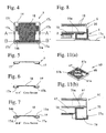
- Figs. 4 and 5 are respectively a plan view and a side view of the resin-conductor composite base 6, Fig. 6 is a cross-sectional view taken along the line A-A' in Fig. 4, and Fig. 7 is a cross-sectional view taken along the line B-B' in Fig. 4.
- hatched portions are conductor plates, and white portions are insulating thermoplastic resin portions.
- an upper surface of the resin-conductor composite base 6, which is brought into contact with the lower surface of the laminate module 5 is in a flat plane including the ground electrode 18 (conductor plate) and an insulating thermoplastic resin portion 19.
- the ground electrode 18 and ground terminals 17b, 17c, 17e, 17f are integrally constituted by a single conductor plate I.
- the ground electrode 18 and the terminal electrodes 16a, 16b are formed on the same flat plane.
- a terminal electrode 16a on the input side and an input external terminal 17a are integrally constituted by another single conductor plate II.
- a terminal electrode 16b on the output side and an output external terminal 17d are integrally constituted by a still further single conductor plate III.
- the conductor plates I, II, III constitute the same flat plane.
- Each conductor plate I, II, III may be a 0.1-mm-thick copper plate, for instance, and integrally molded into the resin-conductor composite base 6 by an insert molding method using a liquid-crystal, aromatic polymer ("Sumika Super,” available from Sumitomo Chemical Co., Ltd.).
- a copper plate is preferable, because it is excellent in workability and insertion loss-decreasing effects, free from problems such as erosion with solder.
- the ground electrode 18 and the ground terminals 17b, 17c, 17e, 17f are constituted by the same conductor plate in the resin-conductor composite base 6, there is extremely small electric resistance between the ground electrode 18 and the ground terminals 17b, 17c, 17e, 17f. Therefore, the ground electrode 27 of the laminate module 5 is grounded with small loss. Also, because the terminal electrode 16a and the input/output terminal 17a are constituted by the same conductor plate, there is extremely small electric resistance between the terminal electrode 16a and the input/output terminal 17a. Further, because the terminal electrode 16b and the input/output terminal 17d are constituted by the same conductor plate, there is extremely small electric resistance between the terminal electrode 16b and the input/output terminal 17d. Accordingly, the input/output electrodes 28a, 28b of the laminate module 5 are connected to the input and output circuits with small loss.
- the external terminals 17a-17f (input/output terminals and ground electrode) formed on the resin-conductor composite base 6 are connected to an external circuit. Because of this structure, even when an external circuit board, onto which the laminate module 5 is mounted, is deformed for some external causes, a stress that would otherwise be applied to the laminate module 5 would be absorbed by conductor plates of the external terminals 17a-17f and an insulating thermoplastic resin portion around the conductor plates in the resin-conductor composite base 6. Accordingly, strong connection is kept between the external circuit and the isolator, which is less likely to be damaged. Further, because the external terminals provided on a lower surface of the resin-conductor composite base 6 are flat, insufficient contact is not likely between the external terminals and the laminate module-mounting circuit board.
- a projection 20 extending from the external terminal 17a can serve as a positioning means for the laminate module 5 on a surface of the resin-conductor composite base 6, which is brought into contact with the laminate module 5, thereby facilitating the assembling.
- a plurality of such structures may be provided in other portions.
- a miniaturized, low-loss isolator having an outer size of 4 mm x 4 mm x 1.7 mm, for instance, can be obtained.
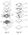
- Fig. 9 shows an isolator according to the second embodiment of the present invention.
- This isolator differs from that of the first embodiment in the structures of the laminated central conductor assembly 40 and the laminate module 50.
- the laminated central conductor assembly (central conductor laminate) 40 of this embodiment is formed by printing central conductor patterns 44a-44c onto magnetic ceramic green sheets 43a-43f, laminating and pressing these green sheets 43a-43f and sintering them.
- the magnetic ceramic green sheets are formed from garnet powder.
- Capacitor-connecting electrodes 41a-41c for connecting ends of central conductors 44a-44c to capacitor electrodes 51a-51c on the laminate module 50, a grounding electrode 45 provided on a lower surface of the central conductor laminate 40, and side-surface electrodes 42 for connecting the other ends of central conductors 44a-44c to the grounding electrode 45 may be formed on the central conductor laminate 40, by printing green sheets and burning the printed electrodes and the ceramic green sheets simultaneously, or by printing electrodes on sintered ceramic sheets and burning the electrodes.
- the grounding conductor 45 of the central conductor laminate 40 is placed on the ground electrode 18 of the resin-conductor composite base 6 and electrically connected by soldering.
- the electrodes 51a-51c of capacitors in the laminate module 50 of this embodiment are connected to input/output electrodes and a ground electrode (not shown) on a lower surface of the laminate module through via-electrodes provided in the laminate module 50.
- the laminate module 50 is provided with a rectangular through-hole 55 corresponding to the central conductor laminate 40 substantially at a center thereof. Further, formed inside the through-hole 55 are internal electrodes 52a, 52b, 52c for connecting the capacitor electrodes 51a-51c to the capacitor-connecting electrodes 41a-41c of the central conductor laminate 40.
- the internal electrodes 52a-52c may be formed by simultaneous burning with ceramic or by printing sintered, laminated ceramic sheets and burning them.
- the capacitor-connecting electrodes 41a-41c may be soldered to the internal electrodes 52a-52c via so-called side through-holes.
- the central conductor laminate 40 and the center through-hole 55 of the laminate module 50 having the same shape, the central conductor laminate 40 can easily be positioned and connected to the laminate module 50. Because the other parts such as a resin-conductor composite base, etc. may be the same as those in the first embodiment, their explanation will be omitted here.
- Fig. 11 shows an isolator according to the third embodiment of the present invention. While the central conductor laminate 40 comprising central conductors inside a magnetic body is combined with the laminate module 50 comprising capacitors therein in the second embodiment, the isolator according to the third embodiment comprises central conductors 67 formed on a surface and inside of a laminate module 60 as shown in Fig. 11(a), with a magnetic body 62 disposed between a resin-conductor composite base 70 and the laminate module 60 as shown in Fig. 11(b).
- an upper surface of the magnetic body 62 disposed on the resin-conductor composite base 70 is in the same plane as the upper surface of the resin-conductor composite base 70. Accordingly, the laminate module 60 having a flat lower surface can be disposed on the ground electrode 78 and the magnetic body 62.
- Fig. 12 shows an isolator according to the fourth embodiment of the present invention. Because an upper case 1, a permanent magnet 3, a central conductor assembly 4, a laminate module 5 and external terminals in the fourth embodiment are the same as those in the first embodiment, the same reference numerals as in Fig. 1 are given to them in Fig. 12. In this embodiment, the same resin-conductor composite base 6 and the same lower case 2 as in the first embodiment are integrally molded together to provide a resin-conductor composite base 7.
- the resin-conductor composite base 7 is obtained by placing a conductor plate 71 punched and bent to have a portion constituting a ground electrode, portions constituting external terminals, and upright portions 70 of a lower case, a conductor plate 72 constituting a terminal electrode 16a and an input external terminal 17a, a conductor plate 73 constituting a terminal electrode 16b and an output external terminal 17d in a molding die such that these conductor plates are positioned on the same plane, and integrally injection-molding them with an insulating thermoplastic resin 19. Because two parts of the resin-conductor composite base and the lower case in the first embodiment are integrated into a single part as the resin-conductor composite base 7, the number of parts used is reduced, resulting in decrease in the number of assembling steps.
- the lower case comprising a conductor plate 71 is preferably formed by a laminate of a metal having as high saturation magnetic flux density as 0.6 T (tesla) or more integrally clad with a high-conductivity metal having an electric resistance of 5.5 x 10 -8 ⁇ m or less. More preferably, a metal material having as high saturation magnetic flux density as 2.0 T (tesla) or more, which is selected from iron-based metals (SPCC), 42 Ni-Fe alloys, Fe-Co alloys, etc., is integrally clad with a high-conductivity metal having an electric resistance of 5.5 x 10 -8 ⁇ m or less such as copper, oxygen-free copper, brass, phosphor bronze, etc.
- a clad plate of an SPCC plate and a copper plate is used, with the copper plate on the side of a surface, on which the laminate module is disposed, for functioning as a conductor plate, and with the SPCC plate on the outside for functioning as a magnetic yoke, thereby achieving a magnetic circuit having high conductivity and low-loss.
- a lower case iron-based metal plate, etc.
- a conductor plate copper plate, etc.
- a lower case iron-based metal plate, etc.
- a conductor plate copper plate, etc.
- an insulating thermoplastic resin to provide a resin-conductor composite base integrally comprising a lower case.
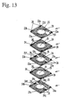
- Fig. 13 shows a laminate module according to the fourth embodiment of the present invention.
- This embodiment is a modification of the laminate module shown in Fig. 2, with the same reference numerals given to the same constituents. While only a load electrode 22c is connected through a via-electrode 26 in the embodiment shown in Fig. 2, all of capacitor electrodes 22a-24a on the input side, capacitor electrodes 22b-24b on the output side, load electrodes 22c-24c and ground electrodes 22d-24d, 22e-24e, 23f, 24f, 23g, 24g are connected through via-electrodes 26 in this embodiment.
- This structure simplifies a production process and thus shortens tact, resulting in lower production cost, than when the side-surface electrodes are used.
- the connection of electrode patterns is carried out with via-electrodes, side-surface electrodes, side through-holes, etc., and these connection means may be selected properly, considering their characteristics.
- Fig. 14 is a schematic block diagram showing a cellular phone as wireless communications equipment comprising the isolator of the present invention.
- the wireless communications equipment of this embodiment comprises an antenna 80, a duplexer 81 comprising a transmission filter and a reception filter, a transmission circuit 82 connected to an input/output means on the side of a transmission filter of the duplexer 81, and a reception circuit 83 connected to an input/output means on the side of a reception filter of the duplexer 81.
- the transmission circuit 82 comprises a filter 82a, a mixer 82b and a power amplifier 82c in this order from the transmission circuit side.
- a transmission signal is amplified by the power amplifier 82c and passes through the isolator 82d of the present invention and the transmission filter of the duplexer 81, followed by emission from the antenna 80.
- a reception signal is transmitted from the antenna 80 to the reception filter of the duplexer 81 and then to the reception circuit 83, where it is amplified by a low-noise amplifier 83a.
- a filter 83b After it passes through a filter 83b, it is mixed with a signal emitted from a base station and distributed by a splitter 85 from a voltage-controlled oscillator VCO 84 by the mixer 83c to be converted to an intermediate frequency.
- the reception signal flowing from the mixer 83c enters into a reception circuit via a filter 83d.
- the above structure is a mere example of the wireless communications equipment.
- the resin-conductor composite base has good flatness in a contact surface comprising external terminals, free from insufficient connection of the external terminals to the circuit board. Also, because there is no erosion by soldering, soldering operation is extremely easy and reliable. Further, the mounting of the non-reciprocal circuit device of the present invention necessitates only a small area of a circuit board, it can provide miniaturized, lightweight wireless communications equipment. Even when the wireless communications equipment such as a cellular phone drops, for instance, from a height of a human face to a floor, the isolator part does not suffer damage because of the resin-conductor composite base.
- the non-reciprocal circuit device of the present invention is easily miniaturized because matching capacitors are formed in the laminate module. Also, because the non-reciprocal circuit device of the present invention comprises a resin-conductor composite base or resin-conductor composite base having terminal electrodes connected to the input/output terminals and ground terminals of a laminate module in the same plane as the ground electrode, and integrally having external terminals for connecting the internal circuit of the laminate module to the external circuit, it has a small size, low loss and high reliability, and is easy to produce. With this non-reciprocal circuit device, a miniaturized, high-performance wireless communications equipment can be obtained.
Landscapes
- Non-Reversible Transmitting Devices (AREA)
Applications Claiming Priority (2)
| Application Number | Priority Date | Filing Date | Title |
|---|---|---|---|
| JP2000086166 | 2000-03-27 | ||
| JP2000086166 | 2000-03-27 |
Publications (1)
| Publication Number | Publication Date |
|---|---|
| EP1139486A1 true EP1139486A1 (fr) | 2001-10-04 |
Family
ID=18602379
Family Applications (1)
| Application Number | Title | Priority Date | Filing Date |
|---|---|---|---|
| EP01107516A Withdrawn EP1139486A1 (fr) | 2000-03-27 | 2001-03-26 | Dispositif non-réciproque et dispositif de communication l'incorporant |
Country Status (5)
| Country | Link |
|---|---|
| US (1) | US6731183B2 (fr) |
| EP (1) | EP1139486A1 (fr) |
| KR (1) | KR20010090579A (fr) |
| CN (1) | CN1249846C (fr) |
| TW (1) | TW554565B (fr) |
Cited By (3)
| Publication number | Priority date | Publication date | Assignee | Title |
|---|---|---|---|---|
| GB2370161A (en) * | 2000-07-07 | 2002-06-19 | Murata Manufacturing Co | Nonreciprocal circuit device with matching circuit |
| EP1309031A3 (fr) * | 2001-11-06 | 2003-10-29 | Murata Manufacturing Co., Ltd. | Dispositif de circuit non réciproque et appareil de communication |
| CN111129676A (zh) * | 2020-01-14 | 2020-05-08 | 中国电子科技集团公司第九研究所 | 一种提高环行器谐波抑制性能的方法及环行器 |
Families Citing this family (11)
| Publication number | Priority date | Publication date | Assignee | Title |
|---|---|---|---|---|
| US20030062193A1 (en) * | 2001-09-07 | 2003-04-03 | Jacob Thaysen | Flexible structure with integrated sensor/actuator |
| KR100457061B1 (ko) * | 2001-11-17 | 2004-11-18 | 케이에스엠 주식회사 | 아이솔레이터 |
| KR100703213B1 (ko) * | 2005-12-19 | 2007-04-06 | 삼성전기주식회사 | Rf 밸런스드 정합소자 |
| JP4656186B2 (ja) * | 2008-05-27 | 2011-03-23 | 株式会社村田製作所 | 非可逆回路素子及び複合電子部品の製造方法 |
| EP3001241B1 (fr) * | 2013-08-19 | 2018-05-23 | Huawei Technologies Co., Ltd. | Optoisolateur |
| WO2017010039A1 (fr) * | 2015-07-15 | 2017-01-19 | 日本電気株式会社 | Élément de circuit non réversible et dispositif de communication sans fil |
| US11081768B2 (en) * | 2019-05-24 | 2021-08-03 | Intel Corporation | Fabricating an RF filter on a semiconductor package using selective seeding |
| JP6939860B2 (ja) * | 2019-09-20 | 2021-09-22 | Tdk株式会社 | 非可逆回路素子 |
| CN111403878A (zh) * | 2020-03-27 | 2020-07-10 | 深圳市信维通信股份有限公司 | 贴片式环行器 |
| CN111403884A (zh) * | 2020-03-27 | 2020-07-10 | 深圳市信维通信股份有限公司 | 贴片式环形器的制作方法 |
| CN112635946A (zh) * | 2020-12-30 | 2021-04-09 | 广东大普通信技术有限公司 | 一种结构稳定的环形器 |
Citations (3)
| Publication number | Priority date | Publication date | Assignee | Title |
|---|---|---|---|---|
| EP0664573A1 (fr) * | 1993-06-30 | 1995-07-26 | Murata Manufacturing Co., Ltd. | Element de circuit non reciproque |
| EP0843375A1 (fr) * | 1996-11-14 | 1998-05-20 | Murata Manufacturing Co., Ltd. | Dispositif de circuit nonréciproque |
| JPH1155009A (ja) * | 1997-07-31 | 1999-02-26 | Hitachi Metals Ltd | 非可逆回路素子 |
Family Cites Families (5)
| Publication number | Priority date | Publication date | Assignee | Title |
|---|---|---|---|---|
| JPH02300738A (ja) * | 1989-05-16 | 1990-12-12 | Brother Ind Ltd | 画像記録装置 |
| US5774024A (en) * | 1993-04-02 | 1998-06-30 | Murata Manufacturing Co, Ltd. | Microwave non-reciprocal circuit element |
| JPH0955607A (ja) | 1995-08-11 | 1997-02-25 | Taiyo Yuden Co Ltd | 非可逆回路素子 |
| JPH1041706A (ja) * | 1996-07-26 | 1998-02-13 | Hitachi Metals Ltd | 非可逆回路素子 |
| JPH11205011A (ja) | 1997-11-11 | 1999-07-30 | Hitachi Metals Ltd | 集中定数型非可逆回路素子 |
-
2001
- 2001-03-26 EP EP01107516A patent/EP1139486A1/fr not_active Withdrawn
- 2001-03-26 US US09/816,115 patent/US6731183B2/en not_active Expired - Lifetime
- 2001-03-27 CN CNB01119264XA patent/CN1249846C/zh not_active Expired - Lifetime
- 2001-03-27 KR KR1020010015886A patent/KR20010090579A/ko not_active Withdrawn
- 2001-03-27 TW TW090107178A patent/TW554565B/zh not_active IP Right Cessation
Patent Citations (3)
| Publication number | Priority date | Publication date | Assignee | Title |
|---|---|---|---|---|
| EP0664573A1 (fr) * | 1993-06-30 | 1995-07-26 | Murata Manufacturing Co., Ltd. | Element de circuit non reciproque |
| EP0843375A1 (fr) * | 1996-11-14 | 1998-05-20 | Murata Manufacturing Co., Ltd. | Dispositif de circuit nonréciproque |
| JPH1155009A (ja) * | 1997-07-31 | 1999-02-26 | Hitachi Metals Ltd | 非可逆回路素子 |
Non-Patent Citations (1)
| Title |
|---|
| PATENT ABSTRACTS OF JAPAN vol. 1999, no. 05 31 May 1999 (1999-05-31) * |
Cited By (6)
| Publication number | Priority date | Publication date | Assignee | Title |
|---|---|---|---|---|
| GB2370161A (en) * | 2000-07-07 | 2002-06-19 | Murata Manufacturing Co | Nonreciprocal circuit device with matching circuit |
| US6522216B2 (en) | 2000-07-07 | 2003-02-18 | Murata Manufacturing Co., Ltd. | Nonreciprocal circuit device and communication apparatus |
| GB2370161B (en) * | 2000-07-07 | 2003-11-12 | Murata Manufacturing Co | Nonreciprocal circuit device and communication apparatus |
| EP1309031A3 (fr) * | 2001-11-06 | 2003-10-29 | Murata Manufacturing Co., Ltd. | Dispositif de circuit non réciproque et appareil de communication |
| US6734754B2 (en) | 2001-11-06 | 2004-05-11 | Murata Manufacturing Co., Ltd. | Nonreciprocal circuit device having a protruding electrode |
| CN111129676A (zh) * | 2020-01-14 | 2020-05-08 | 中国电子科技集团公司第九研究所 | 一种提高环行器谐波抑制性能的方法及环行器 |
Also Published As
| Publication number | Publication date |
|---|---|
| TW554565B (en) | 2003-09-21 |
| KR20010090579A (ko) | 2001-10-18 |
| CN1249846C (zh) | 2006-04-05 |
| US20020008596A1 (en) | 2002-01-24 |
| CN1318878A (zh) | 2001-10-24 |
| US6731183B2 (en) | 2004-05-04 |
Similar Documents
| Publication | Publication Date | Title |
|---|---|---|
| US6731183B2 (en) | Non-reciprocal circuit device and wireless communications equipment comprising same | |
| US7420435B2 (en) | Non-reciprocal circuit element, method for manufacturing the same, and communication device | |
| US6559732B2 (en) | Nonreciprocal circuit device with main surfaces of the ferrite and magnet perpendicular to the mounting substrate | |
| US8134422B2 (en) | Non-reciprocal circuit device | |
| US6992540B2 (en) | Two-port isolator and communication device | |
| US7432777B2 (en) | Non-reciprocal circuit element, composite electronic component, and communication apparatus | |
| JP4345709B2 (ja) | 非可逆回路素子、その製造方法及び通信装置 | |
| US8525610B2 (en) | Composite electronic module and method of manufacturing composite electronic module | |
| US6850751B1 (en) | Non-reciprocal circuit device, method of manufacturing, and mobile communication apparatus using the same | |
| JP4517326B2 (ja) | 非可逆回路素子及びこれを用いた無線通信機器 | |
| EP1309031B1 (fr) | Dispositif de circuit non réciproque et appareil de communication | |
| KR100397740B1 (ko) | 비가역 회로소자 및 통신 장치 | |
| US6906597B2 (en) | Non-reciprocal circuit device and resin casing used therefor | |
| JPH11239009A (ja) | 非可逆回路素子の広帯域化構造 | |
| US6724276B2 (en) | Non-reciprocal circuit device and communication apparatus | |
| US7394330B2 (en) | Non-reciprocal circuit element | |
| JP2004356745A (ja) | 非可逆回路素子 | |
| JP4208087B2 (ja) | 非可逆回路素子及び通信機器 | |
| US20080111648A1 (en) | Non-reciprocal circuit element, composite electronic component, and communication apparatus | |
| JP4066333B2 (ja) | 非可逆回路素子 | |
| JP4780311B2 (ja) | 非可逆回路素子、及び、これを用いた通信機器 | |
| JP3714220B2 (ja) | 非可逆回路素子及び通信装置 | |
| JP2002185216A (ja) | 非可逆回路素子 | |
| JP2002271110A (ja) | 非可逆回路素子及び通信装置 | |
| JP2005033366A (ja) | 非可逆回路素子及び通信機装置 |
Legal Events
| Date | Code | Title | Description |
|---|---|---|---|
| PUAI | Public reference made under article 153(3) epc to a published international application that has entered the european phase |
Free format text: ORIGINAL CODE: 0009012 |
|
| AK | Designated contracting states |
Kind code of ref document: A1 Designated state(s): AT BE CH CY DE DK ES FI FR GB GR IE IT LI LU MC NL PT SE TR |
|
| AX | Request for extension of the european patent |
Free format text: AL;LT;LV;MK;RO;SI |
|
| 17P | Request for examination filed |
Effective date: 20020402 |
|
| AKX | Designation fees paid |
Free format text: AT BE CH CY DE DK ES FI FR GB GR IE IT LI LU MC NL PT SE TR |
|
| 17Q | First examination report despatched |
Effective date: 20020731 |
|
| GRAP | Despatch of communication of intention to grant a patent |
Free format text: ORIGINAL CODE: EPIDOSNIGR1 |
|
| STAA | Information on the status of an ep patent application or granted ep patent |
Free format text: STATUS: THE APPLICATION IS DEEMED TO BE WITHDRAWN |
|
| 18D | Application deemed to be withdrawn |
Effective date: 20050517 |