EP1143404A2 - Verfahren und Einrichtung zur Anzeige von Bildern - Google Patents
Verfahren und Einrichtung zur Anzeige von Bildern Download PDFInfo
- Publication number
- EP1143404A2 EP1143404A2 EP01301290A EP01301290A EP1143404A2 EP 1143404 A2 EP1143404 A2 EP 1143404A2 EP 01301290 A EP01301290 A EP 01301290A EP 01301290 A EP01301290 A EP 01301290A EP 1143404 A2 EP1143404 A2 EP 1143404A2
- Authority
- EP
- European Patent Office
- Prior art keywords
- display
- cell
- cells
- image
- light emission
- Prior art date
- Legal status (The legal status is an assumption and is not a legal conclusion. Google has not performed a legal analysis and makes no representation as to the accuracy of the status listed.)
- Granted
Links
Images


Classifications
-
- G—PHYSICS
- G09—EDUCATION; CRYPTOGRAPHY; DISPLAY; ADVERTISING; SEALS
- G09G—ARRANGEMENTS OR CIRCUITS FOR CONTROL OF INDICATING DEVICES USING STATIC MEANS TO PRESENT VARIABLE INFORMATION
- G09G3/00—Control arrangements or circuits, of interest only in connection with visual indicators other than cathode-ray tubes
- G09G3/20—Control arrangements or circuits, of interest only in connection with visual indicators other than cathode-ray tubes for presentation of an assembly of a number of characters, e.g. a page, by composing the assembly by combination of individual elements arranged in a matrix no fixed position being assigned to or needed to be assigned to the individual characters or partial characters
- G09G3/22—Control arrangements or circuits, of interest only in connection with visual indicators other than cathode-ray tubes for presentation of an assembly of a number of characters, e.g. a page, by composing the assembly by combination of individual elements arranged in a matrix no fixed position being assigned to or needed to be assigned to the individual characters or partial characters using controlled light sources
- G09G3/28—Control arrangements or circuits, of interest only in connection with visual indicators other than cathode-ray tubes for presentation of an assembly of a number of characters, e.g. a page, by composing the assembly by combination of individual elements arranged in a matrix no fixed position being assigned to or needed to be assigned to the individual characters or partial characters using controlled light sources using luminous gas-discharge panels, e.g. plasma panels
- G09G3/288—Control arrangements or circuits, of interest only in connection with visual indicators other than cathode-ray tubes for presentation of an assembly of a number of characters, e.g. a page, by composing the assembly by combination of individual elements arranged in a matrix no fixed position being assigned to or needed to be assigned to the individual characters or partial characters using controlled light sources using luminous gas-discharge panels, e.g. plasma panels using AC panels
- G09G3/291—Control arrangements or circuits, of interest only in connection with visual indicators other than cathode-ray tubes for presentation of an assembly of a number of characters, e.g. a page, by composing the assembly by combination of individual elements arranged in a matrix no fixed position being assigned to or needed to be assigned to the individual characters or partial characters using controlled light sources using luminous gas-discharge panels, e.g. plasma panels using AC panels controlling the gas discharge to control a cell condition, e.g. by means of specific pulse shapes
-
- G—PHYSICS
- G09—EDUCATION; CRYPTOGRAPHY; DISPLAY; ADVERTISING; SEALS
- G09G—ARRANGEMENTS OR CIRCUITS FOR CONTROL OF INDICATING DEVICES USING STATIC MEANS TO PRESENT VARIABLE INFORMATION
- G09G3/00—Control arrangements or circuits, of interest only in connection with visual indicators other than cathode-ray tubes
- G09G3/20—Control arrangements or circuits, of interest only in connection with visual indicators other than cathode-ray tubes for presentation of an assembly of a number of characters, e.g. a page, by composing the assembly by combination of individual elements arranged in a matrix no fixed position being assigned to or needed to be assigned to the individual characters or partial characters
- G09G3/22—Control arrangements or circuits, of interest only in connection with visual indicators other than cathode-ray tubes for presentation of an assembly of a number of characters, e.g. a page, by composing the assembly by combination of individual elements arranged in a matrix no fixed position being assigned to or needed to be assigned to the individual characters or partial characters using controlled light sources
- G09G3/28—Control arrangements or circuits, of interest only in connection with visual indicators other than cathode-ray tubes for presentation of an assembly of a number of characters, e.g. a page, by composing the assembly by combination of individual elements arranged in a matrix no fixed position being assigned to or needed to be assigned to the individual characters or partial characters using controlled light sources using luminous gas-discharge panels, e.g. plasma panels
- G09G3/288—Control arrangements or circuits, of interest only in connection with visual indicators other than cathode-ray tubes for presentation of an assembly of a number of characters, e.g. a page, by composing the assembly by combination of individual elements arranged in a matrix no fixed position being assigned to or needed to be assigned to the individual characters or partial characters using controlled light sources using luminous gas-discharge panels, e.g. plasma panels using AC panels
- G09G3/298—Control arrangements or circuits, of interest only in connection with visual indicators other than cathode-ray tubes for presentation of an assembly of a number of characters, e.g. a page, by composing the assembly by combination of individual elements arranged in a matrix no fixed position being assigned to or needed to be assigned to the individual characters or partial characters using controlled light sources using luminous gas-discharge panels, e.g. plasma panels using AC panels using surface discharge panels
- G09G3/2983—Control arrangements or circuits, of interest only in connection with visual indicators other than cathode-ray tubes for presentation of an assembly of a number of characters, e.g. a page, by composing the assembly by combination of individual elements arranged in a matrix no fixed position being assigned to or needed to be assigned to the individual characters or partial characters using controlled light sources using luminous gas-discharge panels, e.g. plasma panels using AC panels using surface discharge panels using non-standard pixel electrode arrangements
-
- G—PHYSICS
- G09—EDUCATION; CRYPTOGRAPHY; DISPLAY; ADVERTISING; SEALS
- G09G—ARRANGEMENTS OR CIRCUITS FOR CONTROL OF INDICATING DEVICES USING STATIC MEANS TO PRESENT VARIABLE INFORMATION
- G09G3/00—Control arrangements or circuits, of interest only in connection with visual indicators other than cathode-ray tubes
- G09G3/20—Control arrangements or circuits, of interest only in connection with visual indicators other than cathode-ray tubes for presentation of an assembly of a number of characters, e.g. a page, by composing the assembly by combination of individual elements arranged in a matrix no fixed position being assigned to or needed to be assigned to the individual characters or partial characters
- G09G3/22—Control arrangements or circuits, of interest only in connection with visual indicators other than cathode-ray tubes for presentation of an assembly of a number of characters, e.g. a page, by composing the assembly by combination of individual elements arranged in a matrix no fixed position being assigned to or needed to be assigned to the individual characters or partial characters using controlled light sources
- G09G3/28—Control arrangements or circuits, of interest only in connection with visual indicators other than cathode-ray tubes for presentation of an assembly of a number of characters, e.g. a page, by composing the assembly by combination of individual elements arranged in a matrix no fixed position being assigned to or needed to be assigned to the individual characters or partial characters using controlled light sources using luminous gas-discharge panels, e.g. plasma panels
- G09G3/288—Control arrangements or circuits, of interest only in connection with visual indicators other than cathode-ray tubes for presentation of an assembly of a number of characters, e.g. a page, by composing the assembly by combination of individual elements arranged in a matrix no fixed position being assigned to or needed to be assigned to the individual characters or partial characters using controlled light sources using luminous gas-discharge panels, e.g. plasma panels using AC panels
- G09G3/298—Control arrangements or circuits, of interest only in connection with visual indicators other than cathode-ray tubes for presentation of an assembly of a number of characters, e.g. a page, by composing the assembly by combination of individual elements arranged in a matrix no fixed position being assigned to or needed to be assigned to the individual characters or partial characters using controlled light sources using luminous gas-discharge panels, e.g. plasma panels using AC panels using surface discharge panels
- G09G3/299—Control arrangements or circuits, of interest only in connection with visual indicators other than cathode-ray tubes for presentation of an assembly of a number of characters, e.g. a page, by composing the assembly by combination of individual elements arranged in a matrix no fixed position being assigned to or needed to be assigned to the individual characters or partial characters using controlled light sources using luminous gas-discharge panels, e.g. plasma panels using AC panels using surface discharge panels using alternate lighting of surface-type panels
-
- G—PHYSICS
- G09—EDUCATION; CRYPTOGRAPHY; DISPLAY; ADVERTISING; SEALS
- G09G—ARRANGEMENTS OR CIRCUITS FOR CONTROL OF INDICATING DEVICES USING STATIC MEANS TO PRESENT VARIABLE INFORMATION
- G09G2310/00—Command of the display device
- G09G2310/02—Addressing, scanning or driving the display screen or processing steps related thereto
- G09G2310/0224—Details of interlacing
Definitions
- the present invention relates to a method and an apparatus for displaying an image, which are suitable especially for a display using a plasma display panel (PDP).
- PDP plasma display panel
- an AC type PDP of a surface discharge format As a television display device having a large screen, an AC type PDP of a surface discharge format is commercialized.
- the surface discharge format has first and second display electrodes each of which serves as an anode or a cathode in a display discharge for ensuring a luminance arranged in parallel on a front or a back substrate.
- a "three-electrode structure" is widely known, in which an address electrode is arranged so as to cross the display electrode pair.
- one of the display electrodes (the second display electrode) is used as a scanning electrode for selecting a display line, and an address discharge is generated between the scanning electrode and the address electrode so as to control the wall charge in accordance with the content of the display for addressing.
- a sustaining voltage having an alternating polarity is applied to the display electrodes, so that a surface discharge is generated only in the cell having a predetermined wall charge along the substrate surface.
- a partition for dividing a discharge space into columns is necessary.
- a stripe structure in which a partition having a banding shape in the plan view is arranged (including a structure in which a stripe pattern layer and a mesh pattern layer are overlaid) has an advantage over a mesh (waffle) structure in which each cell is separated from others.
- the discharge space of each column is continuous over the entire length of the screen, so that a discharge probability is increased by a priming effect, and that a fluorescent material layer can be arranged uniformly and easily, and that an air exhaustion process can be shortened.
- Japanese unexamined patent publication No. 9-160525 discloses a three-electrode surface discharge type PDP that is used for an interlaced display.
- display electrodes are arranged at a constant pitch so as to be connected with all columns that are defined by linear banding partitions, and the number of the display electrodes equals the number N of the display linesin the screen plus one.
- the (N+1) display electrodes two neighboring display electrodes constitute an electrode pair for generating a surface discharge and define one display line (row) of the screen.
- Each of the display electrodes except for both ends of the arrangement works for two display lines (an odd display line and an even display line), while each of the end display electrodes works for one display line.
- the PDP wherein all display electrode gaps are made discharge gaps and one display electrode is shared by two display lines for discharge, has an advantage in that the resolution (the number of display lines) is substantially doubled, and that there is no non-light emission area between the display lines so that each cell a large aperture ratio, compared with a PDP in which a pair of display electrodes is arranged for each display line.
- each partition meanders so as to form a column space having alternating widened portions and narrowed portions in cooperation with the neighboring partition. The position of the widened portion in which a cell is formed is shifted from that of the neighboring column, so that the arrangement of three colors for a color display becomes Delta Tricolor Arrangement.
- each display line is made of cells including a fixed cell selected for each column.
- the display line pitch equals the cell arrangement pitch in the column direction, so there is a problem in that it is necessary to reduce the cell size in order to improve the resolution in the column direction.
- a method of displaying an image comprises the steps of using a display device having a display surface including plural cell columns each of which is a set of cells having the same light emission color, the display device having a cell arrangement structure in which cell positions in the column direction are shifted from each other between the neighboring cell columns, and performing an interlaced display by changing the combination of cells of a display line that is perpendicular to the column direction in every field between the neighboring cell columns of the same light emission color.
- the method may further comprise the step of determining luminance of each cell of the display surface by distributing a luminance value of each pixel of an input image to be displayed to cells corresponding to pixels in accordance with the cell position relationship between a virtual display surface having a cell arrangement corresponding to a pixel arrangement of the input image and the display surface.
- a display apparatus comprising a display device having a display surface including plural cell columns each of which is a set of cells having the same light emission color, the display device having a cell arrangement structure in which cell positions in the column direction are shifted from each other between the neighboring cell columns, and a driving circuit for performing an interlaced display by changing the combination of cells of a display line that is perpendicular to the column direction in every field between the neighboring cell columns of the same light emission color in every field.
- the display apparatus may have a structure in which the cells are arranged at a constant pitch in each cell column and the shift quantity of the cell position in the column direction between the neighboring cell columns of the same light emission color is a half of the cell arrangement pitch.
- the display apparatus may have a structure in which luminance of each cell of the display surface is determined by distributing a luminance value of each pixel of an input image to be displayed to cells corresponding to pixels in accordance with the cell position relationship between a virtual display surface having a cell arrangement corresponding to a pixel arrangement of the input image and the display surface.
- the display apparatus may have a structure in which all cells within the display surface have the same light emission color.
- the display apparatus may have a structure in which the display surface includes three kinds of cell columns having different light emission colors, and the color arrangement has a pattern in which three colors are repeated in the same order.
- the display apparatus may have a structure in which an interlaced image to be displayed is inputted, and the direction of the display line is the direction of a scanning line of the interlaced image.
- the display apparatus may have a structure in which a non-interlaced image to be displayed is inputted, and the non-interlaced image is converted into an interlaced image to be displayed.
- the display apparatus may have a structure in which gradation data of each pixel of the interlaced image are generated from the non-interlaced image data.
- the display apparatus may include a plasma display panel as the display device.
- the display device may be a plasma display panel having an inner structure including a partition for dividing a discharge space for each cell column, the discharge space may be continuous over the entire length of the display surface in each cell column, and wide portions and narrow portions may be arranged alternately so that the narrow portion is located at the boundary position between cells.
- the display device may have a plurality of scanning electrodes arranged to straddle over all cell columns for selecting one cell in each cell column of each field.
- Fig. 1 is a block diagram of a display apparatus according to the present invention.
- the display apparatus 100 comprises a three-electrode surface discharge type PDP 1 and a drive unit 70 for selectively activating a cell arranged in a matrix to emit light.
- the display apparatus 100 is used as a wall-hung TV set or a monitor display of a computer system.
- the PDP 1 has a display electrode X and a display electrode Y extending in the display line direction (i.e., in the horizontal direction).
- the display electrode Y is used as a scanning electrode for addressing.
- the address electrode A extends in the column direction (in the vertical direction).
- the drive unit 70 includes a control circuit 71 for a drive control, a power source circuit 73, an X driver 74, a Y driver 77, and an address driver 80.
- the drive unit 70 is supplied with frame data Df that are multivalued image data indicating luminance levels of red, green and blue colors along with various synchronizing signals from external equipment such as a TV tuner or a computer.
- the control circuit 71 includes a frame memory 711 for memorizing the frame data Df temporarily and a waveform memory 712 for memorizing control data of drive voltages. As known widely, a display using a PDP reproduces gradation by controlling lighting in a binary manner.
- each of sequential frames of an input image or a field of the frame is divided into plural subfield.
- a subfield period that is assigned to each subfield includes a preparation period for equalize a charge distribution of the display surface, an address period for forming a charge distribution corresponding to a display content, and a sustaining period for generating a display discharge for ensuring a luminance level corresponding to a gradation level.
- a ramp pulse is applied to adjust a wall voltage to a desired value, for example.
- a scan pulse is applied to the display electrode Y for selecting a display line, and, in synchronization with that, the potential of the address electrode A is controlled in binary manner for addressing.
- a sustaining pulse is applied to the display electrode Y and the display electrode X alternately.
- a peak value of the sustaining pulse is lower than a discharge start voltage between the display electrodes, so the surface discharge does not occur without the wall voltage being added. Only the lighted cell in which the wall charge was formed during the address period can generate a surface discharge as the display discharge at every application of the sustaining pulse.
- the frame data Df are stored in the frame memory 711 temporarily and then are converted into subfield data Dsf for the gradation display, which are transferred to the address driver 80.
- the subfield data Dsf are display data made of q bits corresponding to q subfields (a set of display data for q screens in which one bit indicates one subpixel), and the subfield is a binary image.
- the value of each bit of the subfield data Dsf indicates whether the subpixel of the corresponding subfield is to be lighted or not, more accurately, whether it requires the address discharge or not.
- the X driver 74 controls the potential of all display electrodes X as a whole.
- the Y driver 77 includes a scan circuit 78 for addressing and a common driver 79 for sustaining.
- the scan circuit 78 is means for applying a scan pulse to select a display line.
- the address driver 80 controls potentials of M address electrodes A in accordance with the subfield data Dsf. These drivers are supplied with a predetermined power via wiring conductors (not shown) from the power source circuit 73.
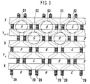
- Fig. 2 is a diagram showing a cell structure of a PDP according to the present invention.
- Fig. 3 is a plan view showing a cell arrangement structure.
- the inner structure is shown by drawing a pair of substrate structures in a separated state.
- the display electrode Y whose potential can be controlled individually, is denoted by the reference character "Y" with a suffix indicating an arrangement order.
- the PDP 1 includes a pair of substrate structures (each substrate structure has a substrate on which elements of discharge cells are arranged) 10 and 20.
- the display electrodes X and Y are arranged on the inner surface of the front glass substrate 11.
- Each of the display electrodes X and Y includes a transparent conductive film 41 for forming a surface discharge gap and a metal film (a bus electrode) 42 extending in the horizontal direction over the entire length of the display surface ES.
- the display electrodes X and Y are coated with a dielectric layer 17, which is coated with magnesia (MgO) as a protection film 18.
- the address electrode A is arranged on the inner surface of the back glass substrate 21 and covered with a dielectric layer 24.
- meandering band-like partitions 29 each having a height of approximately 150 ⁇ m are arranged for dividing the discharge space into columns.
- a column space 31 of the discharge space corresponding to each column is continuous over all display lines.
- the back inner surface and the side face of the partition 29 are covered with fluorescent material layers 28R, 28G and 28B of red, green and blue colors for a color display.
- Italic letters R, G and B in the figure denote light emission colors of fluorescent materials (ditto for the following figures). The color arrangement of red, blue and green pattern is repeated.
- the fluorescent material layers 28R, 28G and 28B are excited locally by ultraviolet rays generated by the discharge gas and emit light.
- the neighboring partitions form a column space 31 including wide portions and narrow portions that are alternating.
- the position of the wide portion in the column direction is shifted from that of the neighboring column by one-half of a cell pitch in the column direction.
- a cell as a display element is formed in each wide portion.
- Cells 51, 52 and 53 of one line are indicated by chain-lined circle as representatives in the figure.
- the display line is a set of cells that are lighted for displaying a line having the minimum width in the horizontal direction.
- the cells 51, 52 and 53 of three columns are used for reproduce a color of a pixel of an input image.
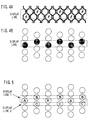
- Figs. 4A and 4B show a layout in which the relationship between positions of cells having the same light emission color of one display line is indicated.
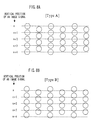
- Fig. 5 shows a set of display lines according to the present invention.
- a resolution in the column direction can be improved by utilizing the characteristic that the cell position in the column direction is shifted from that of the neighboring column. It is because display lines that are shifted from each other by half a pitch by changing the combination of cells. As shown in Fig. 5, the position of the display line 1 including the cell A and the cell B is shifted from the position of the display line 2 including the cell A and the cell C by half a pitch.
- the display line 1 when the structure of the display line 1 is adopted for even fields, and when the structure of the display line 2 is adopted for odd fields, the display line is shifted by half a pitch for every field, so that an interlaced display of image information having a display line number that is twice the scanning electrode number.
- a gradation level of a cell of a certain color is C n,m .
- the suffix n denotes the position in the vertical direction
- the suffix m denotes the position in the horizontal direction, as defined in Figs. 6 and 7. It should be noted that the numbering of the position depends on the color.
- the position in the vertical direction of the odd cell in the horizontal direction is shifted from that of the even cell by half a cell pitch in the vertical direction (a pitch of the scanning electrode in this example).
- the interlaced image signal corresponding to the cell of the noted color is denoted by T n,m .
- the signal of an even field is denoted by T 2n,m while the signal of an odd field is denoted by T 2n+1,m .
- the cells having vertical positions of 2n and 2n+1 are assigned to the same display line (horizontal line) for an even field, while the cells having vertical positions of 2n and 2n-1 are assigned to the same display line for an odd field.
- the relationship between the gradation level and the signal for the red or blue light emission color is defined by the following equations.
- one line of the image signal corresponds to one scanning electrode as-is for an even field. Therefore, address data (subfield data) can be generated in the order of the image signal. However, concerning an odd field, one line of the image signal straddles two scanning electrodes. Therefore, address data corresponding to one scanning electrode are generated in accordance with the data of the image signal that is shifted in the vertical direction by a line depending on which the horizontal position is even or odd.
- the image data S n,m of the cell corresponding to the n-th scanning electrode for a cell having the red or blue light emission color are defined by the following equations.
- the image data S n,m of the cell corresponding to the n-th scanning electrode for a cell having the green light emission color are defined by the following equations.
- an interlaced image information display having display lines whose number is twice the number of scanning electrodes can be performed. It is not necessary that the number of display lines of the image information is equal to the number of scanning electrodes.
- An appropriate format conversion enables a non-interlace (progressive) image information display having display lines more than scanning electrodes. Next, an example of the conversion from non-interlaced image information to interlaced image information.
- P n,m denotes non-interlaced image information.
- V p denotes a vertical pitch of the image information
- Hp denotes a horizontal pitch.
- V d denotes one-half of a scanning electrode pitch of the PDP 1
- H d denotes a horizontal pitch.
- the image information can be obtained with any pitch in the horizontal direction.
- the position of the image information in the horizontal direction is defined in a digital signal.
- indexes of pixels start from zero both in the vertical direction and in the horizontal direction. An edge of the pixel having the index of zero is assigned to the origin of coordinates.
- a conversion in the horizontal direction is considered.
- the m-th pixel occupies the space position from mH d to (m+1)H d on the display surface.
- the value of display is an average value of pixels of the image information within the above-mentioned range. Concerning a pixel whose pixel area is not completely in the range, the value is calculated by prorating.
- P' n,m denotes image information after converting the format only in the horizontal direction.
- the conversion rule is as following equation.
- the interlaced display is performed in accordance with the equations (1)-(4).
- the data conversion means are not limited to means that generate the data C n,m of the cell directly from the input image data P n,m .
- Means for generating the interlaced signal T n,m from the image data P n,m can be separated from means for generating the data C n,m from the interlaced signal. Such a separation facilitates support of various signals only by changing the means for generating the interlaced signal.
- Example 2 the method of converting an image signal defined in the general equation into an interlaced signal is explained.
- the conversion of a signal is usually performed between the formats in which the pixel pitches are defined by a simple integer ratio.
- Example 3 a conversion rule in the case where the pixel pitches are defined by an integer ratio will be explained.
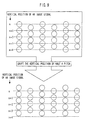
- Type A is the case where the period boundary is at the edge of the cell as shown in Fig. 8A
- Type B is the case where the period boundary is at the center of the cell as shown in Fig. 8B. Therefore, four combinations of conversion rules are considered.
- the edges of the image areas of two formats are not completely identical except for the conversion from Type A into Type A. Therefore, a special process is necessary at the edge portion for the conversion, resulting in an excess job. Accordingly, the conversion from Type A to Type A is practical.
- the conversion rule in this case is the same as in Example 2.
- the practical conversion that is the most important at the present time is the conversion from a 1280 x 720 non-interlaced signal that is a standard of a digital TV into a 1920 x 1080 interlaced signal.
- the pixel pitch is three to two.
- the concrete conversion rule is defined by the following equation.
- 540 of scanning electrodes enable displaying an interlaced image having 1080 lines and a non-interlaced image having 720 lines.
- the non-interlaced image When displaying a non-interlaced image having display lines whose number is the same as the number of scanning electrodes, unevenness of the display lines that is unique to the delta arrangement becomes conspicuous if the combination of cells of the display line is fixed. In order to avoid this problem, the non-interlaced image is converted into an interlaced image having the number of lines twice the number of scanning electrodes, so as to perform the interlaced display.
- P n,m denotes the image information of the non-interlace.
- the pitch of the vertical direction is the same as the pitch of the scanning electrodes.
- the image information is converted into the interlaced image information T n,m in which the number of lines is doubled.
- One of the methods is to distribute the luminance value of the pixel of the image data to plural cells considering the cell position of the display surface.
- the luminance of each cell is determined as follows.
- the gradation level of a certain cell is denoted by C n,m .
- the suffix "n” indicates the vertical position
- the suffix "m” indicates the horizontal position as shown in Figs. 6 and 7.
- the image signal corresponding to the cell of the noted color is denoted by T n,m .
- the vertical position of the horizontal line of the image signal is considered as Type A or Type B from the viewpoint of symmetry.
- Type A vertical position is the same as the cell.
- type B the vertical position is the center position between cells.
- the display that is faithful to the position information of the image data can be realized, so that the display quality of the horizontal line can be improved.
- Example 5 the vertical position of the horizontal line of the input image can be shifted by a half pitch of the scanning electrode pitch.
- Application of this method to Type A is shown in Fig. 9.
- the relationship between the image signal and the display luminance of the cell when the vertical position is shifted is defined by the following equations.
- T n,m denotes information of an interlaced image.
- T' 2n,m denotes information of an even field, and T' 2n,m denotes information of an odd field.
- the relationship between the image signal and the display luminance of a cell is defined by the following equations.
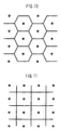
- Fig. 10 shows a unit display area of a certain color and the display center thereof.
- the display center indicated by a dot in Fig. 10 is the cell center.
- the unit display area means an image area to be displayed by the cell. More specifically, the area is divided so that a certain position on the image is included in the unit display area to which the closest display center belongs.
- a hexagonal area surrounding the display center in Fig. 10 is the unit display area.
- the border line passes the center of the line that connects display centers facing each other with respect to the border line and is perpendicular to the line.
- the "unit information area” means the area where the image is expressed with discrete image information.
- the area is usually divided with rectangles.
- the information center signifies a position of the discrete information.
- the information in a unit area of the image is assigned to the center of the information.
- the individual image information unit represents image information of the unit information area. Therefore, the distribution of the information should be performed in accordance with the area ratio where the individual unit display area is overlaid on the noted unit information area.
- Fig. 12A The type of overlay of the unit information area with the unit display area in Type A is shown in Fig. 12A, and that in Type B is shown in Fig. 12B.
- Solid lines indicate boundaries between unit display areas, and broken lines indicate boundaries between unit information areas.
- Type A including a shift of a half pitch is defined by the following equations.
- Type B is defined by the following equations.
- Type B including a shift of a half pitch is defined by the following equations.
- an image can be displayed more faithfully concerning position information. It is possible to apply the method of distributing image information to each cell in accordance with the overlaying area ratio of the unit information area of each color with the unit display area to the case where the image information has any pitch in the horizontal direction as well as in the vertical direction. Furthermore, in the case of Example 5 or 6, it can be considered that the image information is divided by the overlaying area ratio of the unit information area of each color with the unit display area after making approximation of the unit display area as shown in Fig. 13.
- the present invention can be applied to any display devices other than a PDP if the cell arrangement is similar.
- the display is not limited to a color display, but can be a monochromatic display using a device in which all cells emit light of the same color.
- a high definition display can be realized in which the display line pitch is smaller than the cell arrangement pitch in the column direction in the display surface having display lines of cells arranged zigzag.
- a high definition display can be realized that has a large aperture ratio of a cell, high luminance, low possibility of cross talk in the column direction and little display fluctuations, and in which the display line pitch is smaller than the cell arrangement pitch in the column direction.
Landscapes
- Engineering & Computer Science (AREA)
- Physics & Mathematics (AREA)
- Power Engineering (AREA)
- Plasma & Fusion (AREA)
- Computer Hardware Design (AREA)
- General Physics & Mathematics (AREA)
- Theoretical Computer Science (AREA)
- Control Of Indicators Other Than Cathode Ray Tubes (AREA)
- Control Of Gas Discharge Display Tubes (AREA)
- Gas-Filled Discharge Tubes (AREA)
- Transforming Electric Information Into Light Information (AREA)
- Devices For Indicating Variable Information By Combining Individual Elements (AREA)
Applications Claiming Priority (2)
| Application Number | Priority Date | Filing Date | Title |
|---|---|---|---|
| JP2000105897 | 2000-04-07 | ||
| JP2000105897A JP4158874B2 (ja) | 2000-04-07 | 2000-04-07 | 画像表示方法および表示装置 |
Publications (3)
| Publication Number | Publication Date |
|---|---|
| EP1143404A2 true EP1143404A2 (de) | 2001-10-10 |
| EP1143404A3 EP1143404A3 (de) | 2005-01-12 |
| EP1143404B1 EP1143404B1 (de) | 2008-09-10 |
Family
ID=18619154
Family Applications (1)
| Application Number | Title | Priority Date | Filing Date |
|---|---|---|---|
| EP01301290A Expired - Lifetime EP1143404B1 (de) | 2000-04-07 | 2001-02-13 | Verfahren und Einrichtung zur Anzeige von Bildern |
Country Status (5)
| Country | Link |
|---|---|
| US (1) | US7050021B2 (de) |
| EP (1) | EP1143404B1 (de) |
| JP (1) | JP4158874B2 (de) |
| KR (1) | KR100778813B1 (de) |
| DE (1) | DE60135701D1 (de) |
Cited By (5)
| Publication number | Priority date | Publication date | Assignee | Title |
|---|---|---|---|---|
| US6825835B2 (en) | 2000-11-24 | 2004-11-30 | Mitsubishi Denki Kabushiki Kaisha | Display device |
| EP1345115A3 (de) * | 2002-03-15 | 2005-12-14 | Fujitsu Limited | Daten-Umwandlungsschaltung und Farbbildanzeigevorrichtung |
| EP1282105A3 (de) * | 2001-07-31 | 2007-12-05 | Hitachi Plasma Patent Licensing Co., Ltd. | Verfahren zur Anzeige von Farbbildern |
| EP1376525A3 (de) * | 2002-06-21 | 2008-04-09 | Hitachi Plasma Patent Licensing Co., Ltd. | Plasmabildanzeigevorrichtung und Steuerungsverfahren dafür |
| EP1870921A3 (de) * | 2006-06-21 | 2010-01-20 | Samsung SDI Co., Ltd. | Plasmaanzeigetafel |
Families Citing this family (20)
| Publication number | Priority date | Publication date | Assignee | Title |
|---|---|---|---|---|
| JP4269133B2 (ja) * | 2001-06-29 | 2009-05-27 | 株式会社日立プラズマパテントライセンシング | Ac型pdpの駆動装置および表示装置 |
| KR100489445B1 (ko) * | 2001-11-29 | 2005-05-17 | 엘지전자 주식회사 | 플라즈마 표시 패널의 구동방법 |
| WO2003079392A2 (en) * | 2002-03-19 | 2003-09-25 | Koninklijke Philips Electronics N.V. | Plasma display panel electrode and phosphor structure |
| KR100480168B1 (ko) * | 2002-05-31 | 2005-04-06 | 엘지전자 주식회사 | 플라즈마 디스플레이 패널의 구동방법 |
| JP3948557B2 (ja) * | 2002-06-28 | 2007-07-25 | 株式会社日立プラズマパテントライセンシング | Pdp用のパネルアセンブリ及びその製造方法 |
| KR100482339B1 (ko) * | 2002-09-12 | 2005-04-13 | 엘지전자 주식회사 | 플라즈마 디스플레이 패널의 구동방법 |
| KR100502910B1 (ko) * | 2003-01-22 | 2005-07-21 | 삼성에스디아이 주식회사 | 델타 화소 배열 구조를 갖는 플라즈마 디스플레이 패널 |
| KR100477994B1 (ko) * | 2003-03-18 | 2005-03-23 | 삼성에스디아이 주식회사 | 플라즈마 디스플레이 패널 및 그 구동 방법 |
| FR2855646A1 (fr) * | 2003-05-26 | 2004-12-03 | Thomson Plasma | Panneau de visualisation a plasma a zone d'expansion de decharge de section reduite |
| US20050122291A1 (en) * | 2003-12-04 | 2005-06-09 | May Gregory J. | Optically addressable pixel and receptacle array |
| TWI282106B (en) * | 2003-12-23 | 2007-06-01 | Au Optronics Corp | Plasma display panel |
| JP4777675B2 (ja) * | 2005-03-17 | 2011-09-21 | 株式会社リコー | 画像処理装置、画像表示装置、画像処理方法、その方法をコンピュータに実行させるプログラム、および記録媒体 |
| KR100739056B1 (ko) * | 2005-11-23 | 2007-07-12 | 삼성에스디아이 주식회사 | 플라즈마 디스플레이 패널 및 그 제조 방법 |
| KR100786866B1 (ko) * | 2005-11-24 | 2007-12-20 | 삼성에스디아이 주식회사 | 플라즈마 디스플레이 패널 |
| KR100816199B1 (ko) * | 2005-11-30 | 2008-03-21 | 삼성에스디아이 주식회사 | 플라즈마 디스플레이 패널 및 그 제조방법 |
| KR100760765B1 (ko) * | 2005-11-30 | 2007-09-21 | 삼성에스디아이 주식회사 | 플라즈마 디스플레이 패널 |
| KR100759409B1 (ko) * | 2005-11-30 | 2007-09-19 | 삼성에스디아이 주식회사 | 플라즈마 디스플레이 패널 |
| KR100778516B1 (ko) * | 2006-06-01 | 2007-11-22 | 삼성에스디아이 주식회사 | 표시 장치 및 그 구동 방법 |
| KR100826191B1 (ko) * | 2006-06-29 | 2008-04-30 | 엘지전자 주식회사 | 평판 디스플레이의 고해상도 인터레이스 스캔 방법 및 그평판 디스플레이 장치 |
| KR100900061B1 (ko) * | 2007-12-10 | 2009-05-28 | 주식회사 대한전광 | 고해상도를 가지는 표시장치 및 그 구동방법 |
Family Cites Families (12)
| Publication number | Priority date | Publication date | Assignee | Title |
|---|---|---|---|---|
| JPS5342574B2 (de) | 1974-02-15 | 1978-11-13 | ||
| WO1986001624A1 (fr) * | 1984-08-23 | 1986-03-13 | Sony Corporation | Affichage a cristaux liquides |
| US5579027A (en) * | 1992-01-31 | 1996-11-26 | Canon Kabushiki Kaisha | Method of driving image display apparatus |
| JPH05216433A (ja) * | 1992-02-04 | 1993-08-27 | Nec Corp | プラズマディスプレイパネルの駆動方法 |
| JPH06195038A (ja) * | 1992-12-24 | 1994-07-15 | Oki Electric Ind Co Ltd | 液晶表示制御方法及びその装置 |
| JP3457377B2 (ja) * | 1994-04-20 | 2003-10-14 | パイオニア株式会社 | プラズマディスプレイ装置 |
| JP3148972B2 (ja) * | 1995-06-01 | 2001-03-26 | キヤノン株式会社 | カラー表示装置の駆動回路 |
| JP2801893B2 (ja) | 1995-08-03 | 1998-09-21 | 富士通株式会社 | プラズマディスプレイパネル駆動方法及びプラズマディスプレイ装置 |
| JP3719743B2 (ja) | 1995-08-09 | 2005-11-24 | 株式会社日立製作所 | プラズマディスプレイパネル |
| FR2742910B1 (fr) * | 1995-12-22 | 1998-04-17 | Thomson Multimedia Sa | Procede et dispositif d'adressage d'un ecran matriciel |
| JP3918972B2 (ja) | 1998-06-23 | 2007-05-23 | 株式会社日立プラズマパテントライセンシング | プラズマディスプレイパネル |
| JP3865029B2 (ja) * | 1999-05-11 | 2007-01-10 | 株式会社日立プラズマパテントライセンシング | プラズマディスプレイパネル |
-
2000
- 2000-04-07 JP JP2000105897A patent/JP4158874B2/ja not_active Expired - Fee Related
-
2001
- 2001-01-30 KR KR1020010004270A patent/KR100778813B1/ko not_active Expired - Fee Related
- 2001-02-08 US US09/778,919 patent/US7050021B2/en not_active Expired - Fee Related
- 2001-02-13 DE DE60135701T patent/DE60135701D1/de not_active Expired - Fee Related
- 2001-02-13 EP EP01301290A patent/EP1143404B1/de not_active Expired - Lifetime
Cited By (6)
| Publication number | Priority date | Publication date | Assignee | Title |
|---|---|---|---|---|
| US6825835B2 (en) | 2000-11-24 | 2004-11-30 | Mitsubishi Denki Kabushiki Kaisha | Display device |
| EP1282105A3 (de) * | 2001-07-31 | 2007-12-05 | Hitachi Plasma Patent Licensing Co., Ltd. | Verfahren zur Anzeige von Farbbildern |
| EP1345115A3 (de) * | 2002-03-15 | 2005-12-14 | Fujitsu Limited | Daten-Umwandlungsschaltung und Farbbildanzeigevorrichtung |
| US7050075B2 (en) | 2002-03-15 | 2006-05-23 | Fujitsu Limited | Data conversion circuit and color image display apparatus |
| EP1376525A3 (de) * | 2002-06-21 | 2008-04-09 | Hitachi Plasma Patent Licensing Co., Ltd. | Plasmabildanzeigevorrichtung und Steuerungsverfahren dafür |
| EP1870921A3 (de) * | 2006-06-21 | 2010-01-20 | Samsung SDI Co., Ltd. | Plasmaanzeigetafel |
Also Published As
| Publication number | Publication date |
|---|---|
| KR100778813B1 (ko) | 2007-11-22 |
| US20010040539A1 (en) | 2001-11-15 |
| JP2001290462A (ja) | 2001-10-19 |
| DE60135701D1 (de) | 2008-10-23 |
| JP4158874B2 (ja) | 2008-10-01 |
| EP1143404A3 (de) | 2005-01-12 |
| EP1143404B1 (de) | 2008-09-10 |
| KR20010091006A (ko) | 2001-10-22 |
| US7050021B2 (en) | 2006-05-23 |
Similar Documents
| Publication | Publication Date | Title |
|---|---|---|
| EP1143404B1 (de) | Verfahren und Einrichtung zur Anzeige von Bildern | |
| US6495957B2 (en) | Plasma display panel with various electrode projection configurations | |
| US6825835B2 (en) | Display device | |
| US6980179B2 (en) | Display device and plasma display apparatus | |
| JP4017057B2 (ja) | プラズマディスプレイパネルの駆動方法 | |
| US6384802B1 (en) | Plasma display panel and apparatus and method for driving the same | |
| US7116288B2 (en) | Driving method of plasma display panel and display device | |
| US7050075B2 (en) | Data conversion circuit and color image display apparatus | |
| US6900797B2 (en) | Method for driving PDP and display apparatus | |
| US7123217B2 (en) | Method for driving plasma display panel | |
| US6897835B2 (en) | Method providing predetermined display quality of color images regardless of type of input image | |
| CN100538973C (zh) | 等离子体显示板电极和磷光体结构 | |
| US6400342B2 (en) | Method of driving a plasma display panel before erase addressing | |
| US7379032B2 (en) | Plasma display device | |
| JP3578543B2 (ja) | Pdpの駆動方法 | |
| JP4111359B2 (ja) | プラズマディスプレイパネルの階調表示方法 | |
| JP2004326044A (ja) | 画像表示方法および表示装置 | |
| JPH07219491A (ja) | ディスプレイ装置の中間調表示回路 | |
| KR20010023638A (ko) | 교류형 플라즈마 표시패널 구동방법 | |
| JP2001222253A (ja) | Pdpの表示制御方法 |
Legal Events
| Date | Code | Title | Description |
|---|---|---|---|
| PUAI | Public reference made under article 153(3) epc to a published international application that has entered the european phase |
Free format text: ORIGINAL CODE: 0009012 |
|
| AK | Designated contracting states |
Kind code of ref document: A2 Designated state(s): AT BE CH CY DE DK ES FI FR GB GR IE IT LI LU MC NL PT SE TR |
|
| AX | Request for extension of the european patent |
Free format text: AL;LT;LV;MK;RO;SI |
|
| PUAL | Search report despatched |
Free format text: ORIGINAL CODE: 0009013 |
|
| AK | Designated contracting states |
Kind code of ref document: A3 Designated state(s): AT BE CH CY DE DK ES FI FR GB GR IE IT LI LU MC NL PT SE TR |
|
| AX | Request for extension of the european patent |
Extension state: AL LT LV MK RO SI |
|
| 17P | Request for examination filed |
Effective date: 20050420 |
|
| 17Q | First examination report despatched |
Effective date: 20050606 |
|
| AKX | Designation fees paid |
Designated state(s): DE FR GB |
|
| RAP1 | Party data changed (applicant data changed or rights of an application transferred) |
Owner name: HITACHI, LTD. |
|
| RAP1 | Party data changed (applicant data changed or rights of an application transferred) |
Owner name: HITACHI PLASMA PATENT LICENSING CO., LTD. |
|
| RIC1 | Information provided on ipc code assigned before grant |
Ipc: G09G 3/28 20060101AFI20080212BHEP Ipc: G09G 3/20 20060101ALN20080212BHEP |
|
| GRAP | Despatch of communication of intention to grant a patent |
Free format text: ORIGINAL CODE: EPIDOSNIGR1 |
|
| GRAS | Grant fee paid |
Free format text: ORIGINAL CODE: EPIDOSNIGR3 |
|
| GRAA | (expected) grant |
Free format text: ORIGINAL CODE: 0009210 |
|
| AK | Designated contracting states |
Kind code of ref document: B1 Designated state(s): DE FR GB |
|
| REG | Reference to a national code |
Ref country code: GB Ref legal event code: FG4D |
|
| REF | Corresponds to: |
Ref document number: 60135701 Country of ref document: DE Date of ref document: 20081023 Kind code of ref document: P |
|
| PGFP | Annual fee paid to national office [announced via postgrant information from national office to epo] |
Ref country code: GB Payment date: 20090226 Year of fee payment: 9 |
|
| PLBE | No opposition filed within time limit |
Free format text: ORIGINAL CODE: 0009261 |
|
| STAA | Information on the status of an ep patent application or granted ep patent |
Free format text: STATUS: NO OPPOSITION FILED WITHIN TIME LIMIT |
|
| 26N | No opposition filed |
Effective date: 20090611 |
|
| PGFP | Annual fee paid to national office [announced via postgrant information from national office to epo] |
Ref country code: DE Payment date: 20090424 Year of fee payment: 9 |
|
| PGFP | Annual fee paid to national office [announced via postgrant information from national office to epo] |
Ref country code: FR Payment date: 20100212 Year of fee payment: 10 |
|
| GBPC | Gb: european patent ceased through non-payment of renewal fee |
Effective date: 20100213 |
|
| PG25 | Lapsed in a contracting state [announced via postgrant information from national office to epo] |
Ref country code: DE Free format text: LAPSE BECAUSE OF NON-PAYMENT OF DUE FEES Effective date: 20100901 |
|
| PG25 | Lapsed in a contracting state [announced via postgrant information from national office to epo] |
Ref country code: GB Free format text: LAPSE BECAUSE OF NON-PAYMENT OF DUE FEES Effective date: 20100213 |
|
| REG | Reference to a national code |
Ref country code: FR Ref legal event code: ST Effective date: 20111102 |
|
| PG25 | Lapsed in a contracting state [announced via postgrant information from national office to epo] |
Ref country code: FR Free format text: LAPSE BECAUSE OF NON-PAYMENT OF DUE FEES Effective date: 20110228 |