EP1143405A1 - Procédé et dispositif de commande d'un affichage multiplexé avec mode de fonctionnement normal et mode de veille - Google Patents
Procédé et dispositif de commande d'un affichage multiplexé avec mode de fonctionnement normal et mode de veille Download PDFInfo
- Publication number
- EP1143405A1 EP1143405A1 EP00201217A EP00201217A EP1143405A1 EP 1143405 A1 EP1143405 A1 EP 1143405A1 EP 00201217 A EP00201217 A EP 00201217A EP 00201217 A EP00201217 A EP 00201217A EP 1143405 A1 EP1143405 A1 EP 1143405A1
- Authority
- EP
- European Patent Office
- Prior art keywords
- activation
- display
- signals
- line
- column
- Prior art date
- Legal status (The legal status is an assumption and is not a legal conclusion. Google has not performed a legal analysis and makes no representation as to the accuracy of the status listed.)
- Granted
Links
Images





Classifications
-
- G—PHYSICS
- G09—EDUCATION; CRYPTOGRAPHY; DISPLAY; ADVERTISING; SEALS
- G09G—ARRANGEMENTS OR CIRCUITS FOR CONTROL OF INDICATING DEVICES USING STATIC MEANS TO PRESENT VARIABLE INFORMATION
- G09G3/00—Control arrangements or circuits, of interest only in connection with visual indicators other than cathode-ray tubes
- G09G3/20—Control arrangements or circuits, of interest only in connection with visual indicators other than cathode-ray tubes for presentation of an assembly of a number of characters, e.g. a page, by composing the assembly by combination of individual elements arranged in a matrix no fixed position being assigned to or needed to be assigned to the individual characters or partial characters
- G09G3/34—Control arrangements or circuits, of interest only in connection with visual indicators other than cathode-ray tubes for presentation of an assembly of a number of characters, e.g. a page, by composing the assembly by combination of individual elements arranged in a matrix no fixed position being assigned to or needed to be assigned to the individual characters or partial characters by control of light from an independent source
- G09G3/36—Control arrangements or circuits, of interest only in connection with visual indicators other than cathode-ray tubes for presentation of an assembly of a number of characters, e.g. a page, by composing the assembly by combination of individual elements arranged in a matrix no fixed position being assigned to or needed to be assigned to the individual characters or partial characters by control of light from an independent source using liquid crystals
-
- G—PHYSICS
- G09—EDUCATION; CRYPTOGRAPHY; DISPLAY; ADVERTISING; SEALS
- G09G—ARRANGEMENTS OR CIRCUITS FOR CONTROL OF INDICATING DEVICES USING STATIC MEANS TO PRESENT VARIABLE INFORMATION
- G09G3/00—Control arrangements or circuits, of interest only in connection with visual indicators other than cathode-ray tubes
- G09G3/20—Control arrangements or circuits, of interest only in connection with visual indicators other than cathode-ray tubes for presentation of an assembly of a number of characters, e.g. a page, by composing the assembly by combination of individual elements arranged in a matrix no fixed position being assigned to or needed to be assigned to the individual characters or partial characters
- G09G3/34—Control arrangements or circuits, of interest only in connection with visual indicators other than cathode-ray tubes for presentation of an assembly of a number of characters, e.g. a page, by composing the assembly by combination of individual elements arranged in a matrix no fixed position being assigned to or needed to be assigned to the individual characters or partial characters by control of light from an independent source
- G09G3/36—Control arrangements or circuits, of interest only in connection with visual indicators other than cathode-ray tubes for presentation of an assembly of a number of characters, e.g. a page, by composing the assembly by combination of individual elements arranged in a matrix no fixed position being assigned to or needed to be assigned to the individual characters or partial characters by control of light from an independent source using liquid crystals
- G09G3/3611—Control of matrices with row and column drivers
- G09G3/3622—Control of matrices with row and column drivers using a passive matrix
-
- G—PHYSICS
- G09—EDUCATION; CRYPTOGRAPHY; DISPLAY; ADVERTISING; SEALS
- G09G—ARRANGEMENTS OR CIRCUITS FOR CONTROL OF INDICATING DEVICES USING STATIC MEANS TO PRESENT VARIABLE INFORMATION
- G09G2330/00—Aspects of power supply; Aspects of display protection and defect management
- G09G2330/02—Details of power systems and of start or stop of display operation
- G09G2330/021—Power management, e.g. power saving
Definitions
- the present invention generally relates to a method and a device for controlling a multiplexed display device.
- display device multiplexed or more simply multiplexed display
- a multi-line display device that is to say a display device having a number of display lines greater than one, and whose control is operated by multiplexing.
- multiplexing we will understand here that the display control signals are time multiplexed.
- dynamic display.
- the present invention applies to any type of multiplexed display, whatever either its size.
- the present invention advantageously applies to multiplexed liquid crystal displays (LCD).
- LCD liquid crystal displays
- the display illustrated typically has a first section display 10A and a second display section 10B.
- This display 10 is of a conventional type found for example in a cell phone.
- the first display section 10A is thus a display section comprising predefined symbols, for example symbols intended to indicate the level of cell phone reception, battery life, incoming call, the time, or any other information that is typically permanently displayed on the display when the device is activated.
- the second display section 10B is typically a matrix type display section allowing the display of alpha-numeric and / or graphic data such as the number of a caller, a short message, etc.
- the first and second display sections are typically physically interconnected to form a single display composite comprising a symbol section and a matrix section intended for display of alpha-numeric messages.
- the display illustrated in FIG. 1 thus typically presents a set of segments or pixels arranged in rows and columns.
- a plurality of row and column electrodes (not shown), are respectively coupled to the rows and columns of the display.
- these row and column electrodes are for example arranged on opposite plates between which the liquid crystal layer is arranged.
- voltages applied to the row and column electrodes combine to generate an electric field in an area between the electrodes. This area between electrodes are called “pixel” or “segment” depending on the geometry of the area.
- the voltages applied to the row and column electrodes combine to selectively activate or deactivate pixels or segments of the display.
- pixel will be used hereinafter. description to indicate either a pixel or a segment of the display.
- the terms “row” and “column” are used to indicate that the pixels are arranged in a matrix form and are controlled by pairs of electrodes, each pixel being located at an intersection of a pair of electrodes row and column. In some displays, these pairs of electrodes may however, be referred to differently, for example by the terms “electrode anterior "and” posterior electrode “, or” frontplane electrode “and” backplane electrode “in English terminology.
- the terms “row electrode” and “column electrode” mean any type of electrode arrangements, including arrangements where the electrodes are not arranged linearly.
- the terms “line” and “column” does not necessarily imply that a row extends horizontally and that a column extends vertically. The terms “row” and “column” can therefore perfectly be interchanged.
- the dynamic displays which have just been briefly presented, such as LCD displays, are frequently used in many products powered by battery, such as calculators, electronic pocket diaries, cell phones, electronic timepieces, etc.
- An advantage significant of such display devices is their relative low consumption allowing the products incorporating them to function durably by means of their battery or to operate with smaller batteries.
- Control signals conventionally applied to the electrodes of row and column are in the form of a succession of frames alternating so that the resulting average voltage on a pixel, taken on a period encompassing two successive frames is zero. More specifically, from a frame to frame, the signal is reversed or inverted compared to the signal generated during the previous frame.
- a series of two successive frames as a cycle, this cycle being thus divided into a first half-cycle corresponding to a first frame and a second half-cycle corresponding to a weft reversed compared to the first.
- non-active pixels are typically kept in the "off” state by the application of voltages such as voltage result on the non-active pixel has too small an amplitude to bring it to the state "on".
- Each pixel of the display, whether in the "on” or “off” state, thus sees typically abrupt and frequent switching of voltage levels at its terminals, each of these switches consuming energy.
- a general aim of the present invention is therefore to propose a method of control of a multiplexed display which overcomes the drawbacks of control of the prior art and which responds, in particular, to both a concern for reduction in consumption and a concern for optimizing the order of such multiplexed display.
- Another object of the present invention is to provide a device for control of a multiplexed display enabling the method to be implemented mentioned above.
- An advantage of the technique proposed by the invention lies in the fact that the display control not only ensures a significant reduction in the consumption but also optimal display control. These two effects are ensured by adequate control of the multiplexing rate of the display as will be seen in great detail in the rest of this description.
- Figure 2 shows as explanatory a non-limiting example of a multiplexed display, generally designated by the reference numeral 10, comprising a plurality of pixels arranged in twenty-four rows, designated 101 to 124 and in five columns, designated 201 to 205.
- a multiplexed display generally designated by the reference numeral 10
- some pixels, shown in black in the figure, are in the "ON" state, that is to say in an active state.
- Other pixels, shown in white in in the figure are in the "OFF" state, that is to say in a non-active state.
- Pixel 11 is thus at the intersection of row 101 and column 204, pixel 12 at the intersection of row 108 and column 202 and pixel 13 at the intersection of line 124 and column 204. It will be noted that the pixel 12 is active while the pixels 11 and 13 are inactive.
- Lines 10 of FIG. 2 have not shown in display 10 of FIG. symbols. It will nevertheless be understood that the first line 101 of the display can for example correspond to a line of symbols according to the illustration in the figure 1 for example. It will again be recalled here that the term "pixel" also includes well a pixel of a matrix type display than a segment of a display made up of specific symbols.
- the pixels are coupled to line electrodes and to column (not shown) on each of which a line signal is applied, respectively a column signal whose combination defines the activation state of the pixel at the intersection of the corresponding row and column.
- Lines 101 to 124 of the display are sequentially activated by means of line signals applied to the corresponding line electrodes (not shown) of the display 10 in FIG. 2.
- line signals will be designated in the following description by the references BP1 to BP24, the signal BP1 corresponding to the line signal applied to the electrode of line 101, the signal BP2 to the line signal applied to the electrode of line 102 and so on until BP24 signal applied to the electrode of line 124.
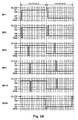
- FIG. 3A illustrates, in a first mode of operation of the display says normal, the shape of the line signals applied to the line electrodes of display.
- FIG. 3A only the line signals BP1, BP2, BP8 to BP10 and BP24 applied respectively to the electrodes of lines 101, 102, 108 to 110 and 124.
- Those skilled in the art will perfectly able to deduce the shape of the remaining line signals from the information that is given here.
- Each of the line signals BP1 to BP24 can take up to four levels separate voltage VLCD, V1, V4 and VSS.
- the VLCD and VSS voltages are activation levels and the voltages V1 and V4 of the non-activation levels.
- a pixel is not likely to be activated by a column signal suitable only if the corresponding line signal is simultaneously brought to the level activation voltage VLCD, respectively VSS.
- the non-activation voltages V1 and V4 are respectively defined at 83% and 17% of the activation voltage VLCD, VSS being chosen as a reference at 0 Volt.
- the signals of lines BP1 to BP24 thus vary between the activation voltage VSS and the voltage of no activation V1.
- the signals of line BP1 to BP24 vary between the activation voltage VLCD and the voltage of no activation V4.
- the line signal BP1 is briefly brought to the voltage VSS activation for a specific period T at the start of the first half-cycle A so activate line 101 of the display, then remains constant at the non-activation voltage V1 during the rest of half cycle A.
- the line signal BP1 is inverted compared to the previous half-cycle, i.e. the signal BP1 briefly switches to the activation voltage VLCD for a determined duration T at start of the next half-cycle B, then remains constant at the non-activation voltage V4 during the rest of half cycle B.
- line signal BP2 is briefly brought to the activation voltage VSS, respectively to the activation voltage VLCD, during the first half cycle A, respectively during the second half cycle B, just after passing the line signal BP1 to these same activation levels.
- the remaining line signals BP3 to BP24 are arranged analogously, the BP24 line signal being thus brought to the activation levels VSS, VLCD at the end of each half cycle A, B.
- each line signal BP1 to BP24 is brought sequentially once during a half-cycle A, B, for a determined duration T, at the activation voltage VSS, VLCD, so that the lines of the display are sequentially activated once during a half cycle period.
- the duration T during which the line signal is brought to the activation voltage is determined by the duration of each half cycle, i.e. by the frequency of display frames, as well as the number of display lines, here the number twenty-four. In the example illustrated, it will therefore be understood that each signal of line is brought to the activation voltage VSS, VLCD during 1 / 24th of the period of a half cycle. The rest of the time the line signal is brought to the no voltage activation V1, resp. V4.
- the lines are sequentially activated during each half-cycle, the activation and non-activation levels being alternated from one half cycle to another. At a given time, only one line of the display is not so activated, the other lines being all controlled by the non-activation voltage V1, V4.
- Adequate column signals are applied to the electrodes (not shown) of columns 201 to 205 of display 10 in order to selectively activate or turn off the display pixels.
- These line signals will be designated in the continuation of the description by the references FP1 to FP5, the signal FP1 corresponding to the column signal applied to the column electrode 201, the signal FP2 to the signal of column applied to the electrode of column 202 and so on until the signal FP5 applied to the column electrode 205.
- FIG. 3B illustrates, also in the first operating mode of the display, the shape of the column signals FP1 to FP5 applied to the electrodes of column (not shown) of the display 10 of FIG. 2. Also for the sake of simplification, in FIG. 3B, only the FP2 column signals have been shown and FP4 applied respectively to the electrodes of columns 202 and 204, that is to say the electrodes comprising in particular the pixels 11, 12 and 13 taken by way of example. Those skilled in the art will be perfectly able to deduce the appearance of the remaining column from Figure 2 and Figure 3B.
- the column signals FP1 to FP5 can also take up to four separate VLCD voltage levels, V2, V3 and VSS.
- the voltages V2 and V3 also constitute levels of no activation. It will be understood that a pixel is not likely to be activated by a signal of appropriate line only if the corresponding column signal is simultaneously fed at the activation voltage level VLCD or VSS, depending on the half-cycle considered.
- the non-activation voltages V2 and V3 are respectively defined at 66% and 34% of the activation voltage VLCD.
- the column signals FP1 to FP5 vary thus between the activation voltage VLCD and the non-activation voltage V2.
- the column signals FP1 to FP5 vary between the voltage VSS activation voltage and V3 non-activation voltage.
- the line signal FP2 illustrated in FIG. 3B is brought to time intervals determined during the first half cycle A, at the voltage activation button to activate the corresponding pixels in column 202 of the display, namely the pixels of lines 102 and 106 to 108.
- the column signal is brought to the non-activation level V2.
- the column signal FP2 is reversed with respect to in the previous half cycle, that is to say that the signal FP2 is brought to the voltage VSS activation at determined time intervals corresponding to the activation of pixels of lines 102 and 106 to 108, this signal FP2 being brought the rest of the time to level of non-activation V3.
- the column signal FP4 illustrated in FIG. 3B is brought, at time intervals determined during the first half-cycle A, to the activation voltage VLCD in order to activate the corresponding pixels in column 204 of the display, namely the pixels of lines 102 and 104, this FP4 signal remaining at level of non-activation V2 the rest of the time.
- the FP4 signal is reversed and is thus brought to the VSS activation level at intervals of time corresponding to the activation of the pixels of lines 102 and 104, this signal FP4 being brought the rest of the time to the level of non-activation V3.
- each column signal FP1 to FP5 is brought selectively, during a half-cycle A, B, at the activation voltage VLCD, VSS, in order activate the corresponding pixels in each of the columns 201 to 205 of display. It will therefore be understood that the signals making it possible to activate and deactivate the pixels in a column are multiplexed in time on each signal of column FP1 to FP5.
- the elementary duration during which the column signal is brought to the activation voltage VLCD, resp. VSS, to enable the activation of a determined pixel in the column corresponds to the duration T previously defined in relation to the line signals BP1 to BP24, i.e. 1 / 24th of the half-cycle period in this example.
- each half cycle A, B is broken down into this mode of operation in twenty-four sub-periods corresponding to twenty-four pixels that can be activated in each column of the display.
- multiplex rate means a parameter determined by the number of so-called active lines of the display and defining strictly speaking the number of active lines multiplexed on the signals of column FP1 to FP5.
- the twenty-four lines 101 to 124 of the display are active.
- T previously defined in relation to line signals BP1 to BP24, also the elementary duration during which the column signals are brought to the voltage activation to enable the activation of a determined pixel in the column, is directly related to this parameter.
- the multiplexing rate thus determines the shape of the line signals BP1 to BP24 as well as the intervals during which the column signals FP1 to FP5 must be brought to the activation level VLCD, resp. VSS, for selectively activate pixels.
- the multiplexing rate is reduced in proportion to the number of inactive lines.
- the rate of multiplexing will therefore be reduced to 1: 8 meaning that each half-cycle A, B is then broken down into eight sub-periods.
- FIGS. 4A to 4C will subsequently make it possible to highlight this point.
- FIG. 3C illustrates the signals at the terminals of pixels 11, 12, 13 resulting from the combination of the corresponding row and column signals.
- the three signals represented thus correspond respectively to the signal present at the boundaries of the pixel 11 resulting from the difference FP4-BP1 of the column signal FP4 and the line signal BP1, at the signal present at the terminals of pixel 12 resulting from the difference FP2-BP8 of column signal FP2 and line signal BP8 and to the signal present at the terminals of the pixel 13 resulting from the difference FP4-BP24 of the column signal FP4 and the signal of line BP24.
- the levels of tension activation VSS, VLCD and non-activation V1 to V4 are chosen so that the resulting signals at the terminals of the pixels present, over a period of two successive half-cycles, i.e. over a period encompassing half-cycles A and B in FIG. 3C, an average value substantially zero.
- the levels of non-activation V1 to V4 are chosen, in the example illustrated in Figures 3A to 3C, as fractions of the voltage VLCD activation (VSS being set as reference to 0 Volt) and so that the signal resulting at the terminals of each pixel is +/- V4 during twenty-three of the twenty-four sub-periods of each half-cycle, and +/- VLCD or +/- V2 during one of the twenty-four sub-periods depending on whether the pixel is active or inactive respectively.
- the non-activation voltages V1, V2 and V3 are worth VLCD-V4, VLCD-2V4 and 2V4 respectively.
- this signal is at + V2 during the first sub-period of the half cycle, then varies between +/- V4 during the twenty-three remaining sub-periods.
- the signal is inverted with respect to the preceding half-cycle A.
- this signal is at + VLCD, respectively -VLCD, during the eighth subperiod of the half cycle, and varies between +/- V4 during the other twenty-three sub-periods.
- a set of lines, called non-active, among the lines 101 to 124 of the display is disabled.
- Figures 4A to 4C illustrate only one choice from others. We could for example choose to keep active the first line 101 (such as a line of symbols) as well as the last seven lines 118 to 124 of display.
- FIGS. 4A to 4C for the sake of simplification, we have chosen to represent the signals with an identical number of activation levels and no activation. These activation and non-activating levels are also designated VSS, VLCD and V1, V2, V3, V4 respectively. Note however that the distribution of non-activation levels V1 to V4 is different, in this second mode of operation.
- the voltages of no activation V1 to V4 are respectively defined at 90%, 80%, 20% and 10% of the activation voltage VLCD. The reasons for this choice, which is by no means limiting, will be presented later. It will suffice for the moment to understand that this distribution non-activation voltages V1 to V4 is chosen in this way in order to compensate increasing the display contrast when switching from normal operation in standby mode.
- the signals applied to columns 201 to 205 of the display as well as the signals applied to the active lines 101 to 108 of the display are analogous to the signals applied during the first operating mode or normal mode.
- the rate of multiplexing is reduced in proportion to the number of disabled lines.
- the multiplexing rate is thus reduced to example of 1:24, in normal operating mode, to 1: 8 in standby operation. Consequently, the shape of the line signals BP1 to BP8 and column signals FP1 to FP5 is modified as illustrated in FIGS. 4A and 4B.
- Each half-cycle A, B of the line signals BP1 to BP8, respectively of the column signals FP1 to FP5 is thus broken down, in this second mode of operation, in eight sub-periods
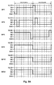
- FIG. 4A illustrates, in the second operating mode of the display, the shape of the line signals BP1 to BP24 applied to the line electrodes of display.
- line signals BP1, BP2, BP8 to BP10 and BP24 applied respectively on the electrodes of lines 101, 102, 108 to 110 and 124.
- the man of profession will be perfectly able to deduce the shape of the remaining line signals to from the information that is given here.
- the appearance of the line signals BP1 to BP8 applied, in the second mode of operation, on the active lines 101 to 108 of the display is analogous to the pace line signals BP1 to BP24 applied to lines 101 to 124 in the first operating mode.
- the multiplexing rate is reduced to 1: 8 in this second operating mode, it will be seen that the duration T during which each of the line signals BP1 to BP8 is brought to the level VSS activation, resp. VLCD is higher, in this second mode of operation, with respect to this same duration T, in the first mode of operation.
- the line signals BP1 to BP8 vary between the activation voltage VSS and the non-activation voltage V1.
- the line signals BP1 to BP8 vary between the activation voltage VLCD and the non-activation voltage V4.
- the line signal BP1 is briefly brought, at the start of each half-cycle A, B, at the activation voltage VSS, resp. VLCD, during 1 / 8th of the half-cycle period to activate line 101 of the display, then remain constant at the non-activation voltage V1, resp. V4 during the rest of the half cycle.
- line signal BP2 is briefly brought to the activation voltage VSS, resp. VLCD, during each half cycle A, B, just after passing the line signal BP1 to these same activation levels.
- Line signals BP3 to BP8 are arranged analogously, the line signal BP8 being thus brought to the levels of activation VSS, resp. VLCD, after each half cycle A, B, as illustrated in Figure 4A.
- each line signal BP1 to BP8 is brought sequentially once during a half cycle A, B, during 1 / 8th of the period of a half cycle, at activation voltage VSS, VLCD, so that the active lines 101 to 108 of the display are sequentially activated once during a half-cycle period.
- line activation signals are applied to the electrodes corresponding 109 to 124, so-called line activation signals. These signals are chosen so that when combined with the column signals FP1 to FP5, each pixel in these inactive lines 109 to 124 receives at its terminals a signal whose amplitude is too low to activate it.
- line non-activation signals which are supplied, for the duration of the first half-cycle A, at non-activation level V1, then, throughout the duration of the half-cycle according to B, at the non-activation level V4.
- FIG. 4B illustrates, also in the second operating mode of the display, the shape of the column signals FP1 to FP5 applied to the electrodes of column (not shown) of the display 10 of FIG. 2. Also for the sake of simplification, in FIG. 4B, only the FP2 column signals have been shown and FP4 applied respectively to the electrodes of columns 202 and 204, that is to say the electrodes comprising in particular the pixels 11, 12 and 13 taken by way of example. Those skilled in the art will be perfectly able to deduce the appearance of the remaining column from Figure 2 and Figure 4B.
- the appearance of column signals FP1 to FP5 applied, in the second operating mode, on columns 201 to 205 of the display is similar to the appearance of the signals applied to these same columns in the first operating mode.
- the multiplexing rate is reduced to 1: 8 in this second mode of operation, we can see that the time intervals during which the column signals FP1 to FP5 are brought to the activation levels VLCD, VSS so to activate the desired pixels are higher, in this second mode of operation, with respect to these same intervals, in the first mode of operation.
- this signal is at + V2 during the first sub-period of the half cycle, then varies between +/- V4 during the remaining seven sub-periods.
- the signal is inverted with respect to the preceding half-cycle A.
- V4 ⁇ VLCD
- ⁇ a parameter of distribution
- V ON, rms and V OFF, rms are directly dependent on the number of active lines of the display, ie on the multiplexing rate. It will also be noted that these values V ON, rms and V OFF, rms increase during a reduction in the multiplexing rate.
- this parameter ⁇ is approximately 17%.
- this parameter ⁇ is worth approximately 25%.
- FIGS. 5A to 5C illustrate, in the second mode of operation where the multiplex rate is 1: 8, other examples of line signals BP1 to BP24, column signals FP1 to FP5 and resulting signals present at the terminals of the pixels 11, 12, 13 in the case where the parameter ⁇ is chosen at 25% in order to optimize the display contrast for this multiplexing rate, only three levels of no activation is thus required in this case.
- VA 75% VLCD
- VB 50% VLCD
- VC 25% VLCD.
- the column signals such as the FP2 and FP4 signals illustrated in FIG. 4B, do not present only one level of VB non-activation in this case.
- a first variant it is thus possible to choose to optimize the contrast of the display for each operating mode and to choose accordingly the distribution (parameter ⁇ above) of the non-activation voltages.
- the contrast ratio V ON, rms / V OFF, rms
- This increase in contrast may be considered unpleasant for the user.
- the distribution of the voltages is adjusted not activating from one operating mode to another so as to maintain the substantially constant contrast.
- the non-activation voltages V1 to V4 are thus respectively defined at 90%, 80%, 20% and 10% of the activation voltage VLCD as shown in Figures 4A to 4C.
- the user can also decide not to adjust the contrast and tolerate a slight variation of the latter.
- the reduction in the multiplexing rate when switching from normal operating mode to standby operating mode is also accompanied by a reduction in the activation voltage VLCD (the activation voltage VSS is chosen as a reference to 0 Volts in both modes).
- the rms values or rms values V ON, rms and V OFF, rms increase when the multiplexing rate is reduced. It will thus be necessary to adjust the activation voltage VLCD so, for example, that the effective value V OFF, rms of the signal present at the terminals of a pixel in the non-active state is substantially constant from one operating mode to the other.
- the advantages of this invention are multiple.
- the reduction in the multiplexing rate and therefore of the frequency of multiplexing of the signals makes it possible to reduce the number of switching on the row and column electrodes of the display.
- the reduction in the multiplexing rate reduces the VLCD activation voltage of the pixels as already mentioned more high.
- the reduction in the multiplexing rate generates an increase in the display contrast which may or may not be adjustable by the user.
- the Applicant has observed that for a multiplexed display device with twenty-four lines active in normal operating mode and eight lines active in standby mode, reduced consumption at least two-thirds of energy was reached (the activation voltage VLCD being reduced when switching to standby mode).
- control method which has just been described can thus be applied from so as to switch a multiplexed display between a first mode of so-called normal operation (all lines active) and at least one second mode of standby operation (one or more inactive lines).
- This switching between modes can be done in software through a adequate programming of the control device or in hardware by the use of dedicated circuits. This switching can be automatic if desired.
- FIG. 6 We will now describe by means of FIG. 6, according to another aspect of the invention, an embodiment of a display control device multiplexed to implement the method described above.
- Figure 6 shows schematically a device or circuit control of a multiplexed display, generally designated by the reference digital device 30.
- This device 30 includes a mode switch 31, a programmable sequencer 32, a line signal generator 33, a means of shaping 34, a column signal generator 35, a voltage generator activation and non-activation 36 and a frequency generator 37.
- the mode switch 31 ensures, as its name suggests, a switching, automatic or manual, between normal operating mode and standby mode of operation. It controls the operation of the sequencer programmable 32, activation and non-activation voltage generator 36 as well frequency generator 37.
- the activation and non-activation voltage generator 36 is arranged to produce at its output the activation and non-activation voltages to be applied to the rows and columns of the display.
- this generator 36 produces at its output activation voltages VON, BP and non-activation voltages VOFF, BP for display lines. These voltages VON, BP and VOFF, BP are applied to line signal generator 33.
- the generator also produces at its output of the activation voltages VON, FP and of non activation VOFF, FP intended display columns. These voltages VON, FP and VOFF, FP are applied to the column signal generator 35.
- the voltages produced at the output of the activation voltage generator and non activation 36 are alternated from one half-cycle to the other as seen above.
- the generator 36 is therefore controlled by the programmable sequencer 32 of so as to ensure this alternation of activation and non-activation voltages.
- the generator 36 is controlled by the mode switch 31 so that that the activation and non-activation voltage levels are modified during the change from normal operating mode to standby operating mode.
- this generator 36 is arranged, on the one hand, to decrease the value of the activation voltage VLCD (VSS being chosen as reference at 0 Volt) in response to change from normal operating mode to standby operating mode, and to modify, on the other hand, the distribution of the non-activation voltages V1 to V4 in accordance with what has been described above.
- the activation voltage generator and non-activation 36 can decompose the activation voltage generator and non-activation 36 in a first block 361 controlled by the switch mode and used to generate activation voltages VSS, VLCD and no activation V1 to V4, and a second block 362 controlled by the sequencer programmable 32 so as to alternate activation and non-activation voltages from one half cycle to another.
- the frequency generator 37 includes an oscillator 371, a divider circuit 372 and a 373 frequency switch.
- Oscillator 371 and the circuit frequency divider 372 are arranged to produce a signal whose frequency determines the appearance of the row and column signals.
- the oscillator 371 and the frequency divider circuit 372 are arranged to deliver a first signal at a frequency f, called multiplexing, intended for the first mode of operation and a second signal at a frequency f / 3 intended for the second mode Operating.
- the frequency switch 373 controlled by the mode switch 31, delivers at its output a multiplexing signal of frequency f during the first mode and a multiplexing signal of frequency f / 3 during the second mode. This multiplexing signal is applied to the mode sequencer 32 and by means of shaping 34.
- the programmable sequencer 32 ensures the adequate sequence making it possible to generate the signals intended to be applied to the line electrodes of the display, such as the signals BP1 to BP24 presented previously.
- This sequencer programmable 32 is thus connected to line signal generator 33.
- the programmable sequencer 32 includes twenty-four outputs, connected to line signal generator 33, each of these outputs controlling the switching, in the line signal generator 33, between the activation voltages VON, BP and non-activation VOFF, BP according to the sequence described upper.
- the line signal generator 33 has twenty-four outputs, in this example, on which the line signals BP1 to BP24.
- the sequencer 32 In the normal operating mode, the sequencer 32 generates the adequate sequence for sequentially activating all lines of the display, i.e. the twenty-four lines of the display in this example.
- the generator 33 produces in response twenty-four line signals BP1 to BP24 such as signals illustrated in Figure 3A.
- the state of the outputs of the sequencer 32 in the normal operating mode over a period of half a cycle can for example be diagrammed, in the mode normal operation by a diagonal matrix, here a 24x24 matrix in which "1" and "0" correspond to the switching of the corresponding line signal respectively at the activation voltage and the non-activation voltage.
- the sequencer 32 produces the adequate sequence to activate the first eight lines of the display in this example.
- the last sixteen lines of the display are all kept at one not active state.
- the first eight outputs of the sequencer (from the left in figure 6) sequentially controls the switching of the eight first corresponding outputs of generator 33 between activation voltages and of non activation in order to produce the adequate signals BP1 to BP8 as illustrated in Figures 4A or 5A.
- the last sixteen outputs of sequencer 32 maintain the sixteen corresponding outputs of generator 33 at the non-activation voltage.
- the line signals BP9 to BP24 thus produced conform to the illustration of the figures 4A or 5A.
- the shaping means 34 ensures, as a function of the data to be displayed, the formatting of the column signals, in the example illustrated, the column signals FP1 to FP5. This shaping means 34 adequately controls the column signal generator 35.
- the line generator column signals 35 ensures adequate switching, for each column of the display of the column signals, here FP1 to FP5, between the activation voltages VON, FP and VOFF, FP non-activation produced by the voltage generator 36.
- the rate of multiplexing in normal operation is mainly determined by the number of lines of the display.
- the multiplexing rate in standby operating mode can perfectly be programmable so that it can be changed as desired by the user or display designer.
- the present invention can be adapted so that the display can occupy more than one operating mode of standby, for example a first standby operating mode in which the rate multiplexing is reduced by two, a second standby mode of operation in which the multiplexing rate is reduced by three, etc. Everything can perfectly be programmed.
- the present invention is therefore in no way limited to a display which can occupy only a normal operating mode and a single operating mode standby operation, but applies analogously if you want to plan more than one standby mode of operation.
- the method and the control device do not are not limited to the particular modes of implementation described in the present description.
- the method or the device applies well obviously similar to a display with a number of lines active different from twenty-four in normal operating mode and a number of active lines other than eight in standby mode.
- the figures illustrate only a few modes of implementation particular and not limiting of the present invention.
Landscapes
- Engineering & Computer Science (AREA)
- Chemical & Material Sciences (AREA)
- Crystallography & Structural Chemistry (AREA)
- Physics & Mathematics (AREA)
- Computer Hardware Design (AREA)
- General Physics & Mathematics (AREA)
- Theoretical Computer Science (AREA)
- Control Of Indicators Other Than Cathode Ray Tubes (AREA)
- Liquid Crystal Display Device Control (AREA)
Abstract
Description
- la figure 1, déjà présentée, montre un exemple conventionnel d'un dispositif d'affichage multiplexé;
- la figure 2 montre un exemple d'un dispositif d'affichage multiplexé comportant vingt-quatre lignes et cinq colonnes, utilisé dans le cadre d'un mode de mise en oeuvre particulier pour illustrer le principe de fonctionnement de la présente invention;
- les figures 3A et 3B illustrent, dans un premier mode de fonctionnement dit normal où les vingt-quatre lignes de l'affichage sont actives, des exemples de signaux pouvant être appliqués respectivement sur les lignes et sur les colonnes de l'affichage de la figure 2 pour sélectivement activer ou désactiver des pixels de cet affichage;
- la figure 3C illustre, dans le premier mode de fonctionnement, les signaux présents aux bornes de trois pixels de l'affichage de la figure 2, ces signaux résultant de la combinaison des signaux, illustrés aux figures 3A et 3B, appliqués sur les lignes et colonnes correspondantes de l'affichage;
- les figures 4A et 4B illustrent, dans un deuxième mode de fonctionnement dit de veille où seules les huit premières lignes de l'affichage sont actives, des exemples de signaux pouvant être appliqués respectivement sur les lignes et sur les colonnes de l'affichage de la figure 2 pour sélectivement activer ou désactiver des pixels de cet affichage;
- la figure 4C illustre, dans le deuxième mode de fonctionnement, les signaux présents aux bornes de trois pixels de l'affichage de la figure 2, ces signaux résultant de la combinaison des signaux, illustrés aux figures 4A et 4B, appliqués sur les lignes et colonnes correspondantes de l'affichage;
- les figures 5A et 5B illustrent, dans le deuxième mode de fonctionnement dit de veille où seules les huit premières lignes de l'affichage sont actives, d'autres exemples de signaux pouvant être appliqués respectivement sur les lignes et sur les colonnes de l'affichage de la figure 2 pour sélectivement activer ou désactiver des pixels de cet affichage;
- la figure 5C illustre, dans le deuxième mode de fonctionnement, les signaux présents aux bornes de trois pixels de l'affichage de la figure 2, ces signaux résultant de la combinaison des signaux, illustrés aux figures 5A et 5B, appliqués sur les lignes et colonnes correspondantes de l'affichage;
- la figure 6 montre schématiquement un exemple de réalisation d'un dispositif de commande d'un affichage multiplexé permettant de mettre en oeuvre le procédé de commande selon la présente invention.
Claims (10)
- Procédé de commande d'un affichage multiplexé (10) comportant une pluralité de pixels (11, 12, 13) agencés en lignes (101 à 124) et en colonnes (201 à 205) et couplés à des électrodes de ligne et à des électrodes de colonne, chacun desdits pixels (11, 12, 13) étant sélectivement activé ou désactivé par une combinaison déterminée d'un signal de ligne (BP1 à BP24) et d'un signal de colonne (FP1 à FP5) appliqués respectivement sur les électrodes de ligne et de colonne correspondantes, des lignes dites actives de l'affichage étant séquentiellement activées une fois au cours d'une période de un demi-cycle (A, B), procédé selon lequel ledit affichage est opéré dans un premier mode de fonctionnement dit normal dans lequel toutes les lignes de l'affichage sont activées, lesdits signaux de ligne et de colonne présentant un premier taux de multiplexage dit normal dans ledit premier mode de fonctionnement, procédé caractérisé en ce que :on commute ledit affichage dans au moins un deuxième mode de fonctionnement dit de veille, dans lequel des lignes dites non actives de l'affichage sont désactivées par l'application, sur les électrodes de lignes correspondantes, de signaux dits de non activation de ligne, ces signaux de non activation de ligne étant déterminés de telle sorte que, lorsqu'ils sont combinés avec les signaux de colonne (FP1 à FP5), chaque pixel desdites lignes non actives reçoit à ses bornes un signal dont l'amplitude est trop faible pour l'activer, eton agit, dans ledit au moins deuxième mode de fonctionnement, sur les signaux de ligne (BP1 à BP8) appliqués sur les lignes actives et sur lesdits signaux de colonne (FP1 à FP5) de manière à ce qu'ils présentent un second taux de multiplexage dont la valeur est réduite, par rapport au dit premier taux de multiplexage, en proportion du nombre de lignes non actives.
- Procédé selon la revendication 1, caractérisé en ce que :lesdites tensions d'activation (VLCD) et de non activation (V1 à V4; VA à VC) étant choisies de telle sorte que, sur une période de deux demi-cycles successifs, la valeur moyenne du signal présent aux bornes de chaque pixel est sensiblement nulle.lesdits signaux de ligne (BP1 à BP24; BP1 à BP8) varient, durant un premier demi-cycle (A), entre une tension de masse (VSS) et une première tension de non activation (V1; VA), et, durant un demi-cycle suivant (B), entre une tension d'activation (VLCD) et une deuxième tension de non activation (V4, VC),lesdits signaux de colonne (FP1 à FP5) varient, durant le premier demi-cycle (A), entre ladite tension d'activation (VLCD) et une troisième tension de non activation (V2; VB), et, durant le demi-cycle suivant (B), entre ladite tension de masse (VSS) et une quatrième tension de non activation (V3, VB),lesdits signaux de non activation de ligne sont amenés, durant toute la durée dudit premier demi-cycle (A), à ladite première tension de non-activation (V1; VA), et, durant toute la durée dudit demi-cycle suivant (B), à ladite deuxième tension de non activation (V4, VC),
- Procédé selon la revendication 2, caractérisé en ce que l'on diminue, lors du passage du premier au dit au moins deuxième mode de fonctionnement, la valeur de ladite tension d'activation (VLCD) de manière à compenser l'augmentation de la valeur efficace (VOFF,rms) du signal présent aux bornes d'un pixel non actif.
- Procédé selon la revendication 2 ou 3, caractérisé en ce que lesdites tensions de non activation (V1 à V4; VA à VC) sont déterminées, pour chaque mode de fonctionnement, de manière à maximiser le contraste de l'affichage.
- Procédé selon la revendication 2 ou 3, caractérisé en ce que lesdites tensions de non activation (V1 à V4, VA à VC) sont déterminées de telle sorte que le contraste de l'affichage reste sensiblement constant lors du passage du premier au dit au moins deuxième mode de fonctionnement.
- Dispositif de commande d'un affichage multiplexé (10) comportant une pluralité de pixels (11, 12, 13) agencés en lignes (101 à 124) et en colonnes (201 à 205) et couplés à des électrodes de ligne et à des électrodes de colonne, chacun desdits pixels (11, 12, 13) étant sélectivement activé ou désactivé par une combinaison déterminée d'un signal de ligne (BP1 à BP24) et d'un signal de colonne (FP1 à FP5) appliqués respectivement sur les électrodes de ligne et de colonne correspondantes, des lignes dites actives de l'affichage étant séquentiellement activées une fois au cours d'une période de un demi-cycle (A, B), ce dispositif étant susceptible de fonctionner dans un premier mode de fonctionnement dit normal dans lequel toutes les lignes de l'affichage sont activées, lesdits signaux de ligne et de colonne présentant un premier taux de multiplexage dit normal dans ledit premier mode de fonctionnement, ce dispositif de commande comprenant :caractérisé en ce que :des moyens générateur de fréquence (37) pour produire un signal de multiplexage ayant une fréquence f, dans ledit premier mode de fonctionnement, déterminant ledit premier taux de multiplexage;des moyens de production (32, 33) desdits signaux de ligne (BP1 à BP24) commandés par ledit signal de multiplexage;des moyens de production (34, 35) desdits signaux de colonne (FP1 à FP5) commandés par ledit signal de multiplexage; etdes moyens générateur de tensions (36) pour produire des tensions d'activation (VON,BP, VON,FP) et de non activation (VOFF,BP, VOFF,FP) destinées aux dits moyens de production (32, 33, 34, 35) des signaux de ligne et de colonne;le dispositif comprend en outre des moyens commutateur de mode (31) agencés pour commuter le dispositif entre ledit premier mode de fonctionnement et au moins un deuxième mode de fonctionnement dit de veille, dans lequel des lignes dites non actives de l'affichage sont désactivées, ces moyens commutateur de mode (31) commandant lesdits moyens (32, 33) de production des signaux de ligne ainsi que les moyens générateur de fréquence (37),lesdits moyens générateur de fréquence (37) sont agencés pour réduire la fréquence dudit signal de multiplexage en proportion du nombre de lignes non actives, en réponse au passage dans ledit au moins deuxième mode de fonctionnement, de telle sorte que les signaux de lignes (BP1 à BP8) appliqués sur les électrodes des lignes actives et lesdits signaux de colonne (FP1 à FP5) présentent un deuxième taux de multiplexage dont la valeur est réduite, par rapport au dit premier taux de multiplexage, en proportion du nombre de lignes non actives, etlesdits moyens de production (32, 34) des signaux de ligne sont agencés pour produire, dans ledit au moins deuxième mode de fonctionnement, des signaux dits de non activation de ligne sur les électrodes des lignes non actives, ces signaux de non activation de ligne étant déterminés de telle sorte que, lorsqu'ils sont combinés avec les signaux de colonne (FP1 à FP5), chaque pixel desdites lignes non actives reçoit à ses bornes un signal dont l'amplitude est trop faible pour l'activer.
- Dispositif selon la revendication 6, caractérisé en ce que lesdits moyens générateur de tensions (36) sont agencés pour produire une tension de masse (VSS), une tension d'activation (VLCD) et des première, deuxième, troisième et quatrième tensions de non activation (V1 à V4, VA à VC),lesdites tensions d'activation (VLCD) et de non activation (V1 à V4; VA à VC) étant choisies de telle sorte que, sur une période de deux demi-cycles successifs, la valeur moyenne du signal présent aux bornes de chaque pixel est sensiblement nulle.lesdits signaux de ligne (BP1 à BP24; BP1 à BP8) varient, durant un premier demi-cycle (A), entre ladite tension de masse (VSS) et ladite première tension de non activation (V1; VA), et, durant un demi-cycle suivant (B), entre ladite tension d'activation (VLCD) et ladite deuxième tension de non activation (V4, VC),lesdits signaux de colonne (FP1 à FP5) varient, durant le premier demi-cycle (A), entre ladite tension d'activation (VLCD) et ladite troisième tension de non activation (V2; VB), et, durant le demi-cycle suivant (B), entre ladite tension de masse (VSS) et ladite quatrième tension de non activation (V3, VB),lesdits signaux de non activation de ligne sont amenés, durant toute la durée dudit premier demi-cycle (A), à ladite première tension de non-activation (V1; VA), et, durant toute la durée dudit demi-cycle suivant (B), à ladite deuxième tension de non activation (V4, VC),
- Dispositif selon la revendication 7, caractérisé en ce que lesdits moyens commutateur de mode (31) commandent en outre lesdits moyens générateur de fréquence de telle sorte que la valeur de ladite tension d'activation (VLCD) est réduite, lors du passage du premier au dit au moins deuxième mode de fonctionnement, pour compenser l'augmentation de la valeur efficace (VOFF,rms) du signal présent aux bornes d'un pixel non actif.
- Dispositif selon la revendication 7 ou 8, caractérisé en ce que lesdites tensions de non activation (V1 à V4; VA à VC) sont déterminées, pour chaque mode de fonctionnement, de manière à maximiser le contraste de l'affichage.
- Dispositif selon la revendication 7 ou 8, caractérisé en ce que lesdites tensions de non activation (V1 à V4, VA à VC) sont déterminées de telle sorte que le contraste de l'affichage reste sensiblement constant lors du passage du premier au dit au moins deuxième mode de fonctionnement.
Priority Applications (6)
| Application Number | Priority Date | Filing Date | Title |
|---|---|---|---|
| EP00201217.7A EP1143405B1 (fr) | 2000-04-04 | 2000-04-04 | Procédé et dispositif de commande d'un affichage multiplexé avec mode de fonctionnement normal et mode de veille |
| PCT/CH2001/000159 WO2001075854A1 (fr) | 2000-04-04 | 2001-03-15 | Procede et dispositif de commande d'un affichage multiplexe avec mode de fonctionnement a consommation reduite |
| KR1020027013168A KR100773215B1 (ko) | 2000-04-04 | 2001-03-15 | 전력 소모 감소 모드에서 동작하는 멀티플렉싱된디스플레이 스크린의 제어 방법 및 장치 |
| CNB018102042A CN1244086C (zh) | 2000-04-04 | 2001-03-15 | 具有减低耗电工作模式的多路复用显示的控制方法和器件 |
| US10/239,413 US7180494B2 (en) | 2000-04-04 | 2001-03-15 | Method and device for controlling a multiplexed display screen operating in reduced consumption mode |
| JP2001573451A JP2003533711A (ja) | 2000-04-04 | 2001-03-15 | 多重化ディスプレイ用の制御方法およびデバイス |
Applications Claiming Priority (1)
| Application Number | Priority Date | Filing Date | Title |
|---|---|---|---|
| EP00201217.7A EP1143405B1 (fr) | 2000-04-04 | 2000-04-04 | Procédé et dispositif de commande d'un affichage multiplexé avec mode de fonctionnement normal et mode de veille |
Publications (2)
| Publication Number | Publication Date |
|---|---|
| EP1143405A1 true EP1143405A1 (fr) | 2001-10-10 |
| EP1143405B1 EP1143405B1 (fr) | 2016-06-01 |
Family
ID=8171305
Family Applications (1)
| Application Number | Title | Priority Date | Filing Date |
|---|---|---|---|
| EP00201217.7A Expired - Lifetime EP1143405B1 (fr) | 2000-04-04 | 2000-04-04 | Procédé et dispositif de commande d'un affichage multiplexé avec mode de fonctionnement normal et mode de veille |
Country Status (6)
| Country | Link |
|---|---|
| US (1) | US7180494B2 (fr) |
| EP (1) | EP1143405B1 (fr) |
| JP (1) | JP2003533711A (fr) |
| KR (1) | KR100773215B1 (fr) |
| CN (1) | CN1244086C (fr) |
| WO (1) | WO2001075854A1 (fr) |
Cited By (2)
| Publication number | Priority date | Publication date | Assignee | Title |
|---|---|---|---|---|
| GB2396697A (en) * | 2002-12-27 | 2004-06-30 | Schlumberger Holdings | Depth correction of drillstring measurements |
| US8181510B2 (en) | 2002-12-27 | 2012-05-22 | Schlumberger Technology Corporation | System and method for correcting errors in depth for measurements made while drilling |
Families Citing this family (8)
| Publication number | Priority date | Publication date | Assignee | Title |
|---|---|---|---|---|
| KR100496304B1 (ko) * | 2003-05-01 | 2005-06-17 | 삼성에스디아이 주식회사 | 효율적인 발진기들을 가진 디스플레이 패널의 구동 장치 |
| JP4151688B2 (ja) * | 2005-06-30 | 2008-09-17 | セイコーエプソン株式会社 | 集積回路装置及び電子機器 |
| KR100745982B1 (ko) * | 2006-06-19 | 2007-08-06 | 삼성전자주식회사 | 자발광형 디스플레이의 전력 저감을 위한 영상 처리 장치및 방법 |
| WO2009013824A1 (fr) * | 2007-07-25 | 2009-01-29 | Fujitsu Limited | Curseur de tête magnétique et dispositif à disque magnétique |
| US8121788B2 (en) * | 2007-12-21 | 2012-02-21 | Schlumberger Technology Corporation | Method and system to automatically correct LWD depth measurements |
| CN103137084B (zh) * | 2011-12-01 | 2015-02-25 | 微创高科有限公司 | 一种液晶显示器的驱动装置及驱动方法 |
| KR102071939B1 (ko) | 2013-05-23 | 2020-02-03 | 삼성디스플레이 주식회사 | 표시 장치 |
| KR102431311B1 (ko) * | 2015-01-15 | 2022-08-12 | 티씨엘 차이나 스타 옵토일렉트로닉스 테크놀로지 컴퍼니 리미티드 | 표시 장치 |
Citations (5)
| Publication number | Priority date | Publication date | Assignee | Title |
|---|---|---|---|---|
| US3976362A (en) * | 1973-10-19 | 1976-08-24 | Hitachi, Ltd. | Method of driving liquid crystal matrix display device |
| US5218352A (en) * | 1989-10-02 | 1993-06-08 | Matsushita Electric Industrial Co., Ltd. | Liquid crystal display circuit |
| EP0811866A1 (fr) * | 1995-12-14 | 1997-12-10 | Seiko Epson Corporation | Procede de pilotage d'afficheur, afficheur et appareil electronique |
| US5805121A (en) * | 1996-07-01 | 1998-09-08 | Motorola, Inc. | Liquid crystal display and turn-off method therefor |
| US5859625A (en) * | 1997-01-13 | 1999-01-12 | Motorola, Inc. | Display driver having a low power mode |
Family Cites Families (8)
| Publication number | Priority date | Publication date | Assignee | Title |
|---|---|---|---|---|
| JPS56116089A (en) * | 1980-02-19 | 1981-09-11 | Suwa Seikosha Kk | Liquid crystal display |
| US4910496A (en) * | 1987-01-08 | 1990-03-20 | Honda Giken Kogyo Kabushiki Kaisha | Direction indicating flasher device for vehicles with filament failure indication |
| JPH02131786U (fr) * | 1989-03-31 | 1990-11-01 | ||
| JPH07281632A (ja) * | 1994-04-04 | 1995-10-27 | Casio Comput Co Ltd | 液晶表示装置 |
| EP0721137B1 (fr) * | 1994-07-14 | 2004-01-21 | Seiko Epson Corporation | Circuit a sources de courant electrique, dispositif d'affichage a cristaux liquides et dispositif electronique |
| JPH10207438A (ja) * | 1996-11-21 | 1998-08-07 | Seiko Instr Inc | 液晶装置 |
| JP3572473B2 (ja) * | 1997-01-30 | 2004-10-06 | 株式会社ルネサステクノロジ | 液晶表示制御装置 |
| US6137466A (en) * | 1997-11-03 | 2000-10-24 | Motorola, Inc. | LCD driver module and method thereof |
-
2000
- 2000-04-04 EP EP00201217.7A patent/EP1143405B1/fr not_active Expired - Lifetime
-
2001
- 2001-03-15 JP JP2001573451A patent/JP2003533711A/ja active Pending
- 2001-03-15 KR KR1020027013168A patent/KR100773215B1/ko not_active Expired - Fee Related
- 2001-03-15 CN CNB018102042A patent/CN1244086C/zh not_active Expired - Fee Related
- 2001-03-15 US US10/239,413 patent/US7180494B2/en not_active Expired - Fee Related
- 2001-03-15 WO PCT/CH2001/000159 patent/WO2001075854A1/fr not_active Ceased
Patent Citations (5)
| Publication number | Priority date | Publication date | Assignee | Title |
|---|---|---|---|---|
| US3976362A (en) * | 1973-10-19 | 1976-08-24 | Hitachi, Ltd. | Method of driving liquid crystal matrix display device |
| US5218352A (en) * | 1989-10-02 | 1993-06-08 | Matsushita Electric Industrial Co., Ltd. | Liquid crystal display circuit |
| EP0811866A1 (fr) * | 1995-12-14 | 1997-12-10 | Seiko Epson Corporation | Procede de pilotage d'afficheur, afficheur et appareil electronique |
| US5805121A (en) * | 1996-07-01 | 1998-09-08 | Motorola, Inc. | Liquid crystal display and turn-off method therefor |
| US5859625A (en) * | 1997-01-13 | 1999-01-12 | Motorola, Inc. | Display driver having a low power mode |
Cited By (2)
| Publication number | Priority date | Publication date | Assignee | Title |
|---|---|---|---|---|
| GB2396697A (en) * | 2002-12-27 | 2004-06-30 | Schlumberger Holdings | Depth correction of drillstring measurements |
| US8181510B2 (en) | 2002-12-27 | 2012-05-22 | Schlumberger Technology Corporation | System and method for correcting errors in depth for measurements made while drilling |
Also Published As
| Publication number | Publication date |
|---|---|
| US7180494B2 (en) | 2007-02-20 |
| CN1436344A (zh) | 2003-08-13 |
| US20040090433A1 (en) | 2004-05-13 |
| JP2003533711A (ja) | 2003-11-11 |
| CN1244086C (zh) | 2006-03-01 |
| WO2001075854A1 (fr) | 2001-10-11 |
| KR20030024660A (ko) | 2003-03-26 |
| EP1143405B1 (fr) | 2016-06-01 |
| KR100773215B1 (ko) | 2007-11-02 |
Similar Documents
| Publication | Publication Date | Title |
|---|---|---|
| EP1143405B1 (fr) | Procédé et dispositif de commande d'un affichage multiplexé avec mode de fonctionnement normal et mode de veille | |
| EP0645888B1 (fr) | Ligne à retard numérique | |
| FR2707788A1 (fr) | Procédé et appareil pour réduire les discontinuités dans un système d'affichage à adressage actif. | |
| EP0655666A1 (fr) | Pièce d'horlogerie à affichage dynamique | |
| FR2530852A1 (fr) | Dispositif d'affichage d'images a cristal liquide | |
| FR2882881A1 (fr) | Procede et dispositifs de transmission d'informations tactiles | |
| EP1695332A2 (fr) | Cellule de commande electronique pour diode electroluminescente organique d afficheur a matrice active, procedes de fonctionn ement et afficheur | |
| EP0972282B1 (fr) | Dispositif de commande d'une cellule d'un ecran matriciel | |
| FR2648260A1 (fr) | Dispositif d'affichage a cristaux liquides | |
| CA3062288A1 (fr) | Procede et dispositif de generation de motifs tactiles | |
| FR2459505A1 (fr) | Montre electronique a sonneries multiples | |
| WO2004051357A1 (fr) | Dispositif d’affichage a cristal liquide nematique bistable et procede de commande d’un tel dispositif | |
| CH690404A5 (fr) | Récepteur de communication de données d'image | |
| EP1342132B1 (fr) | Procede d'entretien des oscillations d'un dispositif vibrant et dispositif vibrant mettant en oeuvre ce procede | |
| FR2492126A1 (fr) | Dispositif d'horlogerie analogique a affichage par cristaux liquides en multiplexage | |
| EP0907945B1 (fr) | Procede d'activation des cellules d'un ecran de visualisation d'image, et dispositif de visualisation d'image mettant en oeuvre le procede | |
| EP1875454B1 (fr) | Circuit et procede de commande d'affichage a segment a cristaux liquides | |
| EP2104092B1 (fr) | Dispositif d'affichage pouvant fonctionner en mode partiel d'affichage basse consommation | |
| EP3529796B1 (fr) | Procede de realisation d'un dispositif d'affichage bistable avec microcontroleur basse tension | |
| EP0798856B1 (fr) | Circuit de production d'impulsions avec répétition d'adresses | |
| FR3081241A1 (fr) | Procede de gestion de la valeur de la tension d'alimentation d'un module d'un circuit integre, et circuit integre associe | |
| BE1014890A4 (fr) | Circuit de traitement video. | |
| FR2646269A1 (fr) | Cellule d'affichage electro-optique perfectionnee | |
| WO2008101969A1 (fr) | Dispositif afficheur a cristal liquide comprenant des moyens perfectionnes de commutation | |
| EP1640943A2 (fr) | Procédé de commande d'un afficheur à cristaux liquides multi-segments |
Legal Events
| Date | Code | Title | Description |
|---|---|---|---|
| PUAI | Public reference made under article 153(3) epc to a published international application that has entered the european phase |
Free format text: ORIGINAL CODE: 0009012 |
|
| AK | Designated contracting states |
Kind code of ref document: A1 Designated state(s): AT BE CH CY DE DK ES FI FR GB GR IE IT LI LU MC NL PT SE |
|
| AX | Request for extension of the european patent |
Free format text: AL;LT;LV;MK;RO;SI |
|
| 17P | Request for examination filed |
Effective date: 20020410 |
|
| AKX | Designation fees paid |
Free format text: AT BE CH CY DE DK ES FI FR GB GR IE IT LI LU MC NL PT SE |
|
| 17Q | First examination report despatched |
Effective date: 20071109 |
|
| GRAP | Despatch of communication of intention to grant a patent |
Free format text: ORIGINAL CODE: EPIDOSNIGR1 |
|
| INTG | Intention to grant announced |
Effective date: 20160318 |
|
| GRAS | Grant fee paid |
Free format text: ORIGINAL CODE: EPIDOSNIGR3 |
|
| GRAA | (expected) grant |
Free format text: ORIGINAL CODE: 0009210 |
|
| AK | Designated contracting states |
Kind code of ref document: B1 Designated state(s): AT BE CH CY DE DK ES FI FR GB GR IE IT LI LU MC NL PT SE |
|
| REG | Reference to a national code |
Ref country code: GB Ref legal event code: FG4D Free format text: NOT ENGLISH |
|
| REG | Reference to a national code |
Ref country code: CH Ref legal event code: NV Representative=s name: ICB INGENIEURS CONSEILS EN BREVETS SA, CH Ref country code: CH Ref legal event code: EP Ref country code: AT Ref legal event code: REF Ref document number: 804297 Country of ref document: AT Kind code of ref document: T Effective date: 20160615 |
|
| REG | Reference to a national code |
Ref country code: IE Ref legal event code: FG4D Free format text: LANGUAGE OF EP DOCUMENT: FRENCH |
|
| REG | Reference to a national code |
Ref country code: DE Ref legal event code: R096 Ref document number: 60049343 Country of ref document: DE |
|
| REG | Reference to a national code |
Ref country code: NL Ref legal event code: MP Effective date: 20160601 |
|
| PG25 | Lapsed in a contracting state [announced via postgrant information from national office to epo] |
Ref country code: FI Free format text: LAPSE BECAUSE OF FAILURE TO SUBMIT A TRANSLATION OF THE DESCRIPTION OR TO PAY THE FEE WITHIN THE PRESCRIBED TIME-LIMIT Effective date: 20160601 |
|
| REG | Reference to a national code |
Ref country code: AT Ref legal event code: MK05 Ref document number: 804297 Country of ref document: AT Kind code of ref document: T Effective date: 20160601 |
|
| PG25 | Lapsed in a contracting state [announced via postgrant information from national office to epo] |
Ref country code: SE Free format text: LAPSE BECAUSE OF FAILURE TO SUBMIT A TRANSLATION OF THE DESCRIPTION OR TO PAY THE FEE WITHIN THE PRESCRIBED TIME-LIMIT Effective date: 20160601 Ref country code: GR Free format text: LAPSE BECAUSE OF FAILURE TO SUBMIT A TRANSLATION OF THE DESCRIPTION OR TO PAY THE FEE WITHIN THE PRESCRIBED TIME-LIMIT Effective date: 20160902 Ref country code: NL Free format text: LAPSE BECAUSE OF FAILURE TO SUBMIT A TRANSLATION OF THE DESCRIPTION OR TO PAY THE FEE WITHIN THE PRESCRIBED TIME-LIMIT Effective date: 20160601 Ref country code: ES Free format text: LAPSE BECAUSE OF FAILURE TO SUBMIT A TRANSLATION OF THE DESCRIPTION OR TO PAY THE FEE WITHIN THE PRESCRIBED TIME-LIMIT Effective date: 20160601 |
|
| PG25 | Lapsed in a contracting state [announced via postgrant information from national office to epo] |
Ref country code: IT Free format text: LAPSE BECAUSE OF FAILURE TO SUBMIT A TRANSLATION OF THE DESCRIPTION OR TO PAY THE FEE WITHIN THE PRESCRIBED TIME-LIMIT Effective date: 20160601 |
|
| PG25 | Lapsed in a contracting state [announced via postgrant information from national office to epo] |
Ref country code: PT Free format text: LAPSE BECAUSE OF FAILURE TO SUBMIT A TRANSLATION OF THE DESCRIPTION OR TO PAY THE FEE WITHIN THE PRESCRIBED TIME-LIMIT Effective date: 20161003 Ref country code: AT Free format text: LAPSE BECAUSE OF FAILURE TO SUBMIT A TRANSLATION OF THE DESCRIPTION OR TO PAY THE FEE WITHIN THE PRESCRIBED TIME-LIMIT Effective date: 20160601 |
|
| REG | Reference to a national code |
Ref country code: DE Ref legal event code: R097 Ref document number: 60049343 Country of ref document: DE |
|
| PLBE | No opposition filed within time limit |
Free format text: ORIGINAL CODE: 0009261 |
|
| STAA | Information on the status of an ep patent application or granted ep patent |
Free format text: STATUS: NO OPPOSITION FILED WITHIN TIME LIMIT |
|
| 26N | No opposition filed |
Effective date: 20170302 |
|
| PG25 | Lapsed in a contracting state [announced via postgrant information from national office to epo] |
Ref country code: DK Free format text: LAPSE BECAUSE OF FAILURE TO SUBMIT A TRANSLATION OF THE DESCRIPTION OR TO PAY THE FEE WITHIN THE PRESCRIBED TIME-LIMIT Effective date: 20160601 |
|
| REG | Reference to a national code |
Ref country code: DE Ref legal event code: R119 Ref document number: 60049343 Country of ref document: DE |
|
| REG | Reference to a national code |
Ref country code: CH Ref legal event code: PL |
|
| GBPC | Gb: european patent ceased through non-payment of renewal fee |
Effective date: 20170404 |
|
| REG | Reference to a national code |
Ref country code: IE Ref legal event code: MM4A |
|
| REG | Reference to a national code |
Ref country code: FR Ref legal event code: ST Effective date: 20171229 |
|
| PG25 | Lapsed in a contracting state [announced via postgrant information from national office to epo] |
Ref country code: MC Free format text: LAPSE BECAUSE OF FAILURE TO SUBMIT A TRANSLATION OF THE DESCRIPTION OR TO PAY THE FEE WITHIN THE PRESCRIBED TIME-LIMIT Effective date: 20160601 Ref country code: DE Free format text: LAPSE BECAUSE OF NON-PAYMENT OF DUE FEES Effective date: 20171103 Ref country code: FR Free format text: LAPSE BECAUSE OF NON-PAYMENT OF DUE FEES Effective date: 20170502 |
|
| PG25 | Lapsed in a contracting state [announced via postgrant information from national office to epo] |
Ref country code: CH Free format text: LAPSE BECAUSE OF NON-PAYMENT OF DUE FEES Effective date: 20170430 Ref country code: LU Free format text: LAPSE BECAUSE OF NON-PAYMENT OF DUE FEES Effective date: 20170404 Ref country code: GB Free format text: LAPSE BECAUSE OF NON-PAYMENT OF DUE FEES Effective date: 20170404 Ref country code: LI Free format text: LAPSE BECAUSE OF NON-PAYMENT OF DUE FEES Effective date: 20170430 |
|
| REG | Reference to a national code |
Ref country code: BE Ref legal event code: MM Effective date: 20170430 |
|
| PG25 | Lapsed in a contracting state [announced via postgrant information from national office to epo] |
Ref country code: IE Free format text: LAPSE BECAUSE OF NON-PAYMENT OF DUE FEES Effective date: 20170404 |
|
| PG25 | Lapsed in a contracting state [announced via postgrant information from national office to epo] |
Ref country code: BE Free format text: LAPSE BECAUSE OF NON-PAYMENT OF DUE FEES Effective date: 20170430 |
|
| PG25 | Lapsed in a contracting state [announced via postgrant information from national office to epo] |
Ref country code: CY Free format text: LAPSE BECAUSE OF NON-PAYMENT OF DUE FEES Effective date: 20160601 |