EP1143583A2 - Système de contact d'un barreau à laser à diode de haute puissance et méthode pour contacter un barreau à laser à diode de haute puissance - Google Patents
Système de contact d'un barreau à laser à diode de haute puissance et méthode pour contacter un barreau à laser à diode de haute puissance Download PDFInfo
- Publication number
- EP1143583A2 EP1143583A2 EP01107790A EP01107790A EP1143583A2 EP 1143583 A2 EP1143583 A2 EP 1143583A2 EP 01107790 A EP01107790 A EP 01107790A EP 01107790 A EP01107790 A EP 01107790A EP 1143583 A2 EP1143583 A2 EP 1143583A2
- Authority
- EP
- European Patent Office
- Prior art keywords
- hdb
- joining
- diode laser
- power diode
- adhesive
- Prior art date
- Legal status (The legal status is an assumption and is not a legal conclusion. Google has not performed a legal analysis and makes no representation as to the accuracy of the status listed.)
- Granted
Links
Images




Classifications
-
- H—ELECTRICITY
- H01—ELECTRIC ELEMENTS
- H01S—DEVICES USING THE PROCESS OF LIGHT AMPLIFICATION BY STIMULATED EMISSION OF RADIATION [LASER] TO AMPLIFY OR GENERATE LIGHT; DEVICES USING STIMULATED EMISSION OF ELECTROMAGNETIC RADIATION IN WAVE RANGES OTHER THAN OPTICAL
- H01S5/00—Semiconductor lasers
- H01S5/02—Structural details or components not essential to laser action
- H01S5/022—Mountings; Housings
- H01S5/0235—Method for mounting laser chips
- H01S5/02355—Fixing laser chips on mounts
- H01S5/0236—Fixing laser chips on mounts using an adhesive
-
- H—ELECTRICITY
- H01—ELECTRIC ELEMENTS
- H01S—DEVICES USING THE PROCESS OF LIGHT AMPLIFICATION BY STIMULATED EMISSION OF RADIATION [LASER] TO AMPLIFY OR GENERATE LIGHT; DEVICES USING STIMULATED EMISSION OF ELECTROMAGNETIC RADIATION IN WAVE RANGES OTHER THAN OPTICAL
- H01S5/00—Semiconductor lasers
- H01S5/02—Structural details or components not essential to laser action
- H01S5/022—Mountings; Housings
- H01S5/0233—Mounting configuration of laser chips
- H01S5/02345—Wire-bonding
-
- H—ELECTRICITY
- H01—ELECTRIC ELEMENTS
- H01S—DEVICES USING THE PROCESS OF LIGHT AMPLIFICATION BY STIMULATED EMISSION OF RADIATION [LASER] TO AMPLIFY OR GENERATE LIGHT; DEVICES USING STIMULATED EMISSION OF ELECTROMAGNETIC RADIATION IN WAVE RANGES OTHER THAN OPTICAL
- H01S5/00—Semiconductor lasers
- H01S5/02—Structural details or components not essential to laser action
- H01S5/022—Mountings; Housings
- H01S5/0235—Method for mounting laser chips
- H01S5/02355—Fixing laser chips on mounts
- H01S5/0237—Fixing laser chips on mounts by soldering
-
- H—ELECTRICITY
- H01—ELECTRIC ELEMENTS
- H01S—DEVICES USING THE PROCESS OF LIGHT AMPLIFICATION BY STIMULATED EMISSION OF RADIATION [LASER] TO AMPLIFY OR GENERATE LIGHT; DEVICES USING STIMULATED EMISSION OF ELECTROMAGNETIC RADIATION IN WAVE RANGES OTHER THAN OPTICAL
- H01S5/00—Semiconductor lasers
- H01S5/02—Structural details or components not essential to laser action
- H01S5/024—Arrangements for thermal management
- H01S5/02476—Heat spreaders, i.e. improving heat flow between laser chip and heat dissipating elements
-
- H—ELECTRICITY
- H01—ELECTRIC ELEMENTS
- H01S—DEVICES USING THE PROCESS OF LIGHT AMPLIFICATION BY STIMULATED EMISSION OF RADIATION [LASER] TO AMPLIFY OR GENERATE LIGHT; DEVICES USING STIMULATED EMISSION OF ELECTROMAGNETIC RADIATION IN WAVE RANGES OTHER THAN OPTICAL
- H01S5/00—Semiconductor lasers
- H01S5/40—Arrangement of two or more semiconductor lasers, not provided for in groups H01S5/02 - H01S5/30
- H01S5/4025—Array arrangements, e.g. constituted by discrete laser diodes or laser bar
- H01S5/4031—Edge-emitting structures
-
- H—ELECTRICITY
- H01—ELECTRIC ELEMENTS
- H01S—DEVICES USING THE PROCESS OF LIGHT AMPLIFICATION BY STIMULATED EMISSION OF RADIATION [LASER] TO AMPLIFY OR GENERATE LIGHT; DEVICES USING STIMULATED EMISSION OF ELECTROMAGNETIC RADIATION IN WAVE RANGES OTHER THAN OPTICAL
- H01S5/00—Semiconductor lasers
- H01S5/40—Arrangement of two or more semiconductor lasers, not provided for in groups H01S5/02 - H01S5/30
- H01S5/4025—Array arrangements, e.g. constituted by discrete laser diodes or laser bar
- H01S5/4031—Edge-emitting structures
- H01S5/4043—Edge-emitting structures with vertically stacked active layers
- H01S5/405—Two-dimensional arrays
-
- H—ELECTRICITY
- H10—SEMICONDUCTOR DEVICES; ELECTRIC SOLID-STATE DEVICES NOT OTHERWISE PROVIDED FOR
- H10W—GENERIC PACKAGES, INTERCONNECTIONS, CONNECTORS OR OTHER CONSTRUCTIONAL DETAILS OF DEVICES COVERED BY CLASS H10
- H10W72/00—Interconnections or connectors in packages
- H10W72/90—Bond pads, in general
-
- H—ELECTRICITY
- H10—SEMICONDUCTOR DEVICES; ELECTRIC SOLID-STATE DEVICES NOT OTHERWISE PROVIDED FOR
- H10W—GENERIC PACKAGES, INTERCONNECTIONS, CONNECTORS OR OTHER CONSTRUCTIONAL DETAILS OF DEVICES COVERED BY CLASS H10
- H10W72/00—Interconnections or connectors in packages
- H10W72/90—Bond pads, in general
- H10W72/941—Dispositions of bond pads
- H10W72/9415—Dispositions of bond pads relative to the surface, e.g. recessed, protruding
-
- H—ELECTRICITY
- H10—SEMICONDUCTOR DEVICES; ELECTRIC SOLID-STATE DEVICES NOT OTHERWISE PROVIDED FOR
- H10W—GENERIC PACKAGES, INTERCONNECTIONS, CONNECTORS OR OTHER CONSTRUCTIONAL DETAILS OF DEVICES COVERED BY CLASS H10
- H10W72/00—Interconnections or connectors in packages
- H10W72/90—Bond pads, in general
- H10W72/951—Materials of bond pads
- H10W72/952—Materials of bond pads comprising metals or metalloids, e.g. PbSn, Ag or Cu
-
- H—ELECTRICITY
- H10—SEMICONDUCTOR DEVICES; ELECTRIC SOLID-STATE DEVICES NOT OTHERWISE PROVIDED FOR
- H10W—GENERIC PACKAGES, INTERCONNECTIONS, CONNECTORS OR OTHER CONSTRUCTIONAL DETAILS OF DEVICES COVERED BY CLASS H10
- H10W90/00—Package configurations
- H10W90/701—Package configurations characterised by the relative positions of pads or connectors relative to package parts
- H10W90/721—Package configurations characterised by the relative positions of pads or connectors relative to package parts of bump connectors
- H10W90/724—Package configurations characterised by the relative positions of pads or connectors relative to package parts of bump connectors between a chip and a stacked insulating package substrate, interposer or RDL
Definitions
- High-power diode laser bars are semiconductor laser components of at least two optically essentially independently operable semiconductor laser emitters with a large optical output power. Their average optical line power densities exceed 1 watt / mm component width, their optical output powers exceed 10 watts cw per component.
- the reflection surfaces of the semiconductor laser resonators are called facets and can be mirrored or anti-reflective.
- HDB consist of a few 10 or 100 ⁇ m thick doped semiconductor substrate on which a pn junction has been epitaxially grown.
- HDB have two electrodes - an anode and a cathode which are on the substrate side and on the epitaxy side with respect to the HDB. A design of an electrode which is electrically isolated in terms of emitters on the epitaxy side enables individual operation of individual emitters.
- the electrodes of an HDB can be metallized or can also be unmetallized.
- HDB must be contacted for their operation.
- a contact with which an HBD connected can perform various functions. About these functions can count: the power supply to the HDB, the heat dissipation from the HDB and the mechanical fixation of the HDB.
- the contact can be particularly useful for HDB fulfill well if the connection between contact and HDB is cohesive.
- an ensemble is also made under an electrical contact for the HDB of several spatially spaced apart contact bodies of the same electrical polarity understood.
- an ensemble forms a series of electrical bond wires on the cathode of the HDB a single electrical
- N- forms a series of conductor tracks on one Ceramics used to contact the HDB on its anodes on the epitaxial side individual operation of the emitters is provided, a single electrical one (P-) contact.
- An electrical contact for an HDB can therefore consist of a variety of mechanical contacts exist.
- a high-power diode laser is understood to mean an HDB which is integrally connected with an electrically positive (p-) contact on the anode of the HDB and an electrically negative (n-) contact on the cathode of the HDB.
- the HDB of an HDL has exactly two electrical contacts - a positive and a negative - which are attached to the HDB on the epitaxial and substrate side.
- the HDB When operating the HDL, the HDB generates not only optical power but also one considerable part of thermal (power) loss, especially in the area of the pn-junction its emitter near the epitaxial side of the HDB.
- the electrical contacts of the HDB also take on a thermal function, by means of which thermal Performance of the HDB is dissipated. Have both electrical contacts of the HDL same thermal resistance, so more about the epitaxial contact thermal power (heat) dissipated than over the substrate side.
- an electrical Contact defined for the HDB via which more than a third of those in the HDB in Continuous wave (cw) operation generated thermal power can be dissipated.
- an HDB that is operated in the cw regime requires at least one electrical contact with a thermally relevant function.
- pulse regimes can operate both electrical contacts from subordinate thermal function, provided the time-averaged thermal Power two thirds of the value of the thermal peak power in the pulse is not exceeds.
- An example of an electrical contact with a thermally relevant function is a metallized diamond body onto which the HDB is soldered over a large area on the epitaxial side, and through which 90% of the heat produced in the HDB is dissipated during operation.
- An example of an electrical contact with a thermally subordinate function is a series of bonding wires that are connected to the electrode of the HDB was bonded and via which 1% of those produced in HDB in cw operation Heat is dissipated.
- Another example of electrical contact with thermally subordinate Function is a copper-tungsten substrate to which the HDB is soldered on the epitaxial side was and over that in pulse mode with a duty cycle of 35% in time Average 31.5% of the pulse peak heat output produced in the HDB or 90% of the HDB can be dissipated on average over the heat output produced.
- the integral connection of an HDB and an electrical contact includes a more or less pronounced joining zone between the two Link partners.
- the integral connection between an HDB and an electrical contact takes place in a material connection process, a joining process, after a joining process.
- the joining process can be done under the An additional joining material is involved.
- the joining process begins with the joining partners coming into contact with each other or with an additional joining material. It ends with reaching one cohesive connection, the properties of which the intended function of their Manufacturing fulfilled. These properties can include: sufficient electrical Conductivity, sufficient thermal conductivity, sufficient mechanical Strength.
- Arrangements of HDB and an electrical contact of a thermally subordinate function have a joining zone between the HDB and the electrical contact, which is designed as a bonded weld or solder joint.
- the joining zones differ depending on the joining process in that the joining zone between HDB and electrical contact is formed by an additional joining material, the solder, in the case of soldering, while the joining zone does not require any additional joining material during bonding.
- the electrical contact for example one or more Bond wires
- the electrical contact under the local influence of ultrasound, pressure and / or heat with connected to the HDB via its metallization.
- the local bond process Mechanical forces that occur can overload the HDB and to damage.
- the HDB must operate with a large number of Be bonded wires that can only be attached sequentially.
- adversely when contacting the HDB with bond wires is also that to compensate for the inhomogeneous power input to the HDB the latter with a particularly thick Metallization must be provided.
- wire bonding processes have one increased space requirements beyond the HDB. This is both disadvantageous for that Flexibility of the connection process as well as for the integration ability of HLD in Systems.
- connection is based on Diffusion processes between the solder material and the materials of the Metallization of the HDB and the electrical contact. The diffusion processes immediately begin contacting the metals and the solder Melting temperature of the solder or the metal-solder eutectic.
- a disadvantage of the soldering process is the required heat and its consequences:
- the Both joining partners, HDB and electrical contact usually have one different coefficients of thermal expansion.
- Voltage-reducing soft solders in turn tend to electromigration, which one sufficient HDB life are also detrimental.
- a major disadvantage is that all soldering processes use a flux or a forming gas as a reducing agent for the solder material need a reliable solder joint between the joining partners manufacture.
- these agents can damage sensitive facets of the HDB.
- a waiver of the joining process additional gaseous or liquid substances involved is therefore extreme desirable.
- the soldering process like the wire bonding process, requires one Metallization of the joining partners, especially the HDB. This represents the HDB production an additional complex process.
- the main advantage of a soldered connection is the good thermal Connection of a heat-generating joining partner to a heat-dissipating one Joining partner, is when connecting an HDB with an electrical contact from thermally subordinate function lapses.
- solder connections are as follows Dar: A solder joint always induces a harmful amount of mechanical Tensions in the HDB. If the mechanical stresses are low, there is for the connection the increased vulnerability to electromigration.
- Reducing agent for the solder material is at a low void and long-term stable Unavoidable soldering and is a danger to the facets.
- a disadvantage of the joining zones of cohesive HDB contact arrangements with one electrical contact of thermally subordinate function according to the state of the Technology is that the joining zones of the partners, HDB and contact, due to their The nature of the connection when damaging the HDB mechanical stresses or their facets of harmful chemical influences, exposes.
- the object of the invention is to provide a joining method for a cohesive connection of an HDB and an electrical contact of a thermally subordinate function, which does not have the disadvantages of conventional cohesive connections and the disadvantageous influences of conventional cohesive connection processes
- the object is achieved by means of a joining process which, with the participation of an adhesive HDB and electrical contact of a thermally subordinate function, connects to one another in an adhesion process.
- the object is achieved by an HDB contact arrangement with an electrical contact of a thermally subordinate function , the joining zone of which contains a joining material with an adhesive.
- an adhesive connection of Mais and HDB is the low mechanical stress of the joining zone: the beginning the adhesive bonding process takes place when the joining partners are brought into contact with the adhesive of the joining material.
- the joining process ends with the To achieve those properties of the joining zone that are necessary for the function of the Fulfill connection.
- the joining process can take place at room temperature and so that the laser is mechanically stress-free. He can Operating temperature of the laser and thus a mechanical for the laser enable voltage-free operation.
- the joining process can also be carried out at elevated temperature in order to achieve a Accelerating the joining process and / or an improvement in Achieve properties of the joining zone. It is assumed that the Adhesive-containing joining material due to plastic properties sufficient thickness of the joining zone with subsequent cooling developing thermomechanical tensions between the joining partners keeps a flow process low.
- the joining material is next to the adhesive contains electrically conductive material, for example a metallic filler, which improves the electrical connection between the contact and the HDB.
- the Joining material contains no other components apart from the adhesive. So very narrow joining zones can be achieved, even when using a non-metallic adhesive an electrically good conductive connection between the electrical contact and the HDB, for example if the thickness of the joining zone is in the area of the surface roughness of the joining partners.
- a preferred embodiment of the adhesive connection can be a solderable metallization of the HDB such as gold, and also the contact dispense because an adhesive does not necessarily need them. Even on one Diffusion barrier layer, as is customary for soldering, can, depending on the type of Adhesive and the fillers of the adhesive joining material, dispensed with become.
- a joining material with an adhesive can be relatively unproblematic with a Apply simple device directly to one of the joining partners without technically complex machines such as for solder vapor deposition or bonding therefor are necessary.
- the first exemplary embodiment shown in FIG. 1 shows an HDL (6) with an HDB (1), which consists of an approximately 100 ⁇ m thin n-doped GaAs substrate onto which a ternary or quaternary semiconductor heterostructure with the function of a pn- Transition to laser emitters (1a) with a final p-doped GaAs layer was applied epitaxially.
- the substrate (n-) side surface represents the cathode (1b) of the HDB, the epitaxial (p-) side surface the anode (1c).
- the cathode has a metallization (1d), the anode has a metallization (1e).
- the HDB (1) is soldered by means of a solder (5a) "p-side-down" over a solder joint (5) to a heat sink (4), which represents an electrical p-contact with a thermally relevant function.
- a metal film (2) made of copper approximately 50 ⁇ m thick represents the n-side electrical contact of thermally subordinate relevance to the HDB.
- the n-sided metallization of the HDB is considered to contain adhesive Joining material (3a) an electrically conductive adhesive (3b) applied.
- the thickness of the joining zone (3) adjusts to about 20 ⁇ m.
- the Joining process is continued by placing the elements at an elevated temperature of be stored at around 100 ° C.
- the adhesive (3b) is cured leads to the integral connection of the joining partners.
- a preferred variant of this first exemplary embodiment is based on the To dispense with metallizations (1d, 1e) of the HDB (1).
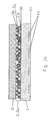
- Fig. 1a illustrates and consist in the metal film (2) openings (2b) or recesses (2c) in the form of grooves or pits, the can absorb excess joining material. So despite dosing inaccuracies achieve a sufficiently thin adhesive joint without the danger there is that the joining material swells in front of the facet of the HDB.
- Multiple openings (2b) side by side can equip the n-contact with contact lugs (2a) that also increase the flexibility of the metal film.
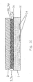
- FIG. 1b A preferred variant of the first exemplary embodiment is shown in FIG. 1b and consists in the use of a joining material (3a) in the joining zone (3) which in addition to the no longer necessarily electrically conductive adhesive (3b) a metallic filler of small silver particles from about 10 ⁇ m to a maximum Contains 20 ⁇ m size (3c). This addition lowers the electrical resistance of the Joining zone.
- the thickness of the joining zone is obtained by pressing the both joining surfaces of the contact partners, due to the largest silver particles in the Glue, to about 20 ⁇ m.
- FIG. 1c Another preferred variant of the first exemplary embodiment is in FIG. 1c shown and used with the same joining zone thickness instead of a silver particle (3c) a size of 10 ⁇ m to 20 ⁇ m only silver particles (3d) of less than 5 ⁇ m Size.
- a punctual increase in the contact pressure of Silver particles on the HDB can be avoided if the thickness of the joining zone (20 ⁇ m) is significantly larger than the particle size (5 ⁇ m).
- the second exemplary embodiment shown in FIG. 2 shows an HDL (6) with an HDB (1) addressable emitter (1a), which consists of an approximately 100 ⁇ m thin n-doped GaAs substrate onto which a ternary or quaternary semiconductor heterostructure is also present the function of a pn junction to laser emitters (1a) with a final p-doped GaAs layer was applied epitaxially.
- the substrate (n-) side surface represents the cathode (1b) of the HDB, the epitaxial (p-) side surface the anode (1c).
- the cathode carries a metallization (1d), the anode metallizations (1e) for each emitter.
- the HDB (1) is soldered on the substrate side by means of a solder (5a) "p-side-up" via a solder joint (5) to a heat sink (4), which represents an electrical n-contact with a thermally relevant function.
- An aluminum oxide ceramic substrate (2b) with conductor tracks made of thick-film gold (2a) of about 20 ⁇ m in height for each emitter represents the p-side electrical contact (2) of thermally subordinate relevance to the HDB (1).
- Both joining partners, HDB (1) and metallized ceramic (2), are made by Displacement of the joining material (3a) in contact with one another at room temperature brought by the conductor tracks (2a) the metallizations (1e) of the HDB (1) by their respective surface roughness.
- the thickness of the joining zone (3) lies in the order of magnitude between the two metallizations gamblenrauahtechnik. Between the conductor lines (between the emitters) lies the Thickness of the joining zone approximately at the thickness of the conductor tracks (20 ⁇ m).
- the curing of the Adhesive (3b) takes place at room temperature and leads to a material connection the joining partner. Even with curing at an elevated temperature would Cooling of the HDL (6) after the end of the joining process is hardly harmful Transfer voltages to the HDB because the aluminum oxide of the substrate has a coefficient of expansion similar to the GaAs.
- a preferred variant of this second embodiment can be a Improvement of the electrical transition in the joining zone between the conductor track (2a) and lead anode metallization (1e). It is illustrated in FIG. 2a and consists of the electrically insulating adhesive (3b) of the joining material (3a) a metallic filler of small silver particles (3c) of 10 ⁇ m in size to add fine distribution. This addition lowers the electrical resistance the joining zone (3) between conductor tracks (2a) and anode metallization (1e), if the thickness of the joining zone is adjusted to the size of the silver particles, and the Silver particles are brought into contact with both joining partners. Between The silver particles are so far apart from each other that there is no one between them significant electrical current can flow. The individual controllability of the emitter is guaranteed. This process of adhesive bonding becomes anisotropic called electrically conductive gluing.
- the third exemplary embodiment shown in FIG. 3 shows an HDL (6), which is intended for pulsed operation with 1 ms pulses at a 1 Hz repetition frequency, with two HDBs (1, 1 '), which are made from n-doped GaAs of approximately 100 ⁇ m -Substrate exist, on which ternary or quaternary semiconductor heterostructures with the function of pn junctions to laser emitters (1a, 1a ') was formed epitaxially with a final p-doped GaAs layer.
- the substrate (n-) side surface represents the cathode (1b, 1b ') of the HDB, the epitaxial (p-) side surface the anode (1c, 1c').
- the cathode has a metallization (1d, 1d '), the anode has a metallization (1e, 1e').
- a copper carrier (4) serves as an electrical p-contact from a thermally subordinate one Function for the first HDB (1) and is made with a layer of joining material (3a) provided, in addition to an adhesive (3b) electrically conductive particles (3c) made of gold contains less than 2 microns in size.
- the cathode metallizations (1d, 1d ') of the the first HDB (1) and the second HDB (1 ') are the same Joining material portions (3a ', 3a ").
- the first HDB (1) is inserted into the Layer of joining material (3a) of the copper carrier (4) pressed
- the second HDB (1 ') represents the n-contact of a thermally subordinate function for the first HDB (1) and is on the p-side in the layer joining material (3a ') on the cathode metallization (1d) of the first HDB (1) pressed.
- the first HDB (1) makes the p-contact of thermally subordinate function for the second HDB (1 ').
- a second Copper carrier (4 ') provides the n-contact of a thermally subordinate function the second HDB (1 ') and is in the layer joining material (3a ") on the Cathode metallization (1d ') of the second HDB (1') pressed.
- the curing of the Adhesive (3b) takes place at room temperature and leads to a material connection of all four joining partners In all cases there is a thickness of the three joining zones (3, 3 ', 3 ") from 2 to 4 ⁇ m.
- a preferred further development of the third exemplary embodiment consists in the Use of further, that is to say more than two, HDB in the HDB stack.
Landscapes
- Physics & Mathematics (AREA)
- Condensed Matter Physics & Semiconductors (AREA)
- General Physics & Mathematics (AREA)
- Electromagnetism (AREA)
- Optics & Photonics (AREA)
- Semiconductor Lasers (AREA)
- Wire Bonding (AREA)
- Cooling Or The Like Of Semiconductors Or Solid State Devices (AREA)
- Electric Connection Of Electric Components To Printed Circuits (AREA)
- Die Bonding (AREA)
- Adhesives Or Adhesive Processes (AREA)
Applications Claiming Priority (2)
| Application Number | Priority Date | Filing Date | Title |
|---|---|---|---|
| DE10018043 | 2000-04-07 | ||
| DE10018043A DE10018043A1 (de) | 2000-04-07 | 2000-04-07 | Verfahren zur Kontaktierung eines Hochleistungsdiodenlaserbarrens und eine Hochleistungsdiodenlaserbarren-Kontakt-Anordnung von elektrischen Kontakten thermisch untergeordneter Funktion |
Publications (3)
| Publication Number | Publication Date |
|---|---|
| EP1143583A2 true EP1143583A2 (fr) | 2001-10-10 |
| EP1143583A3 EP1143583A3 (fr) | 2003-12-17 |
| EP1143583B1 EP1143583B1 (fr) | 2005-10-19 |
Family
ID=7638413
Family Applications (1)
| Application Number | Title | Priority Date | Filing Date |
|---|---|---|---|
| EP01107790A Expired - Lifetime EP1143583B1 (fr) | 2000-04-07 | 2001-04-04 | Système de contact d'une barre de diodes laser haute puissance et méthode pour contacter cette barre de diodes laser haute puissance |
Country Status (5)
| Country | Link |
|---|---|
| US (1) | US6621839B1 (fr) |
| EP (1) | EP1143583B1 (fr) |
| JP (1) | JP2002009385A (fr) |
| AT (1) | ATE307406T1 (fr) |
| DE (2) | DE10018043A1 (fr) |
Cited By (1)
| Publication number | Priority date | Publication date | Assignee | Title |
|---|---|---|---|---|
| US11942763B2 (en) * | 2017-12-19 | 2024-03-26 | Osram Oled Gmbh | Semiconductor laser, operating method for a semiconductor laser, and method for determining the optimum fill factor of a semiconductor laser |
Families Citing this family (12)
| Publication number | Priority date | Publication date | Assignee | Title |
|---|---|---|---|---|
| JP4264231B2 (ja) | 2002-08-07 | 2009-05-13 | 浜松ホトニクス株式会社 | 集光装置 |
| JP4040934B2 (ja) | 2002-08-30 | 2008-01-30 | 浜松ホトニクス株式会社 | 集光装置 |
| JP4389696B2 (ja) * | 2004-07-02 | 2009-12-24 | ソニー株式会社 | 半導体装置およびその製造方法 |
| EP1811617A1 (fr) * | 2006-01-18 | 2007-07-25 | JENOPTIK Laserdiode GmbH | Base pour un arrangement vertical des barres de diode laser avec un arrêt |
| KR100764393B1 (ko) * | 2006-02-22 | 2007-10-05 | 삼성전기주식회사 | 고출력 어레이형 반도체 레이저 장치 제조방법 |
| JP4967851B2 (ja) * | 2007-06-26 | 2012-07-04 | セイコーエプソン株式会社 | 光源装置、プロジェクタ、モニタ装置 |
| DE102008026801B4 (de) * | 2008-06-02 | 2012-05-31 | Jenoptik Laser Gmbh | Wärmeübertragungsvorrichtung zur doppelseitigen Kühlung eines Halbleiterbauelementes und Verfahren zu seiner Montage |
| JP6806084B2 (ja) * | 2015-12-09 | 2021-01-06 | パナソニック株式会社 | 半導体発光装置 |
| CN106684707A (zh) * | 2017-03-13 | 2017-05-17 | 西安炬光科技股份有限公司 | 一种粘接型半导体激光器叠阵及其制备方法 |
| JP7152652B2 (ja) * | 2018-06-13 | 2022-10-13 | 日亜化学工業株式会社 | 光源装置 |
| DE102019124993A1 (de) * | 2019-09-16 | 2021-03-18 | Jenoptik Optical Systems Gmbh | Verfahren zum Herstellen einer Halbleiteranordnung und Diodenlaser |
| JPWO2023209939A1 (fr) * | 2022-04-28 | 2023-11-02 |
Family Cites Families (8)
| Publication number | Priority date | Publication date | Assignee | Title |
|---|---|---|---|---|
| US5284790A (en) * | 1990-01-03 | 1994-02-08 | Karpinski Arthur A | Method of fabricating monolithic laser diode array |
| US5212707A (en) * | 1991-12-06 | 1993-05-18 | Mcdonnell Douglas Corporation | Array of diffraction limited lasers and method of aligning same |
| US5325384A (en) * | 1992-01-09 | 1994-06-28 | Crystallume | Structure and method for mounting laser diode arrays |
| US6327285B1 (en) * | 1997-05-09 | 2001-12-04 | Semiconductor Laser International Corporation | Surface mounted 2-D diode laser array package |
| US6072814A (en) * | 1997-05-30 | 2000-06-06 | Videojet Systems International, Inc | Laser diode module with integral cooling |
| JPH11168263A (ja) * | 1997-09-30 | 1999-06-22 | Canon Inc | 光デバイス装置及びその製造方法 |
| US6295307B1 (en) * | 1997-10-14 | 2001-09-25 | Decade Products, Inc. | Laser diode assembly |
| US6259713B1 (en) * | 1997-12-15 | 2001-07-10 | The University Of Utah Research Foundation | Laser beam coupler, shaper and collimator device |
-
2000
- 2000-04-07 DE DE10018043A patent/DE10018043A1/de not_active Withdrawn
-
2001
- 2001-04-04 EP EP01107790A patent/EP1143583B1/fr not_active Expired - Lifetime
- 2001-04-04 DE DE50107728T patent/DE50107728D1/de not_active Expired - Lifetime
- 2001-04-04 JP JP2001106010A patent/JP2002009385A/ja active Pending
- 2001-04-04 AT AT01107790T patent/ATE307406T1/de not_active IP Right Cessation
- 2001-04-06 US US09/827,538 patent/US6621839B1/en not_active Expired - Lifetime
Cited By (1)
| Publication number | Priority date | Publication date | Assignee | Title |
|---|---|---|---|---|
| US11942763B2 (en) * | 2017-12-19 | 2024-03-26 | Osram Oled Gmbh | Semiconductor laser, operating method for a semiconductor laser, and method for determining the optimum fill factor of a semiconductor laser |
Also Published As
| Publication number | Publication date |
|---|---|
| DE10018043A1 (de) | 2001-10-11 |
| EP1143583B1 (fr) | 2005-10-19 |
| US6621839B1 (en) | 2003-09-16 |
| JP2002009385A (ja) | 2002-01-11 |
| ATE307406T1 (de) | 2005-11-15 |
| DE50107728D1 (de) | 2006-03-02 |
| EP1143583A3 (fr) | 2003-12-17 |
Similar Documents
| Publication | Publication Date | Title |
|---|---|---|
| EP0766354B1 (fr) | Elément de construction diode laser | |
| DE102011055891B4 (de) | Halbleiterlaserdiode | |
| DE69925524T2 (de) | Subträgerbaugruppe und damit verknüpfte Modulpackung | |
| EP1744415B1 (fr) | Boîtier pour dispositif à diode laser et dispositif à diode laser | |
| EP1143583B1 (fr) | Système de contact d'une barre de diodes laser haute puissance et méthode pour contacter cette barre de diodes laser haute puissance | |
| DE4338772A1 (de) | Diodenlaser-Stabanordnung | |
| DE112017000841T5 (de) | Halbleiterlaser-lichtquelleneinrichtung | |
| DE19536434C2 (de) | Verfahren zum Herstellen eines Halbleiterlaser-Bauelements | |
| DE112015004794T5 (de) | Laserlichtquellenvorrichtung | |
| DE102015013511B3 (de) | Laserstrahlungsquelle und Verfahren zur Herstellung einer Laserstrahlungsquelle und Verwendung eines Lötprozesses | |
| DE102012103160A1 (de) | Laserdiodenvorrichtung | |
| WO2021074050A2 (fr) | Socle d'un boîtier doté d'un composant électronique de transmission de signaux haute fréquence | |
| DE10361899A1 (de) | Diodenlasersubelement und Anordnungen mit derartigen Diodenlasersubelementen | |
| US20020172244A1 (en) | Self-separating laser diode assembly and method | |
| DE102008036439A1 (de) | Wärmeableitmodul mit einem Halbleiterelement und Herstellungsverfahren für ein solches Wärmeableitmodul | |
| WO2009079968A1 (fr) | Dispositif laser à semi-conducteur | |
| DE19644941C1 (de) | Hochleistungsdiodenlaser und Verfahren zu dessen Montage | |
| DE10040450B4 (de) | Halbleiterlaserbauelement mit einem Kühlelement | |
| DE4335512C2 (de) | Silizium-Mikrokanalkühler zur Kühlung von Hochleistungslaserdioden | |
| DE112020003541T5 (de) | Leistungshalbleitermodul | |
| DE102018121857B4 (de) | Vorrichtung zum Betreiben eines lichtemittierenden Halbleiterbauelements | |
| CN114204407B (zh) | 激光器管芯的封装结构及封装方法 | |
| WO2008031366A1 (fr) | Plaquette de circuits imprimés, en particulier plaquette en céramique | |
| WO2025051720A1 (fr) | Procédé de production d'un module de diode laser ainsi que substrat multicouche et composite laser à utiliser dans un procédé de production d'un module de diode laser | |
| DE112021002600B4 (de) | Verfahren zum herstellen einer halbleiterlaseranordnung und halbleiterlaseranordnung |
Legal Events
| Date | Code | Title | Description |
|---|---|---|---|
| PUAI | Public reference made under article 153(3) epc to a published international application that has entered the european phase |
Free format text: ORIGINAL CODE: 0009012 |
|
| AK | Designated contracting states |
Kind code of ref document: A2 Designated state(s): AT BE CH CY DE DK ES FI FR GB GR IE IT LI LU MC NL PT SE TR |
|
| AX | Request for extension of the european patent |
Free format text: AL;LT;LV;MK;RO;SI |
|
| PUAL | Search report despatched |
Free format text: ORIGINAL CODE: 0009013 |
|
| AK | Designated contracting states |
Kind code of ref document: A3 Designated state(s): AT BE CH CY DE DK ES FI FR GB GR IE IT LI LU MC NL PT SE TR |
|
| AX | Request for extension of the european patent |
Extension state: AL LT LV MK RO SI |
|
| 17P | Request for examination filed |
Effective date: 20040121 |
|
| 17Q | First examination report despatched |
Effective date: 20040405 |
|
| AKX | Designation fees paid |
Designated state(s): AT BE CH CY DE DK ES FI FR GB GR IE IT LI LU MC NL PT SE TR |
|
| GRAP | Despatch of communication of intention to grant a patent |
Free format text: ORIGINAL CODE: EPIDOSNIGR1 |
|
| GRAS | Grant fee paid |
Free format text: ORIGINAL CODE: EPIDOSNIGR3 |
|
| GRAA | (expected) grant |
Free format text: ORIGINAL CODE: 0009210 |
|
| AK | Designated contracting states |
Kind code of ref document: B1 Designated state(s): AT BE CH CY DE DK ES FI FR GB GR IE IT LI LU MC NL PT SE TR |
|
| PG25 | Lapsed in a contracting state [announced via postgrant information from national office to epo] |
Ref country code: IT Free format text: LAPSE BECAUSE OF FAILURE TO SUBMIT A TRANSLATION OF THE DESCRIPTION OR TO PAY THE FEE WITHIN THE PRESCRIBED TIME-LIMIT;WARNING: LAPSES OF ITALIAN PATENTS WITH EFFECTIVE DATE BEFORE 2007 MAY HAVE OCCURRED AT ANY TIME BEFORE 2007. THE CORRECT EFFECTIVE DATE MAY BE DIFFERENT FROM THE ONE RECORDED. Effective date: 20051019 Ref country code: FI Free format text: LAPSE BECAUSE OF FAILURE TO SUBMIT A TRANSLATION OF THE DESCRIPTION OR TO PAY THE FEE WITHIN THE PRESCRIBED TIME-LIMIT Effective date: 20051019 Ref country code: GB Free format text: LAPSE BECAUSE OF FAILURE TO SUBMIT A TRANSLATION OF THE DESCRIPTION OR TO PAY THE FEE WITHIN THE PRESCRIBED TIME-LIMIT Effective date: 20051019 Ref country code: IE Free format text: LAPSE BECAUSE OF FAILURE TO SUBMIT A TRANSLATION OF THE DESCRIPTION OR TO PAY THE FEE WITHIN THE PRESCRIBED TIME-LIMIT Effective date: 20051019 Ref country code: NL Free format text: LAPSE BECAUSE OF FAILURE TO SUBMIT A TRANSLATION OF THE DESCRIPTION OR TO PAY THE FEE WITHIN THE PRESCRIBED TIME-LIMIT Effective date: 20051019 |
|
| REG | Reference to a national code |
Ref country code: GB Ref legal event code: FG4D Free format text: NOT ENGLISH |
|
| REG | Reference to a national code |
Ref country code: CH Ref legal event code: EP |
|
| REG | Reference to a national code |
Ref country code: IE Ref legal event code: FG4D Free format text: LANGUAGE OF EP DOCUMENT: GERMAN |
|
| PG25 | Lapsed in a contracting state [announced via postgrant information from national office to epo] |
Ref country code: SE Free format text: LAPSE BECAUSE OF FAILURE TO SUBMIT A TRANSLATION OF THE DESCRIPTION OR TO PAY THE FEE WITHIN THE PRESCRIBED TIME-LIMIT Effective date: 20060119 Ref country code: GR Free format text: LAPSE BECAUSE OF FAILURE TO SUBMIT A TRANSLATION OF THE DESCRIPTION OR TO PAY THE FEE WITHIN THE PRESCRIBED TIME-LIMIT Effective date: 20060119 Ref country code: DK Free format text: LAPSE BECAUSE OF FAILURE TO SUBMIT A TRANSLATION OF THE DESCRIPTION OR TO PAY THE FEE WITHIN THE PRESCRIBED TIME-LIMIT Effective date: 20060119 |
|
| PG25 | Lapsed in a contracting state [announced via postgrant information from national office to epo] |
Ref country code: ES Free format text: LAPSE BECAUSE OF FAILURE TO SUBMIT A TRANSLATION OF THE DESCRIPTION OR TO PAY THE FEE WITHIN THE PRESCRIBED TIME-LIMIT Effective date: 20060130 |
|
| REF | Corresponds to: |
Ref document number: 50107728 Country of ref document: DE Date of ref document: 20060302 Kind code of ref document: P |
|
| PG25 | Lapsed in a contracting state [announced via postgrant information from national office to epo] |
Ref country code: PT Free format text: LAPSE BECAUSE OF FAILURE TO SUBMIT A TRANSLATION OF THE DESCRIPTION OR TO PAY THE FEE WITHIN THE PRESCRIBED TIME-LIMIT Effective date: 20060320 |
|
| NLV1 | Nl: lapsed or annulled due to failure to fulfill the requirements of art. 29p and 29m of the patents act | ||
| PG25 | Lapsed in a contracting state [announced via postgrant information from national office to epo] |
Ref country code: AT Free format text: LAPSE BECAUSE OF NON-PAYMENT OF DUE FEES Effective date: 20060404 |
|
| PG25 | Lapsed in a contracting state [announced via postgrant information from national office to epo] |
Ref country code: LI Free format text: LAPSE BECAUSE OF NON-PAYMENT OF DUE FEES Effective date: 20060430 Ref country code: MC Free format text: LAPSE BECAUSE OF NON-PAYMENT OF DUE FEES Effective date: 20060430 Ref country code: CH Free format text: LAPSE BECAUSE OF NON-PAYMENT OF DUE FEES Effective date: 20060430 Ref country code: BE Free format text: LAPSE BECAUSE OF NON-PAYMENT OF DUE FEES Effective date: 20060430 |
|
| GBV | Gb: ep patent (uk) treated as always having been void in accordance with gb section 77(7)/1977 [no translation filed] |
Effective date: 20051019 |
|
| REG | Reference to a national code |
Ref country code: IE Ref legal event code: FD4D |
|
| PLBE | No opposition filed within time limit |
Free format text: ORIGINAL CODE: 0009261 |
|
| STAA | Information on the status of an ep patent application or granted ep patent |
Free format text: STATUS: NO OPPOSITION FILED WITHIN TIME LIMIT |
|
| 26N | No opposition filed |
Effective date: 20060720 |
|
| EN | Fr: translation not filed | ||
| PG25 | Lapsed in a contracting state [announced via postgrant information from national office to epo] |
Ref country code: FR Free format text: LAPSE BECAUSE OF FAILURE TO SUBMIT A TRANSLATION OF THE DESCRIPTION OR TO PAY THE FEE WITHIN THE PRESCRIBED TIME-LIMIT Effective date: 20061208 |
|
| REG | Reference to a national code |
Ref country code: CH Ref legal event code: PL |
|
| BERE | Be: lapsed |
Owner name: JENOPTIK A.G. Effective date: 20060430 |
|
| PG25 | Lapsed in a contracting state [announced via postgrant information from national office to epo] |
Ref country code: LU Free format text: LAPSE BECAUSE OF NON-PAYMENT OF DUE FEES Effective date: 20060404 Ref country code: TR Free format text: LAPSE BECAUSE OF FAILURE TO SUBMIT A TRANSLATION OF THE DESCRIPTION OR TO PAY THE FEE WITHIN THE PRESCRIBED TIME-LIMIT Effective date: 20051019 |
|
| PG25 | Lapsed in a contracting state [announced via postgrant information from national office to epo] |
Ref country code: CY Free format text: LAPSE BECAUSE OF FAILURE TO SUBMIT A TRANSLATION OF THE DESCRIPTION OR TO PAY THE FEE WITHIN THE PRESCRIBED TIME-LIMIT Effective date: 20051019 Ref country code: FR Free format text: LAPSE BECAUSE OF FAILURE TO SUBMIT A TRANSLATION OF THE DESCRIPTION OR TO PAY THE FEE WITHIN THE PRESCRIBED TIME-LIMIT Effective date: 20051019 |
|
| REG | Reference to a national code |
Ref country code: DE Ref legal event code: R084 Ref document number: 50107728 Country of ref document: DE |
|
| REG | Reference to a national code |
Ref country code: DE Ref legal event code: R082 Ref document number: 50107728 Country of ref document: DE Representative=s name: WALDAUF, ALEXANDER, DIPL.-ING. DR.-ING., DE |
|
| REG | Reference to a national code |
Ref country code: DE Ref legal event code: R084 Ref document number: 50107728 Country of ref document: DE Effective date: 20150226 |
|
| REG | Reference to a national code |
Ref country code: DE Ref legal event code: R082 Ref document number: 50107728 Country of ref document: DE Representative=s name: WALDAUF, ALEXANDER, DIPL.-ING. DR.-ING., DE Ref country code: DE Ref legal event code: R081 Ref document number: 50107728 Country of ref document: DE Owner name: JENOPTIK OPTICAL SYSTEMS GMBH, DE Free format text: FORMER OWNER: JENOPTIK AG, 07743 JENA, DE |
|
| PGFP | Annual fee paid to national office [announced via postgrant information from national office to epo] |
Ref country code: DE Payment date: 20200423 Year of fee payment: 20 |
|
| REG | Reference to a national code |
Ref country code: DE Ref legal event code: R071 Ref document number: 50107728 Country of ref document: DE |