EP1146143A1 - Procédé et appareillage de nickelage et produit nickelé - Google Patents
Procédé et appareillage de nickelage et produit nickelé Download PDFInfo
- Publication number
- EP1146143A1 EP1146143A1 EP01302844A EP01302844A EP1146143A1 EP 1146143 A1 EP1146143 A1 EP 1146143A1 EP 01302844 A EP01302844 A EP 01302844A EP 01302844 A EP01302844 A EP 01302844A EP 1146143 A1 EP1146143 A1 EP 1146143A1
- Authority
- EP
- European Patent Office
- Prior art keywords
- layer
- plating
- substrate
- nickel
- drying
- Prior art date
- Legal status (The legal status is an assumption and is not a legal conclusion. Google has not performed a legal analysis and makes no representation as to the accuracy of the status listed.)
- Granted
Links
Images


Classifications
-
- C—CHEMISTRY; METALLURGY
- C23—COATING METALLIC MATERIAL; COATING MATERIAL WITH METALLIC MATERIAL; CHEMICAL SURFACE TREATMENT; DIFFUSION TREATMENT OF METALLIC MATERIAL; COATING BY VACUUM EVAPORATION, BY SPUTTERING, BY ION IMPLANTATION OR BY CHEMICAL VAPOUR DEPOSITION, IN GENERAL; INHIBITING CORROSION OF METALLIC MATERIAL OR INCRUSTATION IN GENERAL
- C23C—COATING METALLIC MATERIAL; COATING MATERIAL WITH METALLIC MATERIAL; SURFACE TREATMENT OF METALLIC MATERIAL BY DIFFUSION INTO THE SURFACE, BY CHEMICAL CONVERSION OR SUBSTITUTION; COATING BY VACUUM EVAPORATION, BY SPUTTERING, BY ION IMPLANTATION OR BY CHEMICAL VAPOUR DEPOSITION, IN GENERAL
- C23C18/00—Chemical coating by decomposition of either liquid compounds or solutions of the coating forming compounds, without leaving reaction products of surface material in the coating; Contact plating
- C23C18/16—Chemical coating by decomposition of either liquid compounds or solutions of the coating forming compounds, without leaving reaction products of surface material in the coating; Contact plating by reduction or substitution, e.g. electroless plating
- C23C18/31—Coating with metals
- C23C18/32—Coating with nickel, cobalt or mixtures thereof with phosphorus or boron
- C23C18/34—Coating with nickel, cobalt or mixtures thereof with phosphorus or boron using reducing agents
- C23C18/36—Coating with nickel, cobalt or mixtures thereof with phosphorus or boron using reducing agents using hypophosphites
-
- C—CHEMISTRY; METALLURGY
- C23—COATING METALLIC MATERIAL; COATING MATERIAL WITH METALLIC MATERIAL; CHEMICAL SURFACE TREATMENT; DIFFUSION TREATMENT OF METALLIC MATERIAL; COATING BY VACUUM EVAPORATION, BY SPUTTERING, BY ION IMPLANTATION OR BY CHEMICAL VAPOUR DEPOSITION, IN GENERAL; INHIBITING CORROSION OF METALLIC MATERIAL OR INCRUSTATION IN GENERAL
- C23C—COATING METALLIC MATERIAL; COATING MATERIAL WITH METALLIC MATERIAL; SURFACE TREATMENT OF METALLIC MATERIAL BY DIFFUSION INTO THE SURFACE, BY CHEMICAL CONVERSION OR SUBSTITUTION; COATING BY VACUUM EVAPORATION, BY SPUTTERING, BY ION IMPLANTATION OR BY CHEMICAL VAPOUR DEPOSITION, IN GENERAL
- C23C18/00—Chemical coating by decomposition of either liquid compounds or solutions of the coating forming compounds, without leaving reaction products of surface material in the coating; Contact plating
- C23C18/16—Chemical coating by decomposition of either liquid compounds or solutions of the coating forming compounds, without leaving reaction products of surface material in the coating; Contact plating by reduction or substitution, e.g. electroless plating
- C23C18/1601—Process or apparatus
- C23C18/1619—Apparatus for electroless plating
- C23C18/1628—Specific elements or parts of the apparatus
-
- C—CHEMISTRY; METALLURGY
- C23—COATING METALLIC MATERIAL; COATING MATERIAL WITH METALLIC MATERIAL; CHEMICAL SURFACE TREATMENT; DIFFUSION TREATMENT OF METALLIC MATERIAL; COATING BY VACUUM EVAPORATION, BY SPUTTERING, BY ION IMPLANTATION OR BY CHEMICAL VAPOUR DEPOSITION, IN GENERAL; INHIBITING CORROSION OF METALLIC MATERIAL OR INCRUSTATION IN GENERAL
- C23C—COATING METALLIC MATERIAL; COATING MATERIAL WITH METALLIC MATERIAL; SURFACE TREATMENT OF METALLIC MATERIAL BY DIFFUSION INTO THE SURFACE, BY CHEMICAL CONVERSION OR SUBSTITUTION; COATING BY VACUUM EVAPORATION, BY SPUTTERING, BY ION IMPLANTATION OR BY CHEMICAL VAPOUR DEPOSITION, IN GENERAL
- C23C18/00—Chemical coating by decomposition of either liquid compounds or solutions of the coating forming compounds, without leaving reaction products of surface material in the coating; Contact plating
- C23C18/16—Chemical coating by decomposition of either liquid compounds or solutions of the coating forming compounds, without leaving reaction products of surface material in the coating; Contact plating by reduction or substitution, e.g. electroless plating
- C23C18/1601—Process or apparatus
- C23C18/1633—Process of electroless plating
- C23C18/1646—Characteristics of the product obtained
- C23C18/165—Multilayered product
- C23C18/1651—Two or more layers only obtained by electroless plating
-
- C—CHEMISTRY; METALLURGY
- C23—COATING METALLIC MATERIAL; COATING MATERIAL WITH METALLIC MATERIAL; CHEMICAL SURFACE TREATMENT; DIFFUSION TREATMENT OF METALLIC MATERIAL; COATING BY VACUUM EVAPORATION, BY SPUTTERING, BY ION IMPLANTATION OR BY CHEMICAL VAPOUR DEPOSITION, IN GENERAL; INHIBITING CORROSION OF METALLIC MATERIAL OR INCRUSTATION IN GENERAL
- C23C—COATING METALLIC MATERIAL; COATING MATERIAL WITH METALLIC MATERIAL; SURFACE TREATMENT OF METALLIC MATERIAL BY DIFFUSION INTO THE SURFACE, BY CHEMICAL CONVERSION OR SUBSTITUTION; COATING BY VACUUM EVAPORATION, BY SPUTTERING, BY ION IMPLANTATION OR BY CHEMICAL VAPOUR DEPOSITION, IN GENERAL
- C23C18/00—Chemical coating by decomposition of either liquid compounds or solutions of the coating forming compounds, without leaving reaction products of surface material in the coating; Contact plating
- C23C18/16—Chemical coating by decomposition of either liquid compounds or solutions of the coating forming compounds, without leaving reaction products of surface material in the coating; Contact plating by reduction or substitution, e.g. electroless plating
- C23C18/1601—Process or apparatus
- C23C18/1633—Process of electroless plating
- C23C18/1675—Process conditions
- C23C18/1682—Control of atmosphere
-
- C—CHEMISTRY; METALLURGY
- C23—COATING METALLIC MATERIAL; COATING MATERIAL WITH METALLIC MATERIAL; CHEMICAL SURFACE TREATMENT; DIFFUSION TREATMENT OF METALLIC MATERIAL; COATING BY VACUUM EVAPORATION, BY SPUTTERING, BY ION IMPLANTATION OR BY CHEMICAL VAPOUR DEPOSITION, IN GENERAL; INHIBITING CORROSION OF METALLIC MATERIAL OR INCRUSTATION IN GENERAL
- C23C—COATING METALLIC MATERIAL; COATING MATERIAL WITH METALLIC MATERIAL; SURFACE TREATMENT OF METALLIC MATERIAL BY DIFFUSION INTO THE SURFACE, BY CHEMICAL CONVERSION OR SUBSTITUTION; COATING BY VACUUM EVAPORATION, BY SPUTTERING, BY ION IMPLANTATION OR BY CHEMICAL VAPOUR DEPOSITION, IN GENERAL
- C23C18/00—Chemical coating by decomposition of either liquid compounds or solutions of the coating forming compounds, without leaving reaction products of surface material in the coating; Contact plating
- C23C18/16—Chemical coating by decomposition of either liquid compounds or solutions of the coating forming compounds, without leaving reaction products of surface material in the coating; Contact plating by reduction or substitution, e.g. electroless plating
- C23C18/31—Coating with metals
- C23C18/32—Coating with nickel, cobalt or mixtures thereof with phosphorus or boron
- C23C18/34—Coating with nickel, cobalt or mixtures thereof with phosphorus or boron using reducing agents
-
- H—ELECTRICITY
- H05—ELECTRIC TECHNIQUES NOT OTHERWISE PROVIDED FOR
- H05K—PRINTED CIRCUITS; CASINGS OR CONSTRUCTIONAL DETAILS OF ELECTRIC APPARATUS; MANUFACTURE OF ASSEMBLAGES OF ELECTRICAL COMPONENTS
- H05K3/00—Apparatus or processes for manufacturing printed circuits
- H05K3/10—Apparatus or processes for manufacturing printed circuits in which conductive material is applied to the insulating support in such a manner as to form the desired conductive pattern
- H05K3/18—Apparatus or processes for manufacturing printed circuits in which conductive material is applied to the insulating support in such a manner as to form the desired conductive pattern using precipitation techniques to apply the conductive material
- H05K3/181—Apparatus or processes for manufacturing printed circuits in which conductive material is applied to the insulating support in such a manner as to form the desired conductive pattern using precipitation techniques to apply the conductive material by electroless plating
-
- C—CHEMISTRY; METALLURGY
- C23—COATING METALLIC MATERIAL; COATING MATERIAL WITH METALLIC MATERIAL; CHEMICAL SURFACE TREATMENT; DIFFUSION TREATMENT OF METALLIC MATERIAL; COATING BY VACUUM EVAPORATION, BY SPUTTERING, BY ION IMPLANTATION OR BY CHEMICAL VAPOUR DEPOSITION, IN GENERAL; INHIBITING CORROSION OF METALLIC MATERIAL OR INCRUSTATION IN GENERAL
- C23C—COATING METALLIC MATERIAL; COATING MATERIAL WITH METALLIC MATERIAL; SURFACE TREATMENT OF METALLIC MATERIAL BY DIFFUSION INTO THE SURFACE, BY CHEMICAL CONVERSION OR SUBSTITUTION; COATING BY VACUUM EVAPORATION, BY SPUTTERING, BY ION IMPLANTATION OR BY CHEMICAL VAPOUR DEPOSITION, IN GENERAL
- C23C18/00—Chemical coating by decomposition of either liquid compounds or solutions of the coating forming compounds, without leaving reaction products of surface material in the coating; Contact plating
- C23C18/16—Chemical coating by decomposition of either liquid compounds or solutions of the coating forming compounds, without leaving reaction products of surface material in the coating; Contact plating by reduction or substitution, e.g. electroless plating
- C23C18/18—Pretreatment of the material to be coated
- C23C18/1851—Pretreatment of the material to be coated of surfaces of non-metallic or semiconducting in organic material
- C23C18/1872—Pretreatment of the material to be coated of surfaces of non-metallic or semiconducting in organic material by chemical pretreatment
- C23C18/1886—Multistep pretreatment
- C23C18/1889—Multistep pretreatment with use of metal first
-
- Y—GENERAL TAGGING OF NEW TECHNOLOGICAL DEVELOPMENTS; GENERAL TAGGING OF CROSS-SECTIONAL TECHNOLOGIES SPANNING OVER SEVERAL SECTIONS OF THE IPC; TECHNICAL SUBJECTS COVERED BY FORMER USPC CROSS-REFERENCE ART COLLECTIONS [XRACs] AND DIGESTS
- Y10—TECHNICAL SUBJECTS COVERED BY FORMER USPC
- Y10T—TECHNICAL SUBJECTS COVERED BY FORMER US CLASSIFICATION
- Y10T428/00—Stock material or miscellaneous articles
- Y10T428/12—All metal or with adjacent metals
- Y10T428/12493—Composite; i.e., plural, adjacent, spatially distinct metal components [e.g., layers, joint, etc.]
- Y10T428/12771—Transition metal-base component
- Y10T428/12861—Group VIII or IB metal-base component
- Y10T428/12944—Ni-base component
Definitions
- the present invention relates to a process and an apparatus for nickel plating of an object such as electronic parts as well as a nickel-plated product produced by the apparatus according to the process.
- the present invention relates to a technique for electrolessly plating a Ni-B layer on the surface of a substrate and then a Ni-P layer thereon.
- a pattern is formed on a ceramic substrate which is then subjected to a pretreatment by sensitizing-activation process.
- a mask such as a resist may be stripped from the substrate which is then subjected to electroless Ni-P plating.
- the plating solution may comprises nickel salt (0.05-0.15mo/l), a complexing agent, tartrate or glycin (0.075-0.225mol/l), and a reducing agent, dimethylamine borane (0.5-4g/l).
- the Ni-B plating solution further contains sodium hydrate for adjusting the pH condition of the solution within the range of 5.0-7.0.
- the ceramic substrate is immersed the Ni-B plating solution which has been heated to 50°C for 20 minutes for plating.
- the Ni-P plating solution comprises nickel salt (0.05-0.15mo/l), a complexing agent, tartrate or glycin (0.075-0.225mol/l), and a reducing agent, sodium hypophosphite (10-30g/l).
- the Ni-P plating solution further contains sodium hydrate for adjusting the pH condition of the solution within the range of 5.0-7.0.
- the ceramic substrate is immersed in the Ni-P plating solution has been heated to 50°C for 50 minutes to obtain a nickel layer having a thickness of about 2 ⁇ m formed on the substrate.
- One object of the present invention is to provide a process for nickel plating which comprises the steps of electrolessly forming a Ni-B layer on a substrate and then a uniform and even Ni-P layer on the Ni-B layer.
- Another object of the present invention is to maintain the concentration of the Ni-B plating solution deposited on the substrate in the above-described process.
- One aspect of the present invention provides a nickel plating process which comprises the steps of: electrolessly plating a Ni-B layer on a substrate and then a Ni-P layer on the Ni-B plated substrate to obtain a substrate having a Ni-B layer formed on the surface thereof and a Ni-P layer superimposed on the Ni-B layer formed on the substrate.
- the substrate is subjected to drying-protection treatment after the Ni-B plating step and before the Ni-P plating step. In this way, a uniform and even Ni-P layer can be electrolessly plated on the electrolessly deposited Ni-B layer.
- a nickel plating apparatus which comprises: a Ni-B plating bath containing a Ni-B plating solution in which a substrate is immersed for electroless Ni-B deposition; a Ni-P plating bath containing a Ni-P plating solution in which the substrate having the Ni-B layer formed thereon is immersed for electroless Ni-P deposition; and a transporting member for transporting the substrate from the Ni-B plating bath to the Ni-P plating bath; wherein the Ni-B layer formed on the substrate is prevented from drying during the transportation of the substrate from the Ni-B plating bath to the Ni-P plating bath. In this way, a uniform and even Ni-P layer can be electrolessly plated on the electrolessly deposited Ni-B layer.
- the nickel placed product comprises: a surface; a Ni-B layer which is electrolessly plated on the surface; and a Ni-P layer having substantially uniform thickness which is electrolessly plated on the entire surface of the Ni-B layer. Accordingly, a nickel plated product which has a Ni-B layer and a substantially uniform Ni-P layer electrolessly formed thereon can be obtained by using the nickel plating apparatus and/or process of the present invention.
- One exemplary nickel plating process of the present invention will be described. Hereinafter, the process will be described for plating a nickel layer on a ceramic substrate (particularly a PZT substrate to be used for piezoelectric element).
- a dry film is pasted on a ceramic substrate which has been previously washed and degreased, and then exposed for development to form a pattern such that the dry film will remain on the surface of the ceramic substrate only in the areas which are not desirable to be plated.
- the ceramic substrate is placed in a solution of stannous fluoride (0.01-0.5 percent by weight) in aqueous hydrofluoric acid (0.001-0.1 percent by weight) for etching the surface of the ceramic substrate while depositing Sn ions thereon.
- the substrate is placed in a solution of palladium chloride (0.01-0.1 percent by weight) in aqueous hydrochloric acid (0.01-0.1 percent by weight) for substituting the Sn deposited on the surface of the substrate with palladium, thereby depositing palladium on the entire surface of the ceramic substrate.
- the dry film is stripped from the substrate by using aqueous sodium hydroxide.
- Ni-B and Ni-P plating solutions Two types of plating solutions (Ni-B and Ni-P plating solutions) are prepared.
- Ni-B plating solution comprises nickel salt (0.05-0.15mo/l), a complexing agent, tartrate or glycin (0.075-0.225mol/l), and a reducing agent, dimethylamine borane (0.5-4g/l). Ni-B plating solution also contains sodium hydrate for adjusting the pH condition of the solution within the range of 5.0-7.0.
- Ni-P plating solution comprises nickel salt (0.05-0.15mo/l), a complexing agent, tartrate or glycin (0.075-0.225mol/l), and a reducing agent, sodium hypophosphite (10-30g/l). Ni-P plating solution also contains sodium hydrate for adjusting the pH condition of the solution within the range of 5.0-7.0.
- the Ni-B plating solution prepared as described above is adjusted to pH6.5 at 50°C, and then used to plate the substrate for 20 minutes. Thus, Ni-B plating step is accomplished. After Ni-B plating step completed, the ceramic substrate is removed from the solution and immediately washed with water. When the ceramic substrate is plated in the solution at 50°C, for example, it may then be required to transport the substrate into the water in the washing bath from the solution within about 5 seconds.
- Ni-P plating step is accomplished to obtain a substrate having nickel lines of substantially uniform thickness formed thereon.
- Ni-B layer after Ni-B plating step and before the next electroless Ni-P plating step.
- a substrate was electrolessly plated with Ni-B layer, removed from the plating bath, and after 10 seconds, washed with water in a washing bath.
- a Ni-P layer was then formed on the substrate, which often resulted in an ununiform Ni-P layer.
- the present inventors found that it was difficult to form a uniform Ni-P layer on the electrolessly deposited Ni-B layer formed on the substrate if there was any dry area in the Ni-B layer where moisture is evaporated. This may be probably because a thin oxide film is formed on the surface of the Ni-B layer, which makes it difficult to deposit a Ni-P layer thereon.
- the ceramic substrate prior to the electroless Ni-P plating step, during transportation of a ceramic substrate from the plating bath to the washing bath after the substrate is electrolessly coated with a Ni-B layer, the ceramic substrate is subjected to a treatment for preventing the electrolessly plated Ni-B layer from drying.
- the drying-protection step is accomplished.
- the ambient atmosphere of the electrolessly plated Ni-B layer may be moistened to adjust the humidity.
- the electrolessly plated Ni-B layer may be contacted with any liquid by placing the substrate having the Ni-B layer formed thereon into the liquid or by applying or spraying the liquid onto the layer.
- Water may be used as the liquid though the Ni-B plating solution deposited onto the substrate may be disadvantageously diluted by the water. Therefore, Ni-B plating solution may be preferably used as the liquid.
- the evaporation of the moisture from the surface of Ni-B plating layer may be prevented by cooling the ceramic substrate to prevent it from drying.
- the surface of the ceramic substrate may partly become dry in several seconds after removed from the hot Ni-B plating solution though the time after removal from the plating solution and before start of the drying of the surface depends on the ambient temperature or humidity.
- the time after removal from the plating solution and before start of the drying of the surface depends on the ambient temperature or humidity.
- a nickel plating apparatus 1 as shown in Fig.s 1-4 can provide a solution to these problems by carrying out the above-described nickel-plating process.
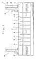
- Fig. 1 is a font view of the nickel plating apparatus 1 showing its general configuration.
- the nickel plating apparatus 1 comprises a liquid bath unit 2.
- the liquid bath unit 2 comprises a plurality of liquid bath sections: a loader stock 3 which contains hot pure water; Ni-B plating bath 4 which contains Ni-B electroless plating solution; washing baths 5, 6 and 7 which contain rinse water; Ni-P plating bath 8 which contains Ni-P electroless plating solution; washing baths 9, 10 and 11 which contain rinse water, and; an unloader stock 12 which contains pure water, which are serially arranged in the described order.
- the Ni-B plating bath 4 comprises a temperature controller for controlling the temperature of the Ni-B electroless plating solution contained therein, a vibrator for expelling bubble generated when the substrate is plated, a pH adjuster for controlling the pH range of the Ni-B electroless plating solution, an agitator for stirring the Ni-B electroless plating solution, and the like (not shown).
- Fresh water such as ion-exchange water is continuously supplied to the washing baths 5, 6, 7, 9, 10 and 11 by using, for example, running water.
- shower baths may also be used instead of running water baths.
- the liquid bath unit 2 is provided with a longitudinal guide-rail 13 parallel to the arrangement direction of the liquid baths 3-12. Caster wheels 14 are movable on the guide rail 13 in both the forward and reverse directions.
- each of the caster wheels 14 is provided a given elevating machine 15.
- the elevating machine 15 lifts and lowers a carrier 16.
- the carrier 16 is provided with a detachable holder plate 18 via a given supporting member 17.
- a ceramic substrate 19 to be plated can be mounted onto the holder 18.
- the elevating machine 15 can immerse the ceramic substrate 19 in a liquid contained in selected one of the liquid bath sections 3-12 by lowering the carrier 16 at the selected bath section while it can remove the ceramic substrate 19 from the one of the liquid bath sections 3-12 by lifting the carrier 16 from the section.
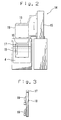
- the nickel plating apparatus 1 includes a controller 21 which comprises micon for collectively controlling many components.
- a controller 21 which comprises micon for collectively controlling many components.
- a motor 22 for driving the caster wheels 14 on the guide-rail 13
- a motor 23 for driving the elevating machine 15.
- a conductor tube 31 is connected to the Ni-B plating bath 4 for introducing Ni-Belectroless plating solution in the Ni-B plating bath 4 .
- the conductor tube 31 is provided with an electromagnetic valves 24-28, a pump 29 and a cooler 30.
- the conductor tube 31 is arranged such that the Ni-B electroless plating solution can be introduced through the tube into the following three pathways: a first pathway for sending the Ni-B electroless plating solution back to the Ni-B plating bath 4; a second pathway for spraying the Ni-B electroless plating solution via spray nozzles 32 provided on the inner surface of the Ni-B plating bath 4 and; a third pathway for draining the Ni-B electroless plating solution from the Ni-B plating bath 4.
- Various actuators and/or sensors are additionally connected to the controller 21, including the temperature controller, the vibrator, the pH adjuster and the agitator which are described above.
- Controller 21 drives the caster wheels 14 to place the ceramic substrate 19 to be plated above selected one of the liquid bath sections 3-12, and then drives the elevating machine 15 to lower the ceramic substrate 19 to place in the liquid in the selected bath section.
- the caster wheels 14 and the elevating machine 15 constitute a transporting mechanism.
- the ceramic substrate 19 which has been subjected to the above-described pretreatment step is then placed in a loader stock 3 .
- the substrate 19 is placed in the Ni-B electroless plating solution in the Ni-B plating bath 4 to electrolessly deposit Ni-B on the surface thereof, serially placed and washed with water in a series of the liquid bath sections 5-7, placed in the Ni-P electroless plating solution in the Ni-P plating bath 8 to electrolessly deposit Ni-P on the surface of the Ni-B layer, serially placed and washed with water in a series of the liquid bath sections 9-11, and then stored in the unloader stock 12.
- the time for immersion of the ceramic substrate 19 in the liquid contained in each of the liquid bath sections 3-12, and the temperature and pH conditions of the Ni-B plating bath 4 may be controlled by the controller 21.
- a controller 21 opens electromagnetic valves 24, 26 and 27 and drives a pump 29 and the cooler 30 to conduct the Ni-B electroless plating solution from the Ni-B plating bath 4 through the conductors 31, cool the solution with the cooler 30 and spray the solution via the spray nozzles 32.
- the electrolessly deposited Ni-P layer formed on the ceramic substrate 19 may be cooled down and moistened to prevent the surface thereof from drying.
- the drying-protection means and the liquid emitting device are implemented with the conductors 31, the electromagnetic valves 24, 26 and 27, the pump 29, the cooler 30, the spray nozzles 32 and the like.
- Ni-B electroless plating solution pure water may be sprayed on the ceramic substrate 19 to achieve the same effect.
- the Ni-B electroless plating solution may be preferably used since it can maintain the composition and the concentration of the Ni-B electroless plating solution deposited on the ceramic substrate 19.
- pure water or the like the amount of the Ni-B plating solution to be evaporated and the amount of the pure water or the like should be balanced.
- the Ni-B plating solution can be kept in a constant condition for use.
- the electromagnetic valve 28 is used for draining the Ni-B electroless plating solution from the Ni-B plating bath 4.
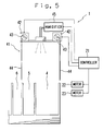
- This nickel plating apparatus 1 has the same configurations as those shown in Fig.s 1 to 3. The difference of this nickel plating apparatus 1 from the above-described nickel plating apparatus 1 is that it has the structure shown in Fig. 5 instead of that shown in Fig. 4. Hereinafter, this nickel plating apparatus 1 will be described with reference to Fig. 5, where the components identical to those of the above-described nickel plating apparatus 1 will be denoted by the same reference numerals and the detailed description thereof will be omitted.
- this nickel plating apparatus 1 is provided with a shutter unit 41 for covering the space above the Ni-B plating bath 4 and the washing bath 5, where transporting members such as a carrier 16 can pass through for transporting the ceramic substrate 19 from the Ni-B plating bath 4 to the washing bath 5.
- the shutter unit 41 is capable of driving winding devices 43, 43 via motors 42, 42 to open and close the shutters 44 and 44.
- the shutter unit 41 is also connected to a humidifier 45 (a drying-protection means ) to introduce steam into the space surrounded by the shutters 44, 44.
- the motors 42, 42 and the humidifier 45 are connected to a controller 21.
- the shutter unit 41 is illustrated to cover only the space above the Ni-B plating bath 4 and the washing bath 5, it may also cover all or part of the other liquid baths 6 to 12.
- the humidity inside the shutter unit 41 is regulated by the humidifier 45.
- the ceramic substrate 19 deposited with the Ni-B electroless plating solution is lifted to be positioned into the space inside the shutter unit 41 where humidity is at 80% or higher with respect to the saturated vapor pressure.
- evaporation rate of the moisture in the Ni-B layer deposited on the ceramic substrate 19 can be decreased.
- the surface(s) of the substrate(s) can be prevented from drying and thus a stable Ni-B/Ni-P laminated film can be formed.
- This nickel plating apparatus 1 is provided with a plurality of jigs 52 for holding the ceramic substrate 19 as shown in Fig. 6, which are mounted onto the holder 18.
- a Peltier element 51 that serves as a drying-protection means and as a cooler is provided on the backside surface of each of the jigs 52.
- the Peltier element 51 is connected to the controller 21.
- a predetermined heat sink is provided on the backside surface of the Peltier element 51, and the Peltier element 51 and the holder 18 are coated with Teflon.
- Other components of this nickel plating apparatus 1 are identical to those of the above-described nickel plating apparatuses 1 described with reference to Fig.s 1 to 4.
- structures identical to those of the above-described nickel plating apparatuses 1 will be denoted by the same reference numerals and the detailed description thereof will be omitted.
- the controller 21 turns on electricity to the Peltier element 51 to cool the jig 52 and thus the ceramic substrate 19 before plated. Then, the ceramic substrate 19 is lifted out from a Ni-B plating bath 4. By cooling the ceramic substrate 19 as described above, evaporation of the Ni-B layer is prevented, thereby preventing the surface of the ceramic substrate 19 from drying after the Ni-B deposition.
- a stable layered film can be formed by forming a Ni-B layer and then a Ni-P on the Ni-B layer while keeping the moisture on the surface of the Ni-B layer before the subsequent washing step thereby completely preventing the surface of the Ni-B layer from drying.
- Fig. 7 is a perspective view of the ceramic substrate 19 having nickel layer plated on the surface thereof which can be obtained according to any of the above-described production processes.
- Fig. 8 is a longitudinal cross-sectional view of the plate.
- lines 61 are formed by nickel deposition on the surface of the ceramic substrate 19 according to any of the above- described production processes. Specifically, the lines 61 are formed by electrolessly depositing a Ni-B layer 62 on the surface of the ceramic substrate 19, followed by electrolessly depositing a Ni-P layer 63 on the Ni-B layer 62. Since the lines 61 are formed by the above-described production process, there is no deterioration of the surface of the electrolessly deposited Ni-B layer 62, and thus the thickness of the electrolessly deposited Ni-P deposited layer 63 is substantially uniform across the entire surface.
- the surface of the electrolessly deposited Ni-B layer 62 can be prevented from deterioration, and the electrolessly deposited Ni-P layer 63 can thus be maintained substantially uniform such that the variation of the thickness of the layer 63 is within ⁇ 10 %.
- the variation of the thickness of an electrolessly deposited Ni-P layer 63 was as high as ⁇ 40 %.
- the present invention can provide a high-quality ceramic substrate 19 which has a substantially uniform electrolessly deposited Ni-P layer 63.
Landscapes
- Chemical & Material Sciences (AREA)
- Engineering & Computer Science (AREA)
- General Chemical & Material Sciences (AREA)
- Chemical Kinetics & Catalysis (AREA)
- Materials Engineering (AREA)
- Mechanical Engineering (AREA)
- Metallurgy (AREA)
- Organic Chemistry (AREA)
- Manufacturing & Machinery (AREA)
- Microelectronics & Electronic Packaging (AREA)
- Chemically Coating (AREA)
Applications Claiming Priority (4)
| Application Number | Priority Date | Filing Date | Title |
|---|---|---|---|
| JP2000108793 | 2000-04-11 | ||
| JP2000108793 | 2000-04-11 | ||
| JP2001060254 | 2001-03-05 | ||
| JP2001060254A JP2001355078A (ja) | 2000-04-11 | 2001-03-05 | ニッケルメッキ方法及びその装置並びに被メッキ物 |
Publications (2)
| Publication Number | Publication Date |
|---|---|
| EP1146143A1 true EP1146143A1 (fr) | 2001-10-17 |
| EP1146143B1 EP1146143B1 (fr) | 2005-12-07 |
Family
ID=26589824
Family Applications (1)
| Application Number | Title | Priority Date | Filing Date |
|---|---|---|---|
| EP01302844A Expired - Lifetime EP1146143B1 (fr) | 2000-04-11 | 2001-03-27 | Procédé et appareillage de nickelage |
Country Status (4)
| Country | Link |
|---|---|
| US (1) | US6555178B2 (fr) |
| EP (1) | EP1146143B1 (fr) |
| JP (1) | JP2001355078A (fr) |
| DE (1) | DE60115528T2 (fr) |
Cited By (1)
| Publication number | Priority date | Publication date | Assignee | Title |
|---|---|---|---|---|
| CN114672792A (zh) * | 2022-04-20 | 2022-06-28 | 深圳市恒博智造有限公司 | 一种具有负载及镀镍时间控制功能的镀镍用镍缸装置 |
Families Citing this family (5)
| Publication number | Priority date | Publication date | Assignee | Title |
|---|---|---|---|---|
| US6835667B2 (en) * | 2002-06-14 | 2004-12-28 | Fsi International, Inc. | Method for etching high-k films in solutions comprising dilute fluoride species |
| JP5211642B2 (ja) * | 2007-10-31 | 2013-06-12 | Jfeスチール株式会社 | 溶融亜鉛めっき鋼板の製造設備及び溶融亜鉛めっき鋼板の製造方法 |
| JP5581805B2 (ja) * | 2010-05-24 | 2014-09-03 | トヨタ自動車株式会社 | ステンレス鋼材へのめっき方法及びそのめっき材 |
| CN105586581B (zh) * | 2016-03-04 | 2017-12-12 | 济南大学 | 一种在水泥基压电复合材料表面化学镀镍的方法 |
| JPWO2017168745A1 (ja) * | 2016-04-01 | 2018-04-05 | 株式会社ケミトロン | 導体形成装置及び導体製造方法 |
Citations (4)
| Publication number | Priority date | Publication date | Assignee | Title |
|---|---|---|---|---|
| US4626479A (en) * | 1984-10-26 | 1986-12-02 | Kyocera Corporation | Covering metal structure for metallized metal layer in electronic part |
| EP0475567A2 (fr) * | 1990-09-12 | 1992-03-18 | Macdermid Incorporated | Méthode de fabrication de plaquettes à circuit imprimé |
| JPH06264284A (ja) * | 1993-03-15 | 1994-09-20 | Hitachi Ltd | 配線基板の形成方法 |
| EP0762814A1 (fr) * | 1995-08-22 | 1997-03-12 | Macdermid Incorporated | Procédé de fabrication de panneaux à circuit imprimé |
Family Cites Families (4)
| Publication number | Priority date | Publication date | Assignee | Title |
|---|---|---|---|---|
| US4745004A (en) * | 1987-01-08 | 1988-05-17 | Schwerin Thomas E | Method and apparatus for transporting circuit or other work units being processed |
| US4964365A (en) * | 1988-11-03 | 1990-10-23 | D.E.M. Controls Of Canada | Immersion process machine |
| JP3314125B2 (ja) | 1995-04-19 | 2002-08-12 | 東芝テック株式会社 | インクジェットプリンタヘッドの製造方法 |
| US5711806A (en) * | 1996-03-13 | 1998-01-27 | Harnden; Eric F. | Printed circuit board processing apparatus |
-
2001
- 2001-03-05 JP JP2001060254A patent/JP2001355078A/ja active Pending
- 2001-03-22 US US09/813,989 patent/US6555178B2/en not_active Expired - Fee Related
- 2001-03-27 EP EP01302844A patent/EP1146143B1/fr not_active Expired - Lifetime
- 2001-03-27 DE DE60115528T patent/DE60115528T2/de not_active Expired - Fee Related
Patent Citations (4)
| Publication number | Priority date | Publication date | Assignee | Title |
|---|---|---|---|---|
| US4626479A (en) * | 1984-10-26 | 1986-12-02 | Kyocera Corporation | Covering metal structure for metallized metal layer in electronic part |
| EP0475567A2 (fr) * | 1990-09-12 | 1992-03-18 | Macdermid Incorporated | Méthode de fabrication de plaquettes à circuit imprimé |
| JPH06264284A (ja) * | 1993-03-15 | 1994-09-20 | Hitachi Ltd | 配線基板の形成方法 |
| EP0762814A1 (fr) * | 1995-08-22 | 1997-03-12 | Macdermid Incorporated | Procédé de fabrication de panneaux à circuit imprimé |
Non-Patent Citations (1)
| Title |
|---|
| PATENT ABSTRACTS OF JAPAN vol. 018, no. 678 (C - 1290) 20 December 1994 (1994-12-20) * |
Cited By (1)
| Publication number | Priority date | Publication date | Assignee | Title |
|---|---|---|---|---|
| CN114672792A (zh) * | 2022-04-20 | 2022-06-28 | 深圳市恒博智造有限公司 | 一种具有负载及镀镍时间控制功能的镀镍用镍缸装置 |
Also Published As
| Publication number | Publication date |
|---|---|
| DE60115528D1 (de) | 2006-01-12 |
| JP2001355078A (ja) | 2001-12-25 |
| DE60115528T2 (de) | 2006-06-22 |
| US6555178B2 (en) | 2003-04-29 |
| US20010041267A1 (en) | 2001-11-15 |
| EP1146143B1 (fr) | 2005-12-07 |
Similar Documents
| Publication | Publication Date | Title |
|---|---|---|
| JP3960774B2 (ja) | 無電解めっき装置及び方法 | |
| JP4229954B2 (ja) | めっき処理ユニット | |
| US4659587A (en) | Electroless plating process and process for producing multilayer wiring board | |
| TWI385276B (zh) | 無電電鍍方法及設備 | |
| US7959977B2 (en) | Substrate processing method and apparatus | |
| KR101391533B1 (ko) | 무전해 도금 장치 및 무전해 도금 방법 | |
| GB2164063A (en) | Selective electroless deposition on insulating substrates | |
| JP2006507404A (ja) | 無電解メッキ槽の温度制御手順 | |
| JP2003129250A (ja) | めっき装置及びめっき方法 | |
| EP1146143B1 (fr) | Procédé et appareillage de nickelage | |
| JPWO2000074128A1 (ja) | 半導体装置の製造方法及び製造装置 | |
| US4066809A (en) | Method for preparing substrate surfaces for electroless deposition | |
| EP0007577A1 (fr) | Procédé pour améliorer l'adhésion des revêtements métalliques par voie chimique | |
| JP3998455B2 (ja) | 無電解めっき装置及び無電解めっき方法 | |
| US3839083A (en) | Selective metallization process | |
| JP4189876B2 (ja) | 基板処理装置 | |
| JP3712548B2 (ja) | 無電解銅めっき装置及び無電解銅めっき方法 | |
| JP4114456B2 (ja) | 無電解メッキ装置及び無電解メッキ方法 | |
| JP2002053972A (ja) | 無電解メッキ装置および無電解メッキ方法 | |
| US20050022909A1 (en) | Substrate processing method and substrate processing apparatus | |
| JP2005002443A (ja) | めっき方法及びめっき装置 | |
| JP3886383B2 (ja) | めっき装置及びめっき方法 | |
| JP2005060722A (ja) | 基板処理方法及び基板処理装置 | |
| EP3725912A1 (fr) | Agent de revêtement destiné à former un film d'oxyde, procédé destiné à produire un film d'oxyde et procédé destiné à produire une structure plaquée de métal | |
| CN121368403A (zh) | 封装基板的制造方法 |
Legal Events
| Date | Code | Title | Description |
|---|---|---|---|
| PUAI | Public reference made under article 153(3) epc to a published international application that has entered the european phase |
Free format text: ORIGINAL CODE: 0009012 |
|
| 17P | Request for examination filed |
Effective date: 20010405 |
|
| AK | Designated contracting states |
Kind code of ref document: A1 Designated state(s): AT BE CH CY DE DK ES FI FR GB GR IE IT LI LU MC NL PT SE TR Kind code of ref document: A1 Designated state(s): BE CH DE FR GB LI |
|
| AX | Request for extension of the european patent |
Free format text: AL;LT;LV;MK;RO;SI |
|
| AKX | Designation fees paid |
Free format text: BE CH DE FR GB LI |
|
| 17Q | First examination report despatched |
Effective date: 20030811 |
|
| GRAP | Despatch of communication of intention to grant a patent |
Free format text: ORIGINAL CODE: EPIDOSNIGR1 |
|
| RTI1 | Title (correction) |
Free format text: PROCESS AND APPARATUS FOR NICKEL PLATING |
|
| GRAS | Grant fee paid |
Free format text: ORIGINAL CODE: EPIDOSNIGR3 |
|
| GRAA | (expected) grant |
Free format text: ORIGINAL CODE: 0009210 |
|
| AK | Designated contracting states |
Kind code of ref document: B1 Designated state(s): BE CH DE FR GB LI |
|
| REG | Reference to a national code |
Ref country code: GB Ref legal event code: FG4D |
|
| REG | Reference to a national code |
Ref country code: CH Ref legal event code: EP |
|
| REF | Corresponds to: |
Ref document number: 60115528 Country of ref document: DE Date of ref document: 20060112 Kind code of ref document: P |
|
| REG | Reference to a national code |
Ref country code: CH Ref legal event code: NV Representative=s name: BOVARD AG PATENTANWAELTE |
|
| ET | Fr: translation filed | ||
| PLBE | No opposition filed within time limit |
Free format text: ORIGINAL CODE: 0009261 |
|
| STAA | Information on the status of an ep patent application or granted ep patent |
Free format text: STATUS: NO OPPOSITION FILED WITHIN TIME LIMIT |
|
| 26N | No opposition filed |
Effective date: 20060908 |
|
| PGFP | Annual fee paid to national office [announced via postgrant information from national office to epo] |
Ref country code: CH Payment date: 20080313 Year of fee payment: 8 |
|
| PGFP | Annual fee paid to national office [announced via postgrant information from national office to epo] |
Ref country code: FR Payment date: 20080311 Year of fee payment: 8 Ref country code: DE Payment date: 20080407 Year of fee payment: 8 |
|
| PGFP | Annual fee paid to national office [announced via postgrant information from national office to epo] |
Ref country code: BE Payment date: 20080522 Year of fee payment: 8 |
|
| PGFP | Annual fee paid to national office [announced via postgrant information from national office to epo] |
Ref country code: GB Payment date: 20080402 Year of fee payment: 8 |
|
| BERE | Be: lapsed |
Owner name: *TOSHIBA TEC K.K. Effective date: 20090331 |
|
| REG | Reference to a national code |
Ref country code: CH Ref legal event code: PL |
|
| GBPC | Gb: european patent ceased through non-payment of renewal fee |
Effective date: 20090327 |
|
| REG | Reference to a national code |
Ref country code: FR Ref legal event code: ST Effective date: 20091130 |
|
| PG25 | Lapsed in a contracting state [announced via postgrant information from national office to epo] |
Ref country code: LI Free format text: LAPSE BECAUSE OF NON-PAYMENT OF DUE FEES Effective date: 20090331 Ref country code: DE Free format text: LAPSE BECAUSE OF NON-PAYMENT OF DUE FEES Effective date: 20091001 Ref country code: CH Free format text: LAPSE BECAUSE OF NON-PAYMENT OF DUE FEES Effective date: 20090331 |
|
| PG25 | Lapsed in a contracting state [announced via postgrant information from national office to epo] |
Ref country code: BE Free format text: LAPSE BECAUSE OF NON-PAYMENT OF DUE FEES Effective date: 20090331 |
|
| PG25 | Lapsed in a contracting state [announced via postgrant information from national office to epo] |
Ref country code: GB Free format text: LAPSE BECAUSE OF NON-PAYMENT OF DUE FEES Effective date: 20090327 Ref country code: FR Free format text: LAPSE BECAUSE OF NON-PAYMENT OF DUE FEES Effective date: 20091123 |